 | –≠–ª–µ–∫—Ç—Ä–æ–Ω–Ω—ã–π –∫–æ–º–ø–æ–Ω–µ–Ω—Ç: CXD1910AQ | –°–∫–∞—á–∞—Ç—å:  PDF PDF  ZIP ZIP |
Description
The CXD1910AQ is a digital video encoder
designed for set top box, digital VCRs and other
digital video applications. The device accepts ITU-
R601 compatible Y, Cb, Cr data, and the data are
encoded to analog composite video and Y/C video
(S-Video) signal.
Features
∑ NTSC and PAL encoding mode
∑ Composite video and separate Y/C video (S-
Video) outputs
∑ Y, U, and V outputs
∑ 8/16-bit pixel data input mode
∑ 13.5 Mpps pixel rate
∑ 10-bit 3 channels DACs
∑ Supports I
2
C bus (400kHz) and SONY SIO
∑ Closed Caption (Line 21, Line 284) encoding
∑ Macrovision Pay-Per-View copy protection system
Rev. 6.1
∑ Monolithic CMOS single 5.0V power supply
∑ 64-pin plastic QFP package
This device is protected by U.S. patent numbers
4631603, 4577216 and 4819098 and other
intellectual property rights. Use of the Macrovision
anticopy process in the device is licensed by
Macrovision for non-commercial home use only.
Reverse engineering or disassembly is prohibited.
Absolute Maximum Ratings
∑ Supply voltage
V
DD
≠0.3 to +7.0
V
∑ Input voltage
V
I
≠0.3 to +7.0
V
∑ Output voltage
V
O
≠0.3 to +7.0
V
∑ Operating temperature Topr
≠20 to +75
∞C
∑ Storage temperature
Tstg
≠40 to +125
∞C
(Vss = 0V)
Recommended Operating Conditions
∑ Supply voltage
V
DD
4.75 to 5.25
V
∑ Input voltage
V
IN
Vss to V
DD
V
∑ Operating temperature Topr
0 to +70
∞C
I/O Capacitance
∑ Input pin
C
I
11 (Max.)
pF
∑ Output pin
C
O
11 (Max.)
pF
Note) Test conditions: V
DD
= V
I
= 0V
f
M
= 1MHz
≠ 1 ≠
CXD1910AQ
E95235A66-ST
Digital Video Encoder
Sony reserves the right to change products and specifications without prior notice. This information does not convey any license by
any implication or otherwise under any patents or other right. Application circuits shown, if any, are typical examples illustrating the
operation of the devices. Sony cannot assume responsibility for any problems arising out of the use of these circuits.
64 pin QFP (Plastic)
≠ 2 ≠
CXD1910AQ
X
R
S
T
P
D
0
t
o
7
P
D
8
t
o
1
5
P
D
C
L
K
S
Y
S
C
L
K
1
/
2
V
S
Y
N
C
H
S
Y
N
C
F
I
D
X
V
R
S
T
F
1
S
I
/
S
D
A
S
C
K
/
S
C
L
X
C
S
/
S
A
S
I
O
a
n
d
I
2
C
-
B
u
s
c
o
n
t
r
o
l
l
e
r
S
Y
N
C
g
e
n
.
a
n
d
t
i
m
i
n
g
c
o
n
t
r
o
l
l
e
r
D
e
m
p
x
,
l
e
v
e
l
t
r
a
n
s
l
a
t
o
r
a
n
d
i
n
t
e
r
p
o
l
a
t
o
r
4
:
2
:
2
t
o
4
:
4
:
4
U
V
D
e
l
a
y
L
P
F
L
P
F
M
o
d
u
l
a
t
o
r
C
H
R
O
M
A
B
U
R
S
T
F
L
A
G
C
S
Y
N
C
S
u
b
c
a
r
r
i
e
r
g
e
n
.
C
l
o
s
e
d
c
a
p
t
i
o
n
e
n
c
o
d
e
r
(
f
o
r
N
T
S
C
)
M
A
C
R
O
V
I
S
I
O
N
s
i
g
n
a
l
g
e
n
.
S
Y
N
C
s
l
o
p
e
g
e
n
.
Y
,
C
/
Y
,
U
,
V
s
e
l
e
c
t
o
r
a
n
d
i
n
t
e
r
p
o
l
a
t
o
r
1
0
b
i
t
D
A
C
1
0
b
i
t
D
A
C
1
0
b
i
t
D
A
C
V
B
Y
-
O
U
T
/
Y
C
O
M
P
-
O
/
V
C
-
O
U
T
/
U
V
G
I
R
E
F
V
R
E
F
T
D
O
T
D
I
T
M
S
T
C
K
T
R
S
T
5
7
5
9
6
0
6
2
5
1
5
2
4
8
4
9
5
0
5
6
2
5
2
9
2
4
3
2
2
6
2
0
2
1
4
6
4
3
4
4
4
5
4
1
1
t
o
4
,
6
t
o
9
1
1
t
o
1
8
Y
5
5
3
7
t
o
3
9
,
5
4
X
T
E
S
T
1
t
o
4
6
4
X
I
I
C
E
N
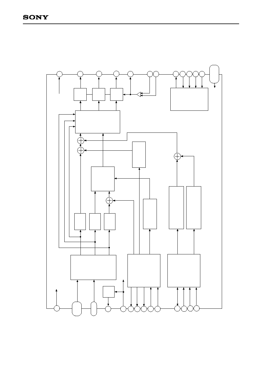
Block Diagram
≠ 3 ≠
CXD1910AQ
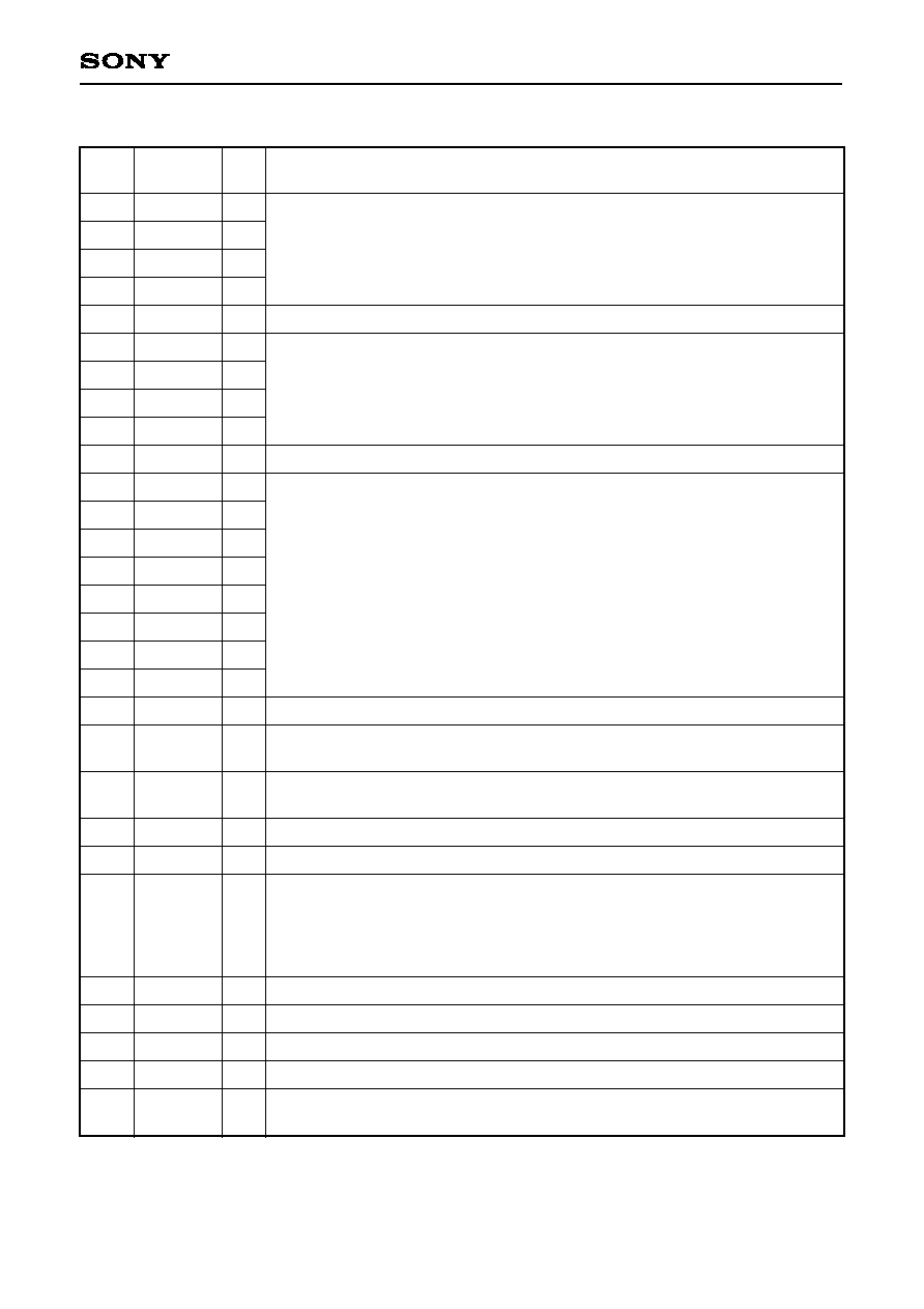
Pin Description
8-bit pixel data input pins (PD0 to 7).
When control register bit "PIF MODE" = "0":
These are inputs for multiplexed Y, Cb, and Cr signal.
When control register bit "PIF MODE" = "1":
These are inputs for Y signal.
Digital ground
8-bit pixel data input pins (PD0 to 7).
When control register bit "PIF MODE" = "0":
These are inputs for multiplexed Y, Cb, and Cr signal.
When control register bit "PIF MODE" = "1"
These are inputs for Y signal.
Digital power supply
Digital ground
The reference current output pin.
Connect resistance "16R" which is 16 times output resistance "R".
The voltage reference input pin.
Sets output full scale value.
Analog power supply
Analog ground
This is the output of 10-bit D/A converter.
When control register bit "YC/YUV" = "1":
This pin outputs composite signal.
When control register bit "YC/YUV" = "0":
This pin outputs color difference (V) signal.
Connect to V
SS
with a capacitor of approximately 0.1µF.
Connect to AV
DD
with a capacitor of approximately 0.1µF.
Analog power supply
Analog ground
This is the output of 10-bit D/A converter.
This pin outputs luminance (Y) signal.
8-bit pixel data input pins / Test data bus.
When control register bit "PIF MODE" = "0":
These inputs are not used.
When control register bit "PIF MODE" = "1":
These are inputs for multiplexed Cb and Cr signal.
When test mode, it's used for internal circuit test data bus.
Test mode is available only for device bender.
Pin
No.
1
2
3
4
5
6
7
8
9
10
11
12
13
14
15
16
17
18
19
20
21
22
23
24
25
26
27
28
29
PD7
PD6
PD5
PD4
V
SS
PD3
PD2
PD1
PD0
V
DD
PD15/TD7
PD14/TD6
PD13/TD5
PD12/TD4
PD11/TD3
PD10/TD2
PD9/TD1
PD8/TD0
V
SS
IREF
VREF
AV
DD
1
AV
SS
1
COMP-O/V
VB
VG
AV
DD
2
AV
SS
2
Y-OUT/Y
I
I
I
I
--
I
I
I
I
--
I/O
I/O
I/O
I/O
I/O
I/O
I/O
I/O
--
O
I
--
--
O
O
I
--
--
O
Symbol
I/O
Description
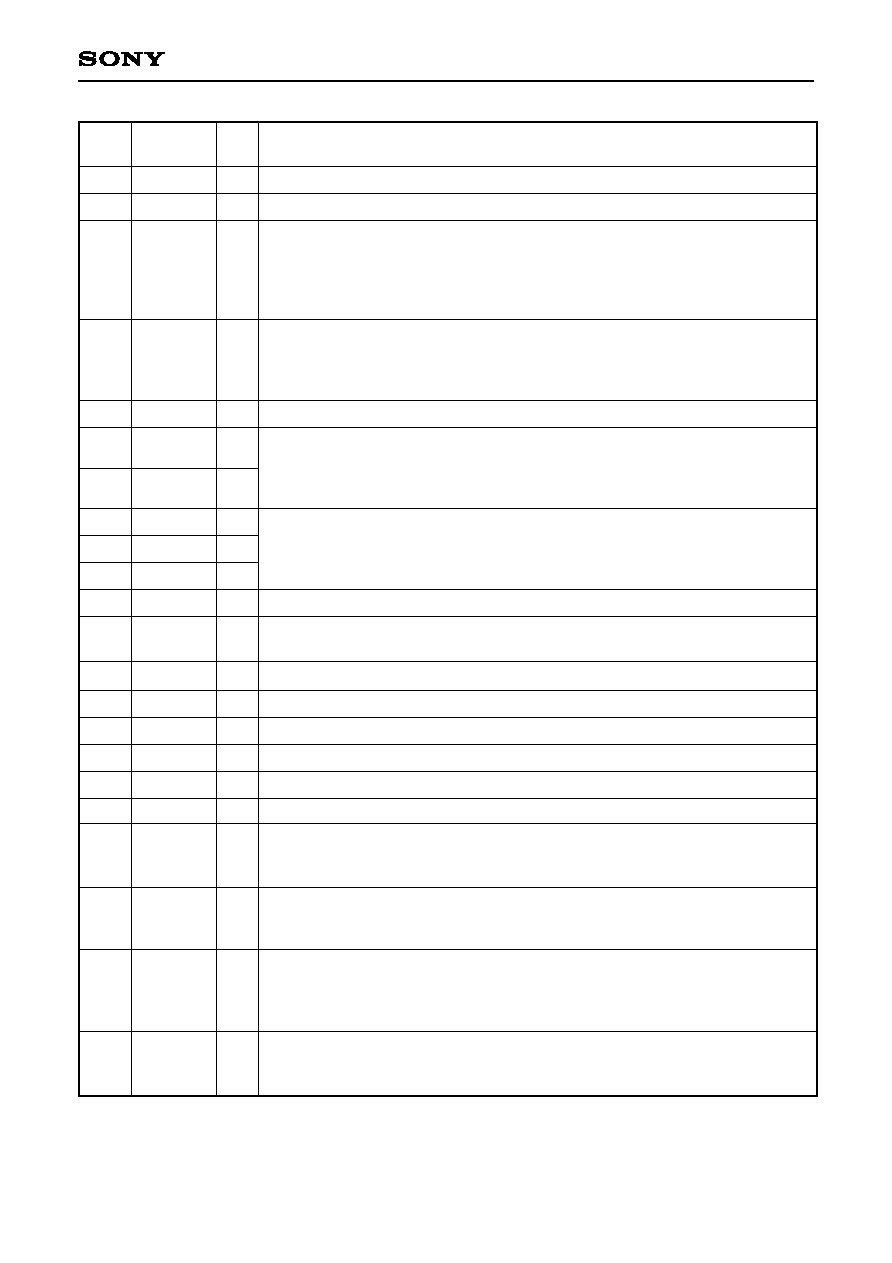
≠ 4 ≠
CXD1910AQ
Analog power supply
Analog ground
This is the output of 10-bit D/A converter.
When control register bit "YC/YUV" = "1":
This pin outputs chroma (C) signal.
When control register bit "YC/YUV" = "0":
This pin outputs color difference (U) signal.
Test data bus.
This pin should be open.
When test mode, it's used for internal circuit test data bus.
Test mode is available only for device bender.
Digital power supply
Test data bus.
These pins should be open.
When test mode, it's used for internal circuit test data bus.
Test mode is available only for device bender.
Test mode control input pins. These pins are pulled up.
When these pins are "H", the CXD1910AQ is not test mode.
Test mode is available only for device bender.
Digital ground
Test mode reset input pins.
When power on reset, set "L" for more than 40 clocks (SYSCLK).
Digital power supply
Test mode control input pins. This pin is pulled up.
Test mode control input pins. This pin is pulled up.
Test mode control input pins. This pin should be "H" input.
Test data bus. This pin should be open.
Digital ground
This pin's function is selected by XIICEN (Pin 64).
When XIICEN = "H", this pin is SONY SIO mode; SI serial data input.
When XIICEN = "L", this pin is I
2
C-BUS mode; SDA input/output.
This pin's function is selected by XIICEN (Pin 64).
When XIICEN = "H", this pin is SONY SIO mode; SCK serial clock input.
When XIICEN = "L", this pin is I
2
C-BUS mode; SCL input.
This pin's function is selected by XIICEN (Pin 64).
When XIICEN = "H", this pin is SONY SIO mode; XCS chip select input.
When XIICEN = "L", this pin is I
2
C-BUS mode; SA slave address select input
signal which selects I
2
C-BUS slave address.
Vertical sync reset input pin in active low. This pin is pulled up.
This is used to synchronize external vertical sync and internal vertical sync.
When XVRST is "L", internal digital sync generator is reset according to F1 status.
Pin
No.
30
31
32
33
34
35
36
37
38
39
40
41
42
43
44
45
46
47
48
49
50
51
AV
DD
3
AV
SS
3
C-OUT/U
TD10
V
DD
TD9
TD8
XTEST1
XTEST2
XTEST3
V
SS
TRST
V
DD
TDI
TMS
TCK
TDO
V
SS
SI/SDA
SCK/SCL
XCS/SA
XVRST
--
--
O
I/O
--
I/O
I/O
I
I
I
--
I
--
I
I
I
O
--
I
I
I
I
Symbol
I/O
Description
≠ 5 ≠
CXD1910AQ
Field ID input.
For external synchronization with XVRST signal, the field for resetting is determined
by the main signal.
"H" indicates 1st field.
"L" indicates 2nd field.
Digital power supply
Test mode control input pin. This pin is pulled up.
When this pin is "H", the CXD1910AQ is not test mode.
Test mode is available only for device bender.
System reset input pin in active low.
When power on reset, set "L" for more than 40 clocks (SYSCLK).
System clock input pin.
To generate correct subcarrier frequency, precise 27MHz is required.
Pixel data clock output pin for 13.5MHz.
This clock is divided from SYSCLK.
This is used when 16-bit pixel data mode.
Digital ground
Vertical sync signal output pin.
Horizontal sync signal output pin.
This pin's function is selected by XIICEN (Pin 64).
When XIICEN = "H", this pin is SONY SIO mode; SO serial out output pin.
When XIICEN = "L", this pin is not used and output is high impedance.
Field ID output pin.
When control register bit "FIDS" = "1":
"L" indicates 1st field, "H" indicates 2nd field.
When control register bit "FIDS" = "0":
"H" indicates 1st field, "L" indicates 2nd field.
Digital power supply
Serial interface mode select input pin. This pin is pulled up.
When XIICEN = "L", Pins 48 to 50 and 61 are I
2
C-BUS mode.
When XIICEN = "H", Pins 48 to 50 and 61 are SONY SIO mode.
Pin
No.
52
53
54
55
56
57
58
59
60
61
62
63
64
F1
V
DD
XTEST4
XRST
SYSCLK
PDCLK
V
SS
VSYNC
HSYNC
SO
FID
V
DD
XIICEN
I
--
I
I
I
O
--
O
O
O
O
--
I
Symbol
I/O
Function