 | –≠–ª–µ–∫—Ç—Ä–æ–Ω–Ω—ã–π –∫–æ–º–ø–æ–Ω–µ–Ω—Ç: CXD2309 | –°–∫–∞—á–∞—Ç—å:  PDF PDF  ZIP ZIP |
--1--
E94341B01
Sony reserves the right to change products and specifications without prior notice. This information does not convey any license by
any implication or otherwise under any patents or other right. Application circuits shown, if any, are typical examples illustrating the
operation of the devices. Sony cannot assume responsibility for any problems arising out of the use of these circuits.
Absolute Maximum Ratings (Ta=25 ∞C)
∑ Supply voltage
AV
DD
, DV
DD
7
V
∑ Input voltage (All pins)
V
IN
V
DD
+0.5 to V
SS
≠0.5
V
∑ Output current
I
OUT
0 to 15
mA
∑ Storage temperature
Tstg
≠55 to +150
∞C
Recommended Operating Conditions
∑ Supply voltage
AV
DD
, AV
SS
4.75 to 5.25
V
DV
DD
, DV
SS
4.75 to 5.25
V
∑ Reference input voltage
V
REF
0.5 to 2.0
V
∑ Clock pulse width
T
PW
1, T
PW
0
9 (min.)
ns
∑ Operating temperature
Topr
≠20 to +85
∞C
Description
The CXD2309Q is a 10-bit high-speed D/A
converter for video band, featuring RGB 3-channel
input/output. This is ideal for use in high-definition
TVs and high-resolution displays.
Features
∑ Resolution 10-bit
∑ Maximum conversion speed 85MSPS
∑ RGB 3-channel input/output
∑ Differential linearity error ±0.5 LSB
∑ Low power consumption 275 mW
(200
load for 2 Vp-p output)
∑ Single +5 V power supply
∑ Low glitch
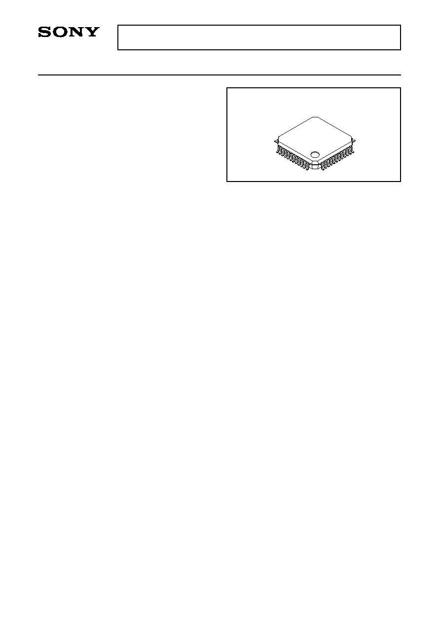
∑ 48-pin QFP package
Structure
Silicon gate CMOS IC
10-bit 85MSPS 3-Channel D/A Converter
48 pin QFP (Plastic)
CXD2309Q
--2--
CXD2309Q
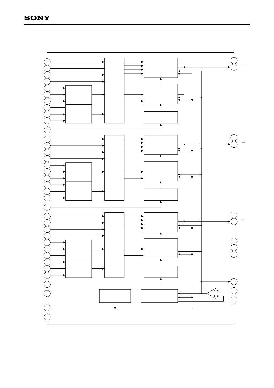
Block Diagram
DECODER
DECODER
LATCHES
4LSB'S
CURRENT
CELLS
DECODER
DECODER
LATCHES
6LSB'S
CURRENT
CELLS
CLOCK
GENERATOR
4LSB'S
CURRENT
CELLS
6LSB'S
CURRENT
CELLS
CLOCK
GENERATOR
DECODER
DECODER
LATCHES
4LSB'S
CURRENT
CELLS
6LSB'S
CURRENT
CELLS
CLOCK
GENERATOR
1
2
3
4
5
6
7
8
9
10
11
12
13
14
15
16
17
18
19
20
31
32
33
48
21
22
23
24
25
26
27
28
29
30
35
34
CURRENT CELLS
(FOR FULL SCALE)
BIAS VOLTAGE
GENERATOR
43
42
44
45
46
47
41
40
39
38
37
36
(LSB) R0
R1
R2
R3
R4
R5
R6
R7
R8
(MSB) R9
RCK
(LSB) G0
G1
G2
G3
G4
G5
G6
G7
G8
(MSB) G9
GCK
(LSB) B0
B1
B2
B3
B4
B5
B6
B7
B8
(MSB) B9
BCK
DV
DD
VB
DV
SS
AV
SS
RO
AV
SS
GO
AV
SS
BO
AV
DD
AV
DD
AV
DD
VG
VREF
IREF
--3--
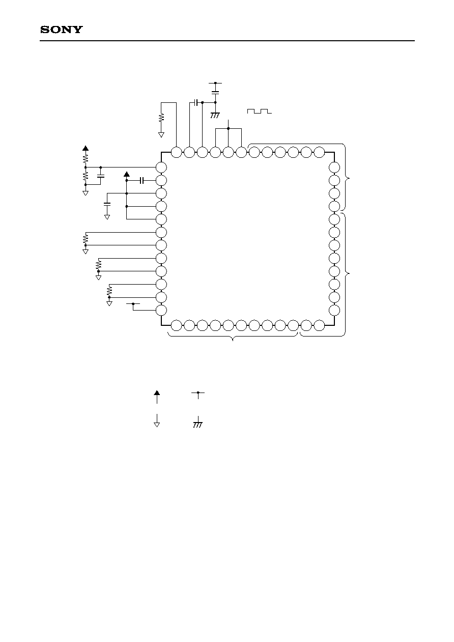
CXD2309Q
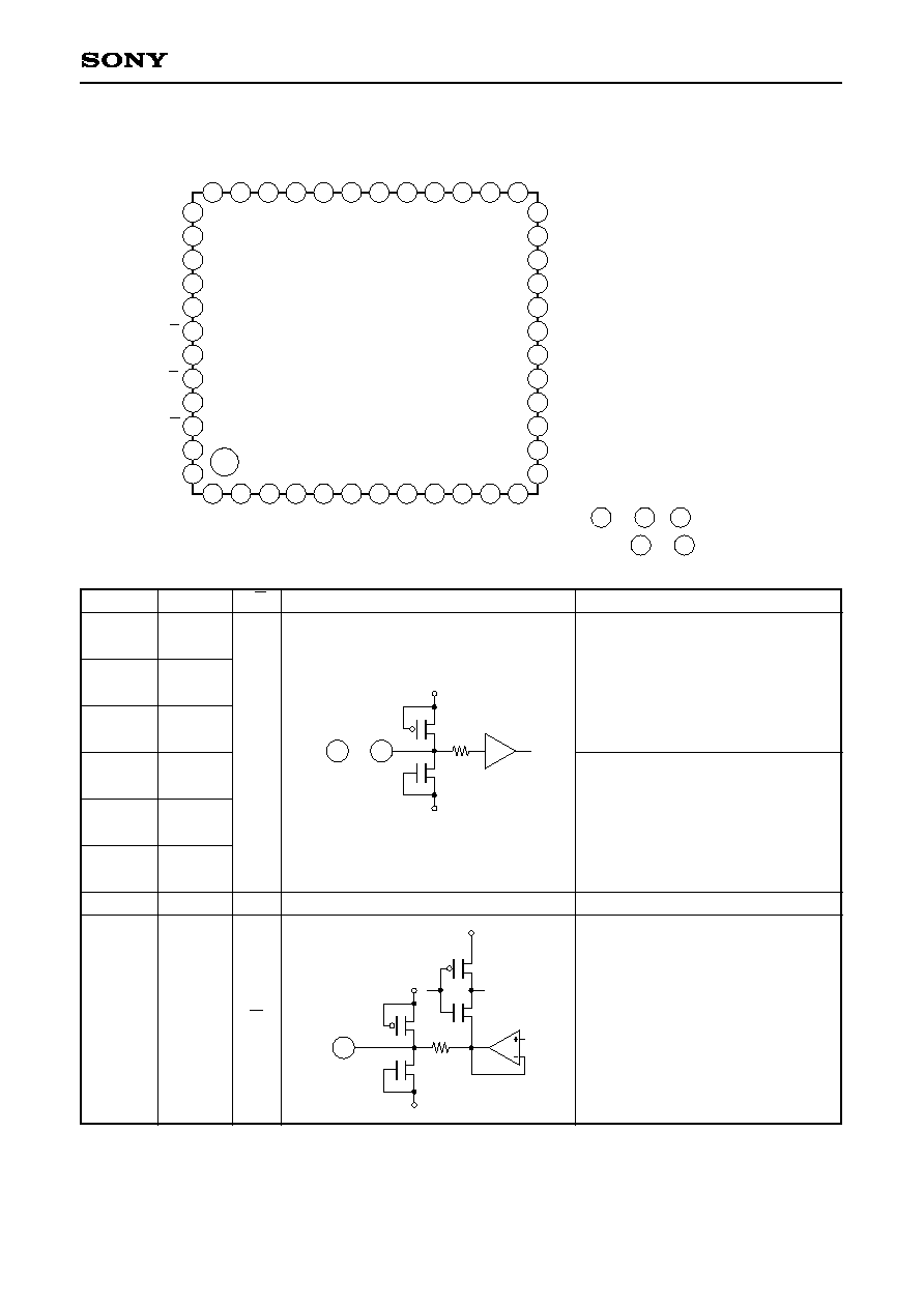
Pin Configuration
2
3
1
4
5
6
7
8
9
10
11
12
22
23
24
21
20
19
18
17
16
15
14
13
35
34
33
32
31
30
29
28
27
26
25
36
46
45
44
43
42
41
40
39
38
47
48
37
(
L
S
B
)
R
0
R
1
R
2
R
3
R
4
R
5
R
6
R
7
R
8
(
M
S
B
)
R
9
(
L
S
B
)
G
0
G
1
I
R
E
F
V
B
D
V
S
S
B
C
K
G
C
K
R
C
K
B
9
(
M
S
B
)
B
8
B
7
B
6
B
5
B
4
B3
B2
B1
B0 (LSB)
G9 (MSB)
G8
G7
G6
G5
G4
G3
G2
1
35 , 48
36
47
to
to
Digital system
Analog system
VG
AV
DD
AV
DD
AV
DD
RO
AV
SS
GO
AV
SS
BO
AV
SS
DV
DD
VREF
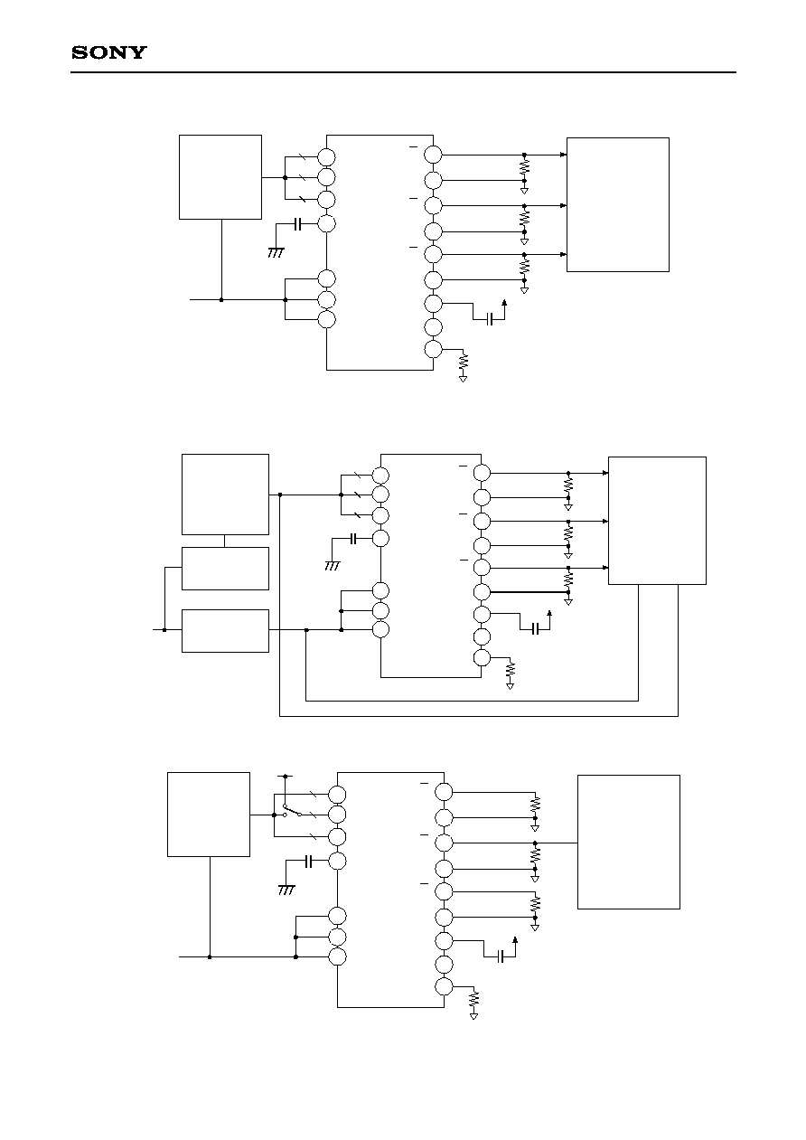
Pin Description and Equivalent Circuit
Pin No.
Symbol
I/O
Equivalent circuit
Description
1 to 10
11 to 20
21 to 30
31
32
33
34
35
R0 to R9
G0 to G9
B0 to B9
RCLK
GCLK
BCLK
DV
SS
VB
I
--
O
DV
DD
DV
SS
33
1
to
Digital input.
1 pin R0 (LSB) to 10 pin R9 (MSB)
11 pin G0 (LSB) to 20 pin G9 (MSB)
21 pin B0 (LSB) to 30 pin B9 (MSB)
Clock input.
Digital ground.
Connect an approximately 0.1µF
capacitor.
DV
DD
DV
SS
35
DV
DD
--4--
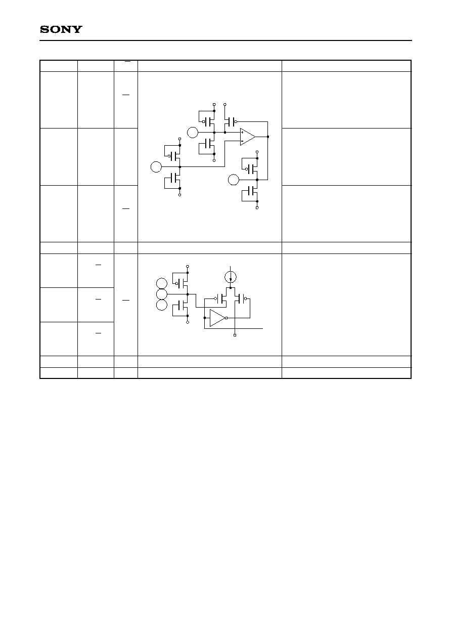
CXD2309Q
Pin No.
Symbol
I/O
Equivalent circuit
Description
36
37
38
39 to 41
42
44
46
43, 45, 47
48
IREF
VREF
VG
AV
DD
RO
GO
BO
AV
SS
DV
DD
O
I
O
--
O
--
--
AV
DD
AV
SS
AV
DD
AV
SS
37
36
AV
DD
AV
DD
AV
SS
38
AV
DD
AV
SS
44
46
42
AV
SS
Reference current output.
Connect an "R
IR
" resistor which are
16 times the output resistance
"R
OUT
".
Reference voltage input.
Sets an output full-scale value.
Connect an approximately 0.1µF
capacitor.
Analog power supply.
Current output. Output can be
obtained by connecting a resistor
(200
typ.).
Analog ground.
Digital power supply.

--5--
CXD2309Q
Electrical Characteristics
(f
CLK
=85 MHz, AV
DD
=DV
DD
=5 V, R
OUT
=200
, V
REF
=2.0 V, R
IR
=3.3 k
, Ta=25∞C)
Item
Resolution
Conversion speed
Integral non-linearity error
Differential non-linearity error
Precision guaranteed
output voltage range
Output full-scale voltage
Output full-scale ratio
1
Output full-scale current
Output offset voltage
Glitch energy
Crosstalk
SN ratio
Supply current
Analog input resistance
Input capacitance
Output capacitance
Digital input voltage
Digital input current
Setup time
Hold time
Propagation delay time
Rise time
Fall time
Symbol
n
f
CLK
E
L
E
D
V
OC
V
FS
F
SR
I
FS
V
OS
GE
CT
SNR
I
DD
R
IN
C
I
C
O
V
IH
V
IL
I
IH
I
IL
ts
th
t
PD
tr
tf
Measurement conditions
AV
DD
=DV
DD
=4.75 to 5.25 V
Ta=≠20 to +85 ∞C
Endpoint
When "0000000000" data input
R
OUT
=100
, 1 Vp-p output
When 10 MHz
F
CLK
=50 MHz
sin wave input
F
CLK
=85 MHz
When 1 MHz
F
CLK
=50 MHz
sin wave input
F
CLK
=85 MHz
When 10 MHz
F
CLK
=50 MHz
sin wave output
F
CLK
=85 MHz
VREF
AV
DD
=DV
DD
=4.75 to 5.25 V
Ta=≠20 to +75 ∞C
AV
DD
=DV
DD
=4.75 to 5.25 V
Ta=≠20 to +75 ∞C
Min.
0
≠2.0
≠0.5
1.8
1.8
0
9.0
40
50
1
2.15
≠5
4
1
Typ.
10
1.92
1.92
9.6
50
42
40
55
50
48
55
125
14
26.5
26.0
Max.
85
2.0
0.5
2.0
2.0
3
10
1
58
9
0.85
5
Unit
bit
MSPS
LSB
LSB
V
V
%
mA
mV
pV∑s
dB
dB
mA
M
pF
pF
V
µA
ns
ns
ns
ns
ns
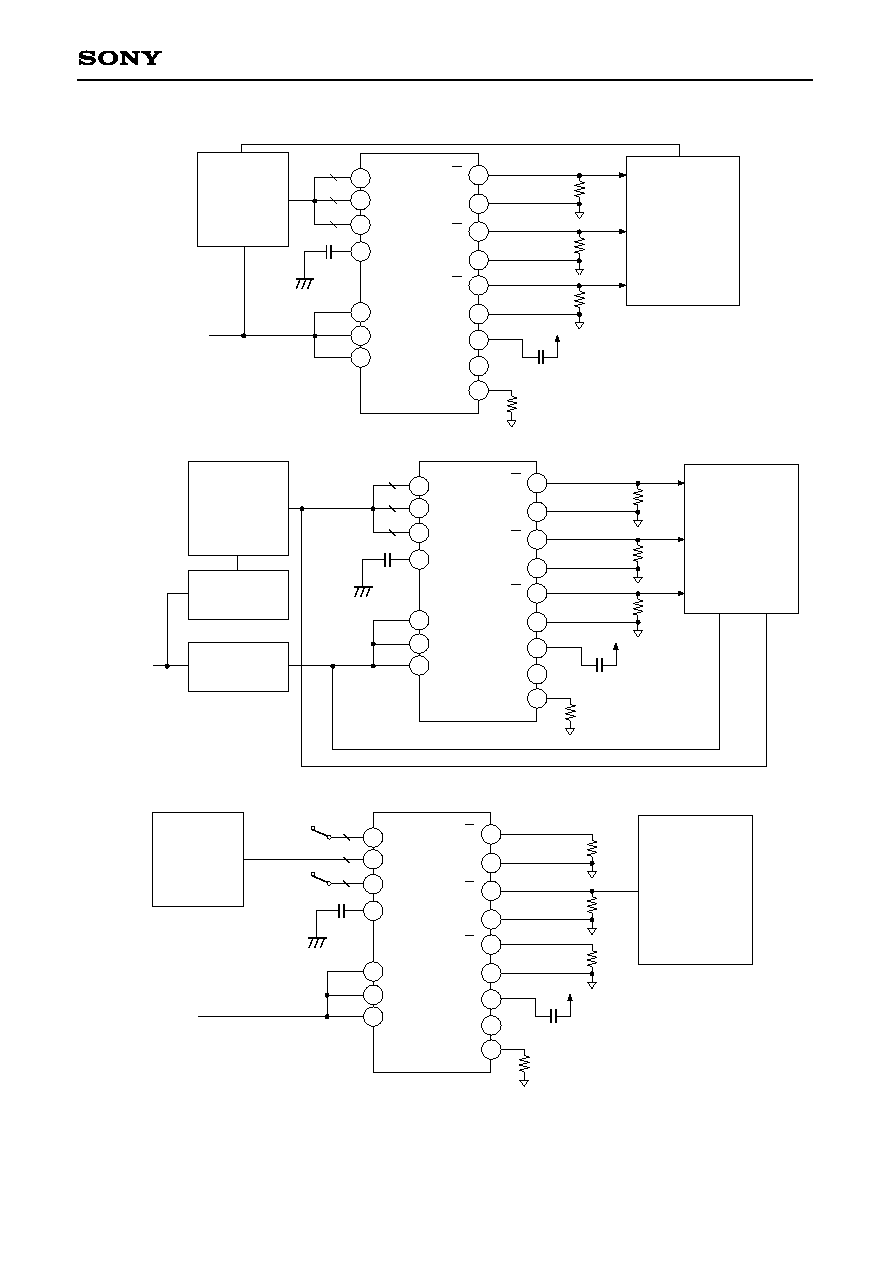
Electrical Characteristics Measurement Circuit
Analog Input Resistance
Measurement Circuit
Digital Input Current
CXD2309Q
+5.25V
AV
DD
, DV
DD
AV
SS
, DV
SS
V
A
}
Full-scale voltage of channel
1
Full-scale output ratio =
Average of the full-scale voltage of the channels
≠1
◊
100 (%)
--6--
CXD2309Q
35
31
32
33
42
43
44
45
46
47
38
37
36
2V
10bit
COUNTER
with
LATCH
OSCILLOSCOPE
CLK
50MHz
SQUARE
WAVE
RO
AV
SS
GO
AV
SS
BO
AV
SS
VG
VREF
IREF
0.1µ
0.1µ
DV
SS
200
200
200
AV
SS
AV
SS
AV
SS
AV
DD
3.3k
AV
SS
VB
RCK
GCK
BCK
R0 to R9
1 to 10
G0 to G9
11 to 20
B0 to B9
21 to 30
Crosstalk Measurement Circuit
35
31
32
33
42
43
44
45
46
47
37
36
2V
DIGITAL
WAVEFORM
GENERATOR
CLK
50MHz
SQUARE
WAVE
DV
DD
DV
SS
0.1µ
RO
AV
SS
GO
AV
SS
BO
AV
SS
VG
VREF
IREF
200
200
200
AV
SS
AV
SS
AV
SS
AV
DD
0.1µ
AV
SS
3.3k
VB
RCK
GCK
BCK
R0 to R9
1 to 10
G0 to G9
11 to 20
B0 to B9
21 to 30
38
SPECTRUM
ANALYZER
Setup Time
Hold Time
Measurement Circuit
Glitch Energy
35
31
32
33
42
43
44
45
46
47
38
37
36
2V
10bit
COUNTER
with
LATCH
DELAY
CONTROLLER
CLK
50MHz
SQUARE
WAVE
OSCILLOSCOPE
VB
RCK
GCK
BCK
DV
SS
0.1µ
RO
AV
SS
GO
AV
SS
BO
AV
SS
VG
VREF
IREF
200
200
200
AV
SS
AV
SS
AV
SS
AV
DD
0.1µ
3.3k
AV
SS
DELAY
CONTROLLER
R0 to R9
1 to 10
G0 to G9
11 to 20
B0 to B9
21 to 30
}
Conversion Rate Measurement Circuit
--7--
CXD2309Q
DC Characteristics Measurement Circuit
35
31
32
33
42
43
44
45
46
47
38
37
36
DVM
CLK
50MHz
SQUARE
WAVE
DV
SS
0.1µ
0.1µ
2V
AV
SS
AV
SS
AV
DD
AV
SS
AV
SS
200
200
200
RO
AV
SS
AV
SS
AV
SS
GO
BO
VG
VREF
IREF
CONTROLLER
3.3k
R0 to R9
1 to 10
VB
RCK
GCK
BCK
G0 to G9
11 to 20
B0 to B9
21 to 30
Propagation Delay Time Measurement Circuit
SNR Measurement Circuit
200
35
31
32
33
42
43
44
45
46
47
38
37
36
10bit
COUNTER
with
LATCH
DELAY
CONTROLLER
DELAY
CONTROLLER
CLK
50MHz
SQUARE
WAVE
DV
SS
OSCILLOSCOPE
0.1µ
0.1µ
RO
AV
SS
AV
SS
AV
SS
GO
BO
VG
VREF
IREF
200
AV
SS
AV
SS
AV
SS
200
AV
DD
2V
3.3k
AV
SS
VB
RCK
GCK
BCK
R0 to R9
1 to 10
G0 to G9
11 to 20
B0 to B9
21 to 30
35
31
32
33
42
43
44
45
46
47
38
37
36
DIGITAL
WAVEFORM
GENERATOR
CLK
50MHz
SQUARE
WAVE
ALL "1"
ALL "1"
0.1µ
DV
SS
200
200
200
AV
SS
AV
SS
AV
SS
AV
DD
0.1µ
2V
3.3k
AV
SS
RO
AV
SS
AV
SS
AV
SS
GO
BO
VG
VREF
IREF
VB
RCK
GCK
BCK
R0 to R9
1 to 10
G0 to G9
11 to 20
B0 to B9
21 to 30
SPECTRUM
ANALYZER
--8--
CXD2309Q
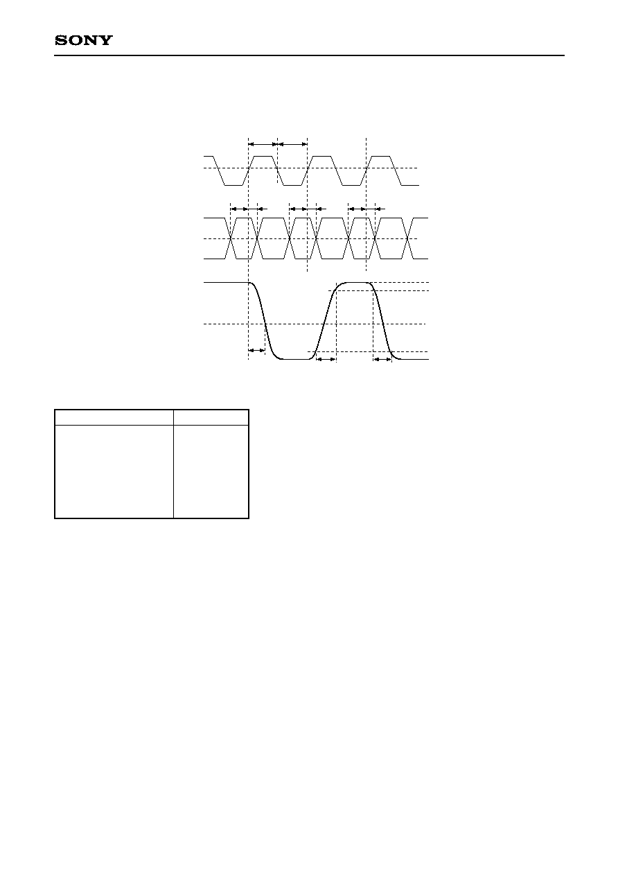
Description of Operation
Timing Chart
I/O Correspondence Table (output full-scale voltage: 2.00 V)
CLK
DATA
D/A OUT
t
PW1
t
PW0
1.5V
t
s
t
h
t
s
t
h
t
s
t
h
t
PD
tr
100%
50%
0%
90%
tf
10%
1.5V
Input code
MSB LSB
1 1 1 1 1 1 1 1 1 1
:
1 0 0 0 0 0 0 0 0 0
:
0 0 0 0 0 0 0 0 0 0
Output voltage
2.0 V
1.0 V
0 V

--9--
CXD2309Q
Notes on Operation
∑ Selecting the Output Resistance
CXD2309Q is a current output type D/A converter. The output voltage can be obtained by connecting the
resistor R
OUT
to the current output pins RO, GO and BO.
Specifications:
Output full-scale voltage V
FS
= 1.8 to 2.0 [V]
Output full-scale current I
FS
= 9.0 to 10.0 [mA]
Calculate the output resistance from V
FS
= I
FS
◊
R
OUT
. Connect a resistance sixteen times the output
resistance to the reference current output pin IREF. In some cases, as this value may not exist, a similar
value can be used instead.
Note that the V
FS
will be the following.
V
FS
= V
REF
◊
16R
OUT
/R
IR
V
REF
is the voltage set at the reference voltage input pin VREF, R
OUT
is the resistor to be connected to the
current output pins RO, GO, BO and R
IR
is the resistor to be connected to the IREF. Power consumption can
be reduced by increasing the resistance, but this will on the contrary increase the glitch energy and data
setting time. Set the best values according to the purpose of use.
∑ Correlation between Data and Clock
For CXD2309Q to display the desired performance as a D/A converter, the data transmitted from outside and
the clock must be synchronized properly. Adjust the setup time (ts) and hold time (th) as specified in
"Electrical Characteristics".
∑ Power supply, ground
Separate the analog and digital signals around the device to reduce noise effects. Bypass the power supply
pin to each ground with a 0.1 µF ceramics capacitor as near as possible to the pin for both the digital and
analog signals.
∑ Latch up
Analog and digital power supplies must be able to share the same power supply of the board. This is to
prevent latch up caused by potential difference between the two pins when the power is turned on.
∑ IREF
The I
REF
pin is very sensitive to improve the AC characteristics. Pay attention for capacitance component not
to attach to this pin because its output may become unstable.
∑ VG pin
It is recommended to use a 1 µF capacitor to improve the AC characteristics though the typical capacitance
value externally connected to the VG pin is 0.1 µF.
∑ Output full-scale voltage
For the applications using the RGB signal, the color balance may be broken up when the RO, GO and BO
output full-scale voltages are used with not adjustment.
--10--
CXD2309Q
∑ When the power supply (AV
DD
and DV
DD
) is 5.0 V.
∑ R1=200
∑ R2=3.3 k
∑ R3=3.0 k
∑ R4=2.0 k
∑ C=0.1 µF
Application Circuit
R2
C
C
Clock input
B ch input
LSB
G ch input
R ch
input
L
S
B
L
S
B
R3
R4
C
C
C
R1
R1
R1
37
38
39
40
41
42
43
44
45
46
47
48
1
2
3
4
5
6
7
8
9
10
11
12
24
23
22
21
20
19
18
17
16
15
14
13
25
26
27
28
29
30
31
32
33
34
35
36
AV
DD
AV
SS
DV
DD
DV
SS
M
S
B
MSB
M
S
B
Application circuits shown are typical examples illustrating the operation of the devices. Sony cannot assume responsibility for
any problems arising out of the use of these circuits or for any infringement of third party patent and other right due to same.
--11--
CXD2309Q
AV
SS
33
C
C
31
+5V
DIGITAL IC
DV
DD
CXD2309Q
39
40
41
AV
DD
DV
DD
DV
SS
AV
SS
34
48
47
45
43
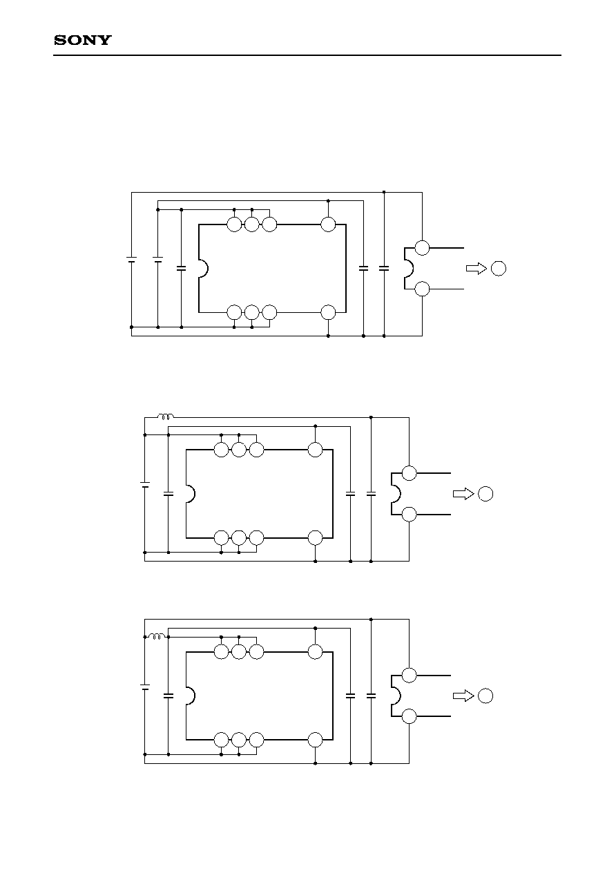
Latch Up Prevention
The CX2309Q is a CMOS IC which requires latch up precautions. Latch up is mainly generated by the lag in
the voltage rising time of AV
DD
(Pin 39, 40 and 41) and DV
DD
(Pin 48), when power supply is ON.
1. Correct usage
a. When analog and digital supplies are from different sources
b. When analog and digital supplies are from a common source
(i)
(ii)
CXD2309Q
AV
SS
AV
DD
39
40
41
AV
DD
DV
DD
DV
SS
AV
SS
C
C
34
+5V
+5V
48
DIGITAL IC
DV
DD
45
47
43
AV
SS
C
C
+5V
DIGITAL IC
DV
DD
CXD2309Q
39
40
41
AV
DD
DV
DD
DV
SS
AV
SS
34
48
45
47
43
--12--
CXD2309Q
2. Example when latch up easily occurs
a. When analog and digital supplies are from different sources
b. When analog and digital supplies are from common source
(i)
(ii)
AV
SS
AV
DD
C
C
+5V
+5V
DIGITAL IC
DV
DD
CXD2309Q
39
40
41
AV
DD
DV
DD
DV
SS
AV
SS
34
48
47
45
43
AV
SS
C
C
+5V
DIGITAL IC
DV
DD
AV
DD
CXD2309Q
39
40
41
AV
DD
DV
DD
DV
SS
AV
SS
34
48
47
45
43
AV
SS
C
+5V
DIGITAL IC
DV
DD
AV
DD
CXD2309Q
39
40
41
AV
DD
DV
DD
DV
SS
AV
SS
34
48
47
45
43
--13--
CXD2309Q
Example of Representative Characteristics
Fig. 1. Reference voltage vs. Output full-scale voltage
O
u
t
p
u
t
f
u
l
l
-
s
c
a
l
e
v
o
l
t
a
g
e
V
F
S
[
V
]
2.0
1.0
Reference voltage V
REF
[V]
1.0
2.0
0
Fig. 2. Output resistance vs. Glitch energy
G
l
i
t
c
h
e
n
e
r
g
y
G
E
[
p
V
∑
s
] 100
50
Output resistance R
OUT
[
]
100
200
0
Fig. 3. Ambient temperature vs. Output full-scale voltage
1.95
1.90
Ambient temperature Ta [∞C]
25
0
O
u
t
p
u
t
f
u
l
l
-
s
c
a
l
e
v
o
l
t
a
g
e
V
F
S
[
V
]
≠25
0
50
75
V=0.02mV/∞C
Fig. 4. Output frequency vs. Supply current
50
40
Output frequency Fo [MHz]
S
u
p
p
l
y
c
u
r
r
e
n
t
I
D
D
[
m
A
]
60
70
sin wave output
20
10
5
30
40
2
1
42
Standard Measurement Conditions
∑ AV
DD
=DV
DD
=5.0 V
∑ V
REF
=2.0 V
∑ F
CLK
=85 MHZ
∑ R
OUT
=200
∑ R
IR
=3.3 k
∑ Ta=25 ∞C
--14--
CXD2309Q
Fig. 5. Clock frequency vs. Supply current
S
u
p
p
l
y
c
u
r
r
e
n
t
I
D
D
[
m
A
]
40
Clock frequency F
CLK
[MHz]
20
50
10
20
30
50
60
85
I
DD
I
A
[Analog]
I
D
[Digital]
Fig. 6. Clock frequency vs. Supply current
S
u
p
p
l
y
c
u
r
r
e
n
t
I
D
D
[
m
A
]
40
Clock frequency F
CLK
[MHz]
20
50
fout=10MHz sin wave
10
20
30
50
60
85
I
DD
I
A
[Analog]
I
D
[Digital]
Fig. 7. Output frequency vs. Cross talk
C
r
o
s
s
t
a
l
k
C
T
[
d
B
]
40
Output frequency Fo [MHz]
0
sin wave output
10
20
30
50
60
Fig. 8. Output frequency vs. Output level
(Including primary hold characteristics sinx/x)
O
u
t
p
u
t
l
e
v
e
l
[
d
B
m
]
Output frequency Fo [MHz]
0
≠20
≠10
0
fout=1MHz sin wave
1
10
2
5
20
42
1
10
2
5
20
50
Standard Measurement Conditions
∑ AV
DD
=DV
DD
=5.0 V
∑ V
REF
=2.0 V
∑ F
CLK
=85 MHZ
∑ R
OUT
=200
∑ R
IR
=3.3 k
∑ Ta=25 ∞C
--15--
CXD2309Q
S
N
R
[
d
B
]
Output frequency Fo [MHz]
30
40
50
Fig. 9. Output frequency vs. SNR
I
n
p
u
t
c
u
r
r
e
n
t
[
µ
A
]
Input voltage [V]
1
6
0
500
1000
5
Fig. 10. Input terminal V-I characteristics
500
1000
≠1
0
1
10
2
5
20
50
Standard Measurement Conditions
∑ AV
DD
=DV
DD
=5.0 V
∑ V
REF
=2.0 V
∑ F
CLK
=85 MHZ
∑ R
OUT
=200
∑ R
IR
=3.3 k
∑ Ta=25 ∞C
SONY CODE
EIAJ CODE
JEDEC CODE
M
PACKAGE STRUCTURE
PACKAGE MATERIAL
LEAD TREATMENT
LEAD MATERIAL
PACKAGE MASS
EPOXY RESIN
SOLDER / PALLADIUM
PLATING
42/COPPER ALLOY
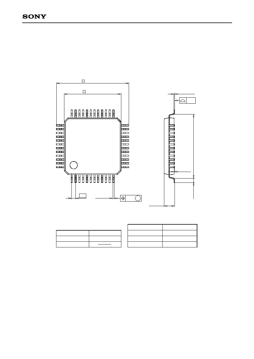
48PIN QFP (PLASTIC)
15.3 ± 0.4
12.0 ≠ 0.1
+ 0.4
0.8
0.3 ≠ 0.1
+ 0.15
0.24
13
24
25
36
37
48
1
12
2.2 ≠ 0.15
+ 0.35
0
.
9
±
0
.
2
0.1 ≠ 0.1
+ 0.2
1
3
.
5
0.15 ≠ 0.05
+ 0.1
QFP-48P-L04
QFP048-P-1212
0.7g
0.15
Package Outline Unit : mm
CXD2309Q
--16--