 | –≠–ª–µ–∫—Ç—Ä–æ–Ω–Ω—ã–π –∫–æ–º–ø–æ–Ω–µ–Ω—Ç: CXD2422R | –°–∫–∞—á–∞—Ç—å:  PDF PDF  ZIP ZIP |
Description
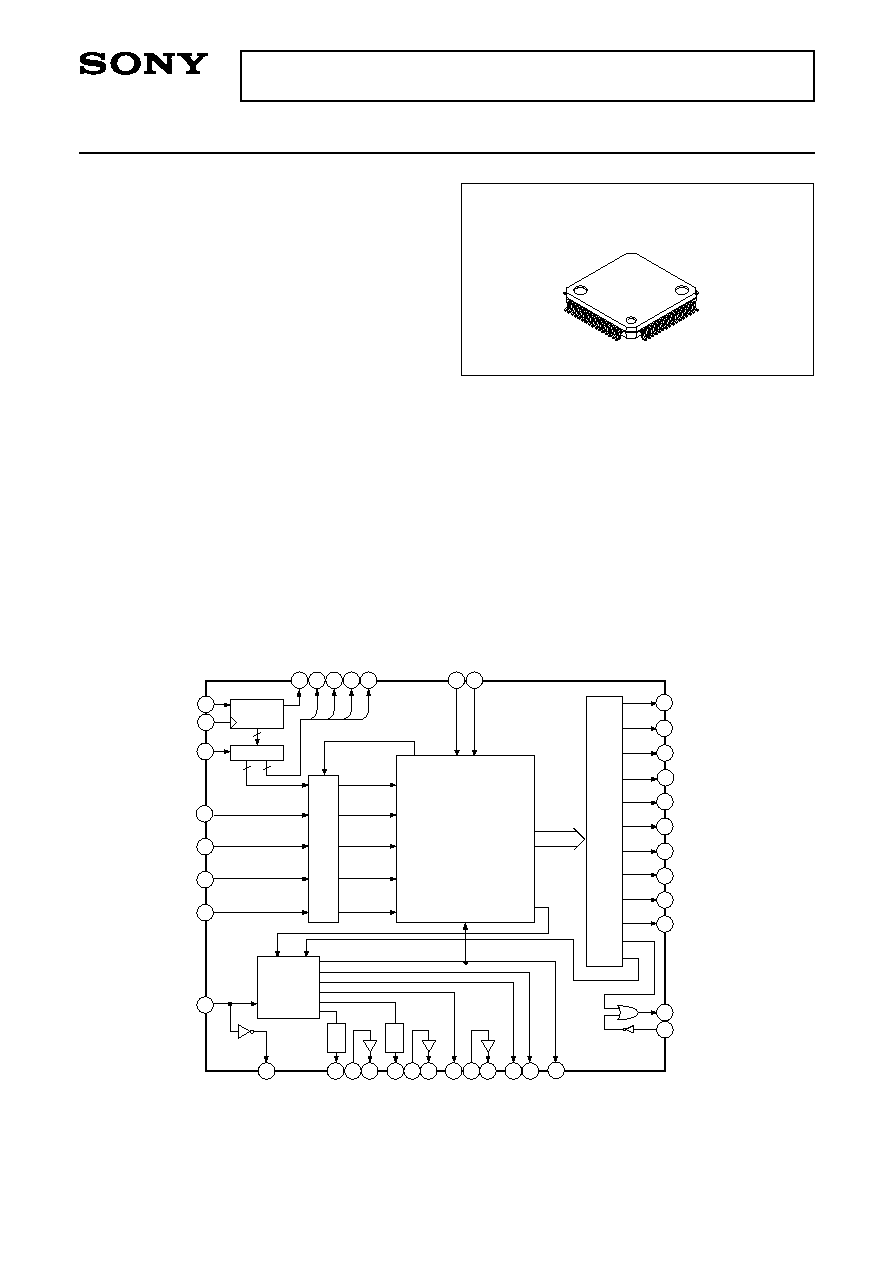
The CXD2422R generates the timing pulses
required for driving and signal processing CCDs with
480,000 pixels (EIA, effective pixels) and CCDs with
570,000 pixels (CCIR, effective pixels).
Features
∑ EIA and CCIR compatible
∑ Compatible with component digital and composite
digital recording format
∑ Compatible with field/frame accumulation modes
Applications
CCD cameras
Structure
Silicon gate CMOS IC
Applicable CCD Image Sensors
ICX062/063AL
Block Diagram
Absolute Maximum Ratings
∑ Supply voltage
V
DD
V
SS
≠ 0.5 to +7.0
V
∑ Input voltage
V
I
V
SS
≠ 0.5 to V
DD
+ 0.5
V
∑ Output voltage
V
O
V
SS
≠ 0.5 to V
DD
+ 0.5
V
∑ Operating temperature
Topr
≠20 to +75
∞C
∑ Storage temperature
Tstg
≠55 to +150
∞C
Recommended Operating Conditions
∑ Supply voltage
V
DD
4.5 to 5.5
V
∑ Operating temperature
Topr
≠20 to +75
∞C
≠ 1 ≠
CXD2422R
E94Y30-ST
CCD Camera Timing Generator
Sony reserves the right to change products and specifications without prior notice. This information does not convey any license by
any implication or otherwise under any patents or other right. Application circuits shown, if any, are typical examples illustrating the
operation of the devices. Sony cannot assume responsibility for any problems arising out of the use of these circuits.
64 pin LQFP (Plastic)
Shift
Register
Latch
Latch
Output
F.F.
High-speed
Pulse
Generation
Circuit
Pulse Generation Circuit
XH gate
Internal clock
PBLK
PBLKON
VD
HD
SD
SC
LD
CLKI
CLKO
CLK
SHP
BAI
BAO
SHD
BBI
BBO
XRG
BCI
BCO
XH1
XH2
D0
SDO
D1
D2
D3
Delay
Delay
V latch
Reset
Shutter data
13
9
4
51 1
2
3
4
5
6
XSG1
39
XSG2
38
XV1
44
XV2
43
XV3
42
XV4
41
XSUB
35
HCLP1
26
HCLP2
22
VCLP
21
28
27
7
36
37
52
53
54
20
19
18
16
15
14
34
33
MODE 63
EIA/CCIR 62
FLD/FRM 61
HTSG 58
32
31
30
≠ 2 ≠
CXD2422R
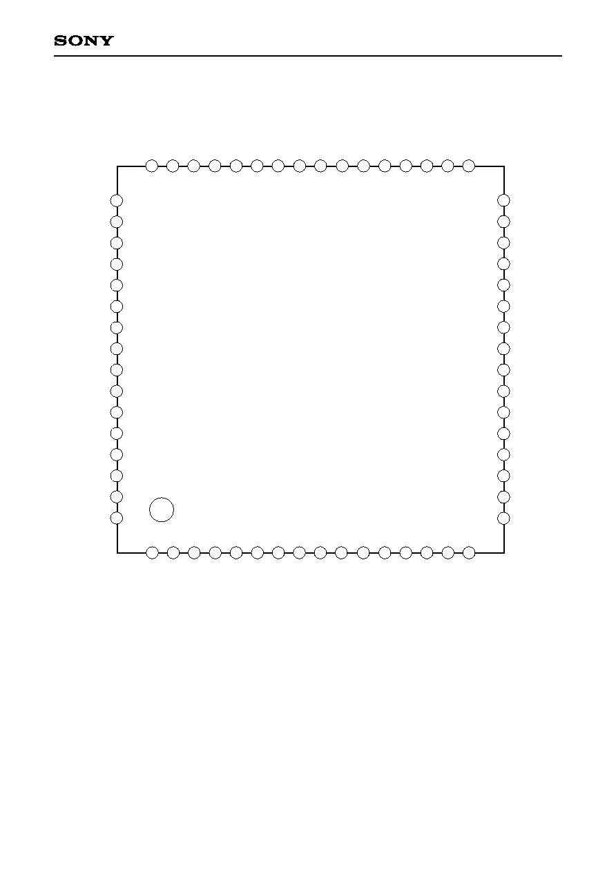
Pin Configuration
NC
BCI
V
DD
NC
HTSG
RST
NC
SDO
BCO
XRG
V
SS
TEST12
FLD/FRM
EIA/CCIR
MODE
TEST13
D0
D1
D2
D3
VD
HD
CLK
V
SS
TEST1
TEST2
TEST3
TEST4
TEST5
NC
SHD
BBI
BBO
VCLP
HCLP2
V
SS
V
DD
TEST6
HCLP1
PBLKON
PBLK
TEST7
SD
SC
LD
TEST11
TEST10
TEST9
TEST8
XV1
XV2
XV3
XV4
V
SS
XSG1
XSG2
XH1
XH2
SHP
BAI
BAO
XSUB
CLKO
CLKI
2
3
4
5
6
7
8
9
10
11
12
13
14
15
16
17
18
19
20
21
22
23
24
25
26
27
28
29
30
40
39
38
37
36
35
34
31
32
33
41
42
43
44
45
46
47
48
49
50
51
52
53
54
55
56
57
58
59
60
63
64
61
62
1
≠ 3 ≠
CXD2422R
Pin Description
Pin No.
Symbol
I/O
Description
1
2
3
4
5
6
7
8
9
10
11
12
13
14
15
16
17
18
19
20
21
22
23
24
25
26
27
28
29
30
31
32
33
34
35
36
37
D0
D1
D2
D3
VD
HD
CLK
V
SS
TEST1
TEST2
TEST3
TEST4
TEST5
SHP
BAI
BAO
(NC)
SHD
BBI
BBO
VCLP
HCLP2
V
SS
V
DD
TEST6
HCLP1
PBLKON
PBLK
TEST7
SD
SC
LD
CLKI
CLKO
XSUB
XH2
XH1
O
O
O
O
I
I
O
--
I
I
I
I
I
O
I
O
--
O
I
O
O
O
--
--
I
O
I
O
I
I
I
I
I
O
O
O
O
Extended I/O output.
Extended I/O output.
Extended I/O output.
Extended I/O output.
Vertical sync signal input. (With pull-up resistor)
Horizontal sync signal input. (With pull-up resistor)
Two frequency divider output of Pin 33.
Test input (normally Low). (With pull-down resistor)
Test input (normally Low). (With pull-down resistor)
Test input (normally Low). (With pull-down resistor)
Test input (normally Low). (With pull-down resistor)
Test input (normally Low). (With pull-down resistor)
CCD output precharge level sampling pulse output.
Buffer input (for phase adjustment of SHP). (With pull-up resistor)
Non-inversed output of BAI.
CCD output signal level sampling pulse output.
Buffer input (for phase adjustment of SHD). (With pull-up resistor)
Non-inversed output of BBI.
Vertical clamp pulse output.
Horizontal (dummy bit block) clamp pulse output.
Test input (normally High). (With pull-up resistor)
Horizontal (OPB block) clamp pulse output.
Output ON/OFF of PBLK. (High: ON) (With pull-up resistor).
Preblanking pulse output.
Test input (normally High). (With pull-up resistor)
Serial data input for electronic shutter control. (With pull-up resistor)
Clock input for electronic shutter control. (With pull-up resistor)
Latch pulse input for electronic shutter control. (With pull-up resistor)
Clock input.
Inversed output of CLKI.
Substrate pulse output for electronic shutter.
Clock output for horizontal register drive.
Clock output for horizontal register drive.
≠ 4 ≠
CXD2422R
Pin No.
Symbol
I/O
Description
38
39
40
41
42
43
44
45
46
47
48
49
50
51
52
53
54
55
56
57
58
59
60
61
62
63
64
XSG2
XSG1
V
SS
XV4
XV3
XV2
XV1
TEST8
TEST9
TEST10
TEST11
(NC)
(NC)
SDO
BCO
BCI
XRG
V
SS
V
DD
(NC)
HTSG
RST
TEST12
FLD/FRM
EIA/CCIR
MODE
TEST13
O
O
--
O
O
O
O
O
O
O
O
--
--
O
O
I
O
--
--
--
I
I
I
I
I
I
I
Sensor charge readout pulse output.
Sensor charge readout pulse output.
Clock output for vertical register drive.
Clock output for vertical register drive.
Clock output for vertical register drive.
Clock output for vertical register drive.
Test output (normally open).
Test output (normally open).
Test output (normally open).
Test output (normally open).
Serial data output for electronic shutter control.
Non-inversed output of BCI.
Buffer input (for phase adjustment of XRG). (With pull-up resistor)
Reset gate pulse output of output block.
Readout pulse (XSG1, 2) ON/OFF. (High: OFF) (With pull-down resistor)
Test input (normally High). (With pull-up resistor)
Test input (normally Low). (With pull-up resistor)
High: Field accumulation mode, Low: Frame accumulation mode.
(With pull-up resistor)
High: EIA, Low: CCIR. (With pull-up resistor)
High: Component digital mode, Low: Composite digital mode.
(With pull-up resistor)
Test input (normally Low). (With pull-up resistor)
Note) TEST12 and TEST13 have a built-in pull-up resistor.
Be sure to fix them at Low.
≠ 5 ≠
CXD2422R
Item
Conditions
Min.
Typ.
Max.
Unit
Supply voltage
Input/Output voltages
Input voltage
Output voltage
Pull-up/
Pull-down resistors
Symbol
V
DD
V
I
, V
O
V
IH
V
IL
V
OH
V
OL
R
PU
,
R
PD
I
OH
= ≠2mA
I
OL
= 4mA
V
IL
= 0V, V
IH
= V
DD
4.5
V
SS
0.7V
DD
V
DD
≠ 0.8
40k
5.0
100k
5.5
V
DD
0.3V
DD
0.4
250k
V
V
V
V
V
V
Electrical Characteristics
1) DC characteristics
(V
DD
= 4.5 to 5.5V, Topr = ≠20 to +75∞C)
2) AC characteristics
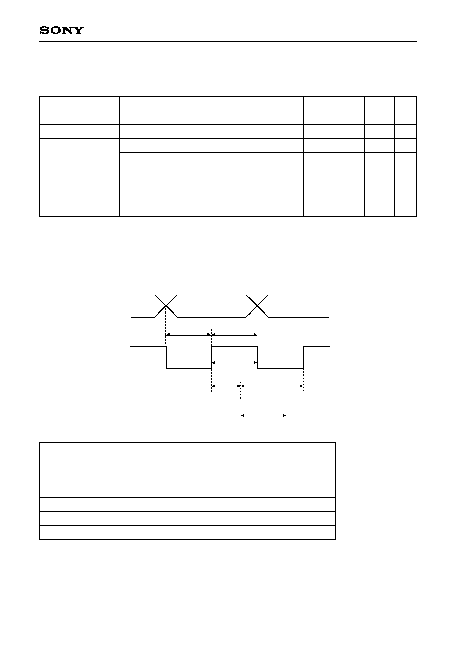
2)-1. Pulses for electronic shutter control (SD, SC, LD)
SD
SC
LD
ts1
t
H
1
tw1
ts2
t
H
2
tw2
Symbol
Item
Min.
t
s1
t
H
1
t
w1
t
s2
t
H
2
t
w2
SD set-up time, activated by the rising edge of SC
SD hold time, activated by the rising edge of SC
SC pulse width
SC set-up time, activated by the rising edge of LD
SC hold time, activated by the rising edge of LD
LD pulse width
20ns
20ns
20ns
20ns
20ns
20ns