 | –≠–ª–µ–∫—Ç—Ä–æ–Ω–Ω—ã–π –∫–æ–º–ø–æ–Ω–µ–Ω—Ç: CXD2452R | –°–∫–∞—á–∞—Ç—å:  PDF PDF  ZIP ZIP |

≠ 1 ≠
CXD2452R
E96830C9X
Timing Generator for Progressive Scan CCD Image Sensor
Description
The CXD2452R is a timing generator which generates
the timing pulses for performing progressive scan
readout for digital still cameras and personal
computer image input applications using the
ICX098AK CCD image sensor.
Features
∑ Base oscillation frequency 36.81MHz (2340f
H
)
∑ Monitoring readout allowed
∑ High-speed/low-speed electronic shutter function
∑ Horizontal driver for CCD image sensor
∑ Signal processor IC system clock generation 1170f
H
,
780f
H
∑ Vertical/horizontal sync (SSG) timing generation
Applications
∑ Digital still cameras
∑ Personal computer image input
Structure
Silicon gate CMOS IC
Pin Configuration
Absolute Maximum Ratings
∑ Supply voltage V
DD
Vss ≠ 0.5 to +7.0
V
∑ Input voltage
V
I
Vss ≠ 0.5 to V
DD
+ 0.5
V
∑ Output voltage V
O
Vss ≠ 0.5 to V
DD
+ 0.5
V
∑ Operating temperature
Topr
≠20 to +75
∞C
∑ Storage temperature
Tstg
≠55 to +150
∞C
Recommended Operating Conditions
∑ Supply voltage
V
DD
a, V
DD
b, V
DD
c, V
DD
d
3.0 to 3.6
V
∑ Operating temperature
Topr
≠20 to +75
∞C
Applicable CCD Image Sensors
ICX098AK (Type 1/4 CCD)
Sony reserves the right to change products and specifications without prior notice. This information does not convey any license by
any implication or otherwise under any patents or other right. Application circuits shown, if any, are typical examples illustrating the
operation of the devices. Sony cannot assume responsibility for any problems arising out of the use of these circuits.
48 pin LQFP (Plastic)
2
3
4
5
6
7
8
9 10 11 12
13
14
15
16
17
18
19
20
21
22
23
24
25
26
27
28
29
30
40
39
38
37
36 35 34
31
32
33
41
42
43
44
45
46
47
48
1
OSCI
3MCK
V
SS
1
WEN
TEST
V
DD
1
XCLPOB
H1
V
SS
2
RG
V
DD
2
V
SS
5
CLD
FRI
HRI
HRO
FRO
EBCKSM
SEN
SSK
SSI
V
DD
6
RST
OSCO
XV1
V
DD
7
XSUB
XV2
XSG2
XV3
V
SS
6
MCK
DSGAT
H2
V
DD
3
V
DD
4
XSHP
XSHD
V
SS
4
1/2MCK
ID
V
SS
3
XCLPDM
XRS
V
DD
5
PBLK
XSG1
3/2MCK
*Groups of pins enclosed in the fingure indicate sections for which power supply separationis possible.
≠ 2 ≠
CXD2452R
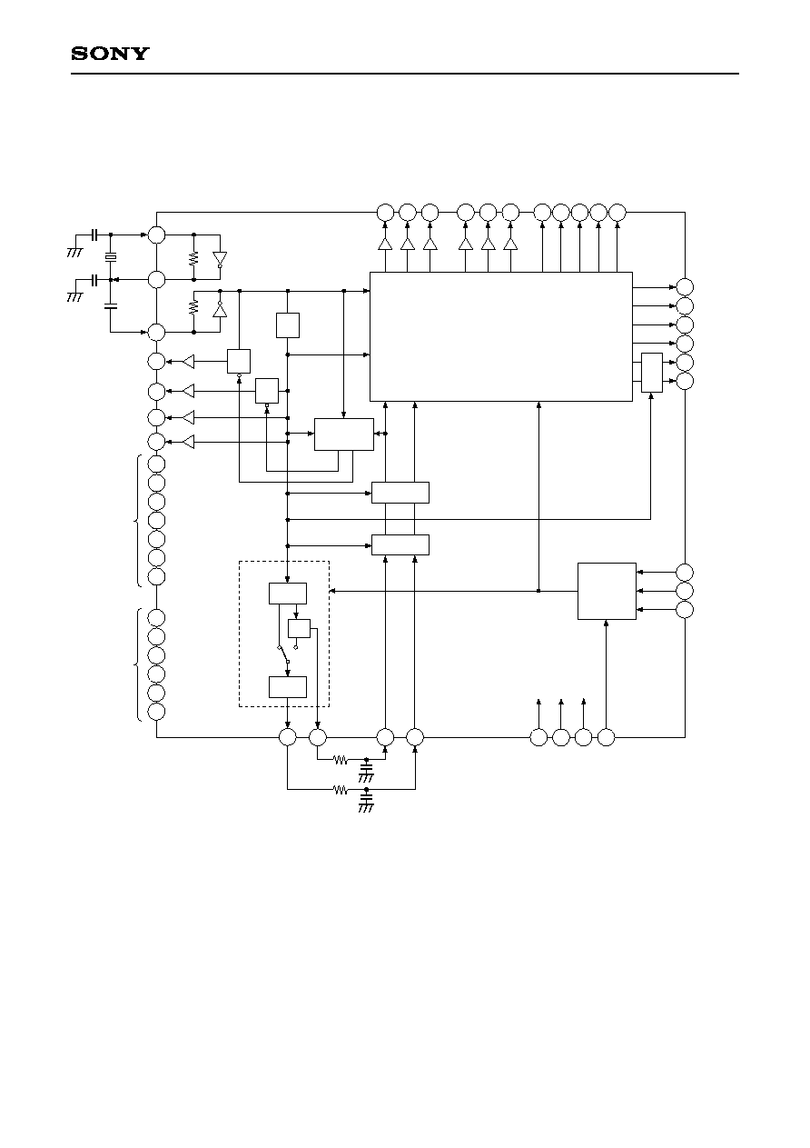
Block Diagram
3
4
7
15
21
30
40
37
34
31
33
WEN
T
E
S
T
XCLPDM
XCLPOB
12
H
1
9
R
G
R
S
T
F
R
I
H
R
I
H
R
O
F
R
O
E
B
C
K
S
M
SEN
SSK
SSI
XSUB
D
S
G
A
T
13
H
2
ID
17
18
19
X
S
H
P
X
S
H
D
X
R
S
PBLK
41
42
43
44
46
X
V
1
X
V
2
X
S
G
2
X
V
3
X
S
G
1
L
a
t
c
h
27
28
29
Latch
Latch
HRI
differential
1/2
1/3
1/2
1/390
1/525
SSG
32
5
Register
Pulse Generator
2
8
10
11
14
16
20
24
26
39
38
35
45
47
48
1
OSCI
3MCK
V
SS
CLD
V
DD
1/2MCK
OSCO
MCK
36
6
25
3/2MCK 23
1/2
22

≠ 3 ≠
CXD2452R
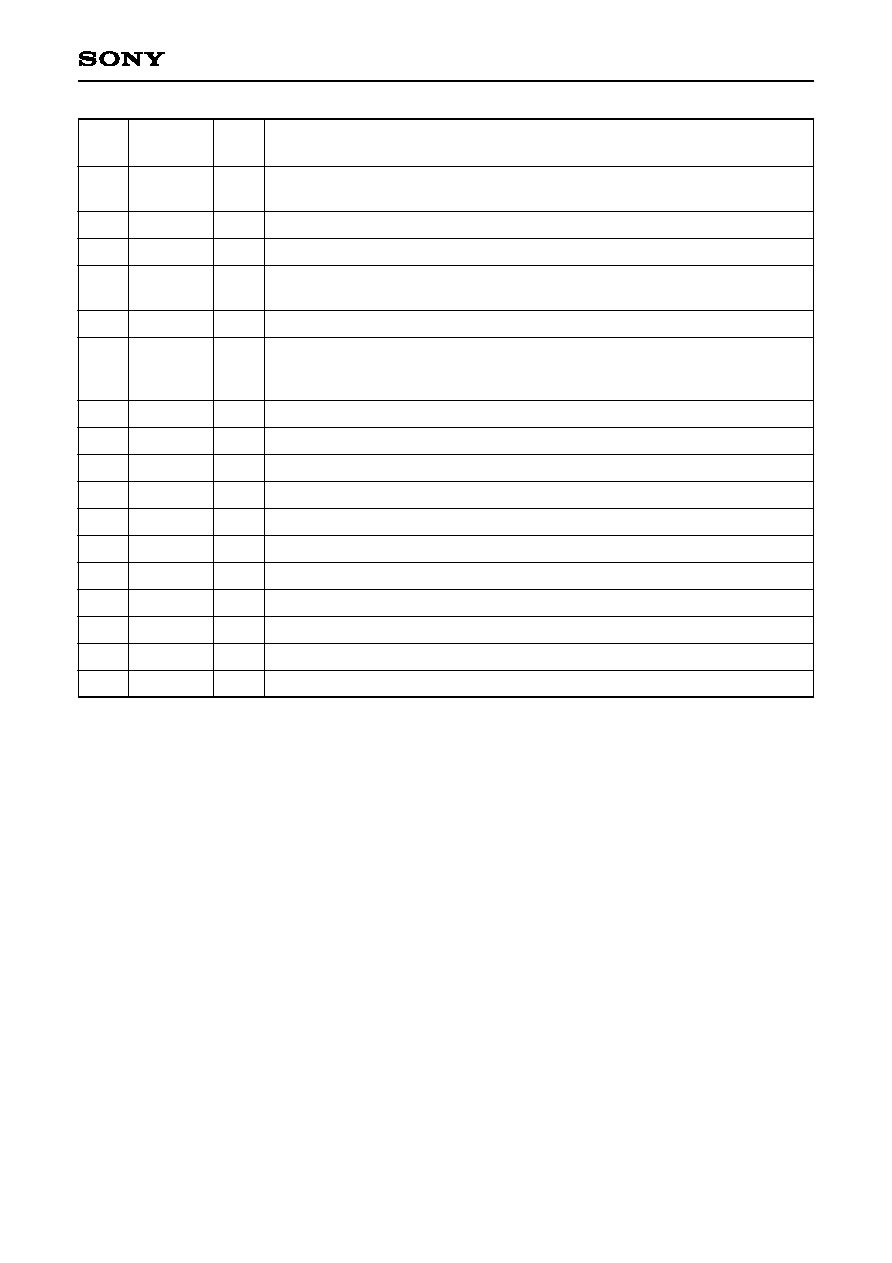
Pin Description
Pin
No.
1
2
3
4
5
6
7
8
9
10
11
12
13
14
15
16
17
18
19
20
21
22
23
24
25
26
27
28
29
30
31
3MCK
Vss1
WEN
ID
TEST
V
DD
1
XCLPOB
V
DD
2
RG
Vss2
Vss3
H1
H2
V
DD
3
XCLPDM
V
DD
4
XSHP
XSHD
XRS
Vss4
PBLK
1/2MCK
3/2MCK
V
DD
5
RST
V
DD
6
SSI
SSK
SEN
EBCKSM
FRO
I
--
O
O
I
--
O
--
O
--
--
O
O
--
O
--
O
O
O
--
O
O
--
--
I
--
I
I
I
I
O
Internal main clock. (2340f
H
)
GND
Memory write timing.
Stop control possible using the serial interface data.
Vertical direction line identification pulse output.
Stop control possible using the serial interface data.
IC test pin; normally fixed to GND. (With pull-down resistor)
3.3V power supply. (Power supply for common logic block)
CCD optical black signal clamp pulse output.
Stop control possible using the serial interface data.
3.3V power supply. (Power supply for RG)
CCD reset gate pulse output. (780f
H
)
GND
GND
CCD horizontal register drive clock output. (780f
H
)
CCD horizontal register drive clock output. (780f
H
)
3.3V power supply. (Power supply for H1/H2)
Pulse output for dummy bit block clamp .
3.3V power supply. (Power supply for CDS system)
Precharge level sample-and-hold pulse output. (780f
H
)
Data level sample-and-hold pulse output. (780f
H
)
Sample-and-hold pulse output for analog/digital conversion phase alignment. (780f
H
)
GND
Pulse output for horizontal and vertical blanking interval pulse cleaning.
Horizontal direction pixel identification pulse output.
Stop control possible using the serial interface data.
System clock output for signal processing IC (1170f
H
).
Stop control possible using the serial interface data.
3.3V power supply. (Power supply for common logic block)
Internal system reset input. High: Normal status, Low: Reset status
Always input one reset pulse after power-on.
3.3V power supply. (Power supply for common logic block)
Serial interface data input for internal mode settings.
Serial interface clock input for internal mode settings.
Serial interface strobe input for internal mode settings.
CHKSUM enable. (With pull-down resistor)
High: Sum check invalid, Low: Sum check valid
Vertical sync signal output.
Stop control possible using the serial interface data.
Symbol
I/O
Description
≠ 4 ≠
CXD2452R
32
33
34
35
36
37
38
39
40
41
42
43
44
45
46
47
48
HRO
HRI
FRI
CLD
V
SS
5
DSGAT
MCK
Vss6
XSUB
XV3
XSG2
XSG1
XV2
V
DD
7
XV1
OSCO
OSCI
O
I
I
O
--
I
O
--
O
O
O
O
O
--
O
O
I
Horizontal sync signal output.
Stop control possible using the serial interface data.
Horizontal sync signal input.
Vertical sync signal input.
Clock output for analog/digital conversion IC. (780f
H
)
Phase adjustment in 60∞ units possible using the serial interface data.
GND
Control input used to stop pulse generation for CCD image sensor, sample-and-
hold IC and analog/digital conversion IC. High: Normal status, Low: Stop status
Controlled pulse can be changed using the serial interface data.
System clock output for signal processor IC. (780f
H
)
GND
Pulse output for electronic shutter.
CCD vertical register drive pulse output.
CCD sensor readout pulse output.
CCD sensor readout pulse output.
CCD vertical register drive pulse output.
3.3V power supply. (Power supply for common logic block)
CCD vertical register drive pulse output.
Inverter output for oscillation.
Inverter input for oscillation.
Pin
No.
Symbol
I/O
Description
≠ 5 ≠
CXD2452R
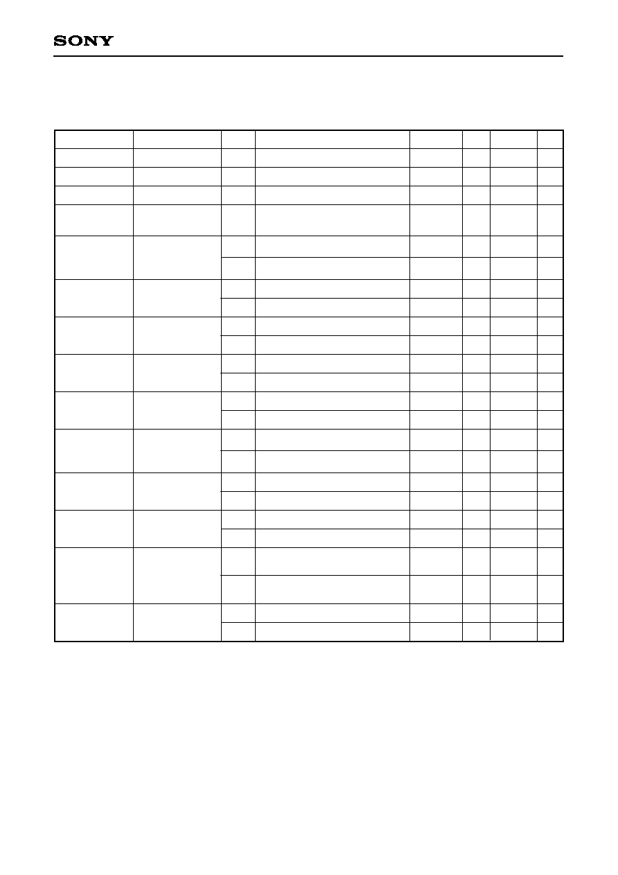
Electrical Characteristics
DC Characteristics
(Within the recommended operating conditions)
Item
Pins
Symbol
Conditions
Min.
Typ.
Max.
Unit
1
These input pins do not have protective diodes on the internal power supply side.
2
These input pins have internal pull-down resistors.
3
The above table indicates the condition for 3.3V drive.
Supply voltage 1
Supply voltage 2
Supply voltage 3
Supply voltage 4
Input voltage 1
1
Input
voltage 2
1
2
Input
voltage 3
2
Output
voltage 1
Output
voltage 2
Output
voltage 3
Output
voltage 4
Output
voltage 5
Output
voltage 6
Output
voltage 7
V
DD
2
V
DD
3
V
DD
4
V
DD
1, V
DD
5,
V
DD
6, V
DD
7
RST, DSGAT,
SSI, SSK, SEN,
FRI, HRI
EBCKSM
TEST
RG
H1, H2
XSHP, XSHD,
XRS, PBLK,
XCLPDM
3/2MCK, MCK,
CLD
1/2MCK
XV1, XV2, XV3,
XSUB, XSG1,
XSG2, XCLPOB,
ID, WEN
FRO, HRO
V
DD
a
V
DD
b
V
DD
c
V
DD
d
V
IH1
V
IL1
V
IH2
V
IL2
V
IH3
V
IL3
V
OH1
V
OL1
V
OH2
V
OL2
V
OH3
V
OL3
V
OH4
V
OL4
V
OH5
V
OL5
V
OH6
V
OL6
V
OH7
V
OL7
3.0
3.0
3.0
3.0
0.8V
DD
d
0.8V
DD
d
0.7V
DD
d
V
DD
a ≠ 0.8
V
DD
b ≠ 0.8
V
DD
c ≠ 0.8
V
DD
d ≠ 0.8
V
DD
d ≠ 0.8
V
DD
d ≠ 0.8
V
DD
d ≠ 0.8
3.3
3.3
3.3
3.3
3.6
3.6
3.6
3.6
0.2V
DD
d
0.2V
DD
d
0.3V
DD
d
0.4
0.4
0.4
0.4
0.4
0.4
0.4
V
V
V
V
V
V
V
V
V
V
V
V
V
V
V
V
V
V
V
V
V
V
V
V
Feed current where I
OH
= ≠3.3mA
Pull-in current where I
OL
= 2.4mA
Feed current where I
OH
= ≠10.4mA
Pull-in current where I
OL
= 7.2mA
Feed current where I
OH
= ≠3.3mA
Pull-in current where I
OL
= 2.4mA
Feed current where I
OH
= ≠10.4mA
Pull-in current where I
OL
= 7.2mA
Feed current where I
OH
= ≠3.3mA
Pull-in current where I
OL
= 2.4mA
Feed current where I
OH
= ≠2.4mA
Pull-in current where I
OL
= 4.8mA
Feed current where I
OH
= ≠3.6mA
Pull-in current where I
OL
= 7.2mA