 | –≠–ª–µ–∫—Ç—Ä–æ–Ω–Ω—ã–π –∫–æ–º–ø–æ–Ω–µ–Ω—Ç: CXD2508AR | –°–∫–∞—á–∞—Ç—å:  PDF PDF  ZIP ZIP |
Description
The CXD2508AQ/AR is a digital signal processor
for CD players and is equipped with built-in digital
filters, no-sound data detection circuit, and 1-bit
DAC.
Features
DSP block
∑ Digital PLL
∑ EFM frame sync protection
∑ SEC strategy-based error correction
∑ Subcode demodulation, CRC checking
∑ Digital spindle servo
∑ Servo auto sequencer
∑ Asymmetry compensation circuit
∑ Digital audio interface output
∑ 16K RAM
∑ Double-speed playback capability
∑ New microcomputer interface circuit
Digital filter, DAC block
∑ Double-speed playback capability
∑ Digital de-emphasis
∑ Digital attenuation
∑ No-sound data detection circuit
∑ 4 Fs oversampling filter
∑ Secondary
noise shaper
∑ PWM-system pulse conversion output
Recommended Operating Conditions
∑ Supply voltage V
DD Note)
4.5 to 5.5V
(double-speed playback)
3.5 to 5.5V
(normal-speed playback)
3.4 to 5.5V
(low power consumption
or special playback mode)
∑ Operating temperature
Topr
≠20 (min.)
75 (max.)
∞C
Note) V
DD
(min.) is varied by the playback speed and built-in
VCO in the CXD2508AQ/AR. 4.5V is the value using the
VCO which generates the slower frequency in double-
speed playback. The table below shows the V
DD
(min.)
for each condition.
When the internal operation of the LSI is set to double-
speed mode and the crystal oscillation frequency is
halved, normal-speed playback results.
Applications
CD players
Structure
Silicon gate CMOS IC
Absolute Maximum Ratings
∑ Supply voltage
V
DD
≠0.3 to 7.0
V
∑ Input voltage
V
I
≠0.3 to 7.0
V
∑ Input voltage
V
IN
Vss≠0.3V (min.) V
DD
+0.3 (max.) V
∑ Output voltage
V
O
≠0.3 to 7.0
V
∑ Storage temperature
Tstg
≠40 to 125
∞C
∑ Supply voltage variation
V
SS
≠AV
SS
≠0.3V (min.) +0.3V (max.)
V
DD
≠AV
DD
≠0.3V (min.) +0.3V (max.)
≠ 1 ≠
CXD2508AQ/AR
E94602A54-ST
CD Digital Signal Processor
Sony reserves the right to change products and specifications without prior notice. This information does not convey any license by
any implication or otherwise under any patents or other right. Application circuits shown, if any, are typical examples illustrating the
operation of the devices. Sony cannot assume responsibility for any problems arising out of the use of these circuits.
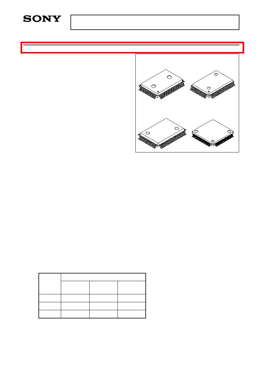
CXD2508AQ
80 pin QFP (Plastic)
CXD2508AQ
80 pin QFP (Plastic)
CXD2508AR
80 pin LQFP (Plastic)
CXD2508AQ
80 pin QFP (Plastic)
Playback
speed
VCO
high-speed
VCO
normal-speed
DAC block
◊
2
3.40
4.50
3.40
◊
1
3.40
3.50
3.40
◊
1
3.40
3.40
3.40
V
DD
(min.) [V]
For the availability of this product, please contact the sales office.
≠ 2 ≠
CXD2508AQ/AR
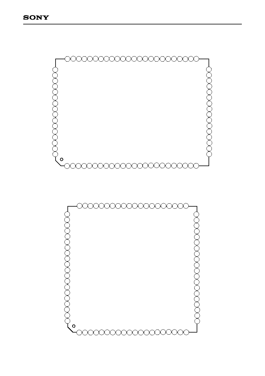
Pin Configuration
WFCK
EMPHI
EMPH
DOUT
C4M
FSTT
MNT0
MNT1
MNT3
XROF
C2PO
Vss
RFCK
GFS
XPCK
XUGF
GTOP
BCKI
BCK
PCMDI
PCMD
LRCKI
LRCK
WDCK
SCOR
SBSO
EXCK
SQSO
SQCK
MUTE
SENS
XRST
DATA
XLAT
CLOK
Vss
SEIN
CNIN
DATO
XLTO
CLKO
SPOA
SPOB
SPOC
XTSL
XLON
FOK
MON
ASYE
ASYO
ASYI
BIAS
RF
AV
DD
1
CLTV
AVss1
V
DD
PCO
FILI
FILO
TEST
LOCK
MDS
MDP
70
69
68
67
65
66
71
72
73
74
75
76
77
78
79
80
16 17 18
2
3
4
5
6
7
8
9 10 11 12 13 14 15
19 20 21 22 23 24
1
ZEROL
ZEROR
DTS1
V
DD
NLPWM
LPWM
AV
DD
2
AV
DD
3
XTAI
XTAO
AVss3
AVss2
NRPWM
RPWM
DTS2
DTS3
25
26
27
28
29
30
40
39
38
37
36
35
34
31
32
33
41
42
43
44
45
46
47
48
49
50
51
52
53
54
55
56
57
58
59
60
63
64
61
62
CXD2508AQ
EMPHI
WFCK
ZEROL
ZEROR
DTS1
V
DD
NLPWM
LPWM
AV
DD
2
AV
DD
3
XTAI
XTAO
AVss3
AVss2
NRPWM
RPWM
DTS2
DTS3
SCOR
SBSO
EMPH
DOUT
C4M
FSTT
MNT0
MNT1
MNT3
XROF
C2PO
Vss
RFCK
GFS
XPCK
XUGF
GTOP
BCKI
BCK
PCMDI
PCMD
LRCKI
EXCK
SQSO
SQCK
MUTE
SENS
XRST
DATA
XLAT
CLOK
Vss
SEIN
CNIN
DATO
XLTO
CLKO
SPOA
SPOB
SPOC
XTSL
XLON
16 17 18
2
3
4
5
6
7
8
9 10 11 12 13 14 15
19 20
1
41
42
43
44
45
46
47
48
49
50
51
52
53
54
55
56
57
58
59
60
70
69
68
67
65
66
71
72
73
74
75
76
77
78
79
80
63
64
61
62
CXD2508AR
LRCK
WDCK
ASYE
ASYO
ASYI
BIAS
RF
AVdd1
CLTV
AVss1
Vdd
PCO
FILI
FILO
TEST
LOCK
MDS
MDP
MON
FOK
21
22
23
24
25
26
27
28
29
30
40
39
38
37
36
35
34
31
32
33
≠ 3 ≠
CXD2508AQ/AR
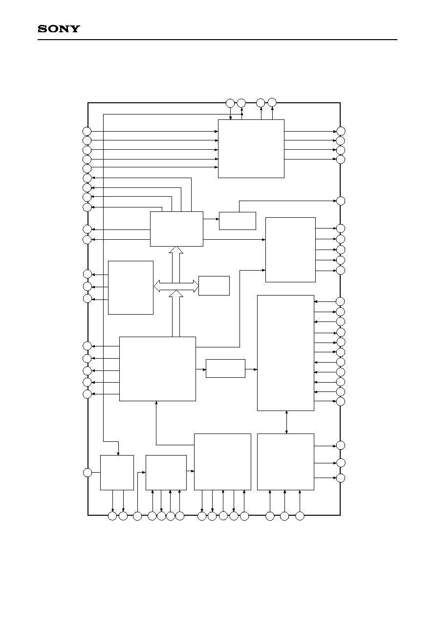
Block Diagram
2
3
4
5
6
7
9
10
11
13
14
15
16
17
18
19
22
23
24
25
26
27
29 30
40
39
38
37
36
34
31
41
42
43
44
45
46
47
48
49
50
51
52
54
55
56
57
58
59
60
70
69
63
64
65
66
61
62
73 74
77
78
1
SQCK
SQSO
EXCK
SBSO
SCOR
XLON
SPOA to C
CLOK
XLAT
DATA
SENS
CLKO
XLTO
DATO
XROF
LOCK
MDS
MDP
MON
DOUT
NLPWM
LPWM
RPWM
NRPWM
FOK
SEIN
CNIN
XPCK
FILO
FILI
PCO
CLTV
ASYI
ASYO
ASYE
BIAS
FSTT
C4M
RF
XTSL
WFCK
EMPH
GFS
XUGF
GTOP
MNT0
MNT1
MNT3
C2PO
RFCK
EMPHI
LRCKI
PCMDI
BCKI
MUTE
BCK
PCMD
LRCK
WDCK
XTAI
XTAO
ZEROL
ZEROR
clock
generator
asymmetry
corrector
digital
PLL
Servo auto
sequencer
CPU
interface
SUB code
Processor
EFM
demodulator
error
corrector
16K RAM
digital
CLV
digital
OUT
D/A
Interface
Digital Filter
+
1bit DAC
Note) The pin numbers are for QFP. Refer to the Pin Description for those of LQFP.
≠ 4 ≠
CXD2508AQ/AR
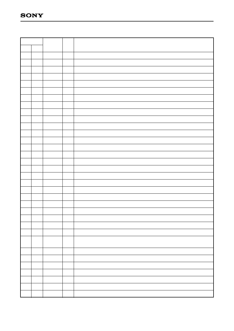
Pin Description
Pin No.
R
Q
79
80
1
2
3
4
5
6
7
8
9
10
11
12
13
14
15
16
17
18
19
20
21
22
23
24
25
26
27
28
29
30
31
32
1
2
3
4
5
6
7
8
9
10
11
12
13
14
15
16
17
18
19
20
21
22
23
24
25
26
27
28
29
30
31
32
33
34
SCOR
SBSO
EXCK
SQSO
SQCK
MUTE
SENS
XRST
DATA
XLAT
CLOK
V
SS
SEIN
CNIN
DATO
XLTO
CLKO
SPOA
SPOB
SPOC
XTSL
XLON
FOK
MON
MDP
MDS
LOCK
TEST
FILO
FILI
PCO
V
DD
AV
SS
1
CLTV
O
O
I
O
I
I
O
I
I
I
I
I
I
O
O
O
I
I
I
I
O
I
O
O
O
O
I
O
I
O
I
Outputs a high signal when either subcode sync S0 or S1 is detected.
Sub P to W serial output.
SBSO readout clock input.
Sub Q 80-bit serial output.
SQSO readout clock input.
High: mute; low: release
SENS output to CPU.
System reset. Reset when low.
Serial data input from CPU.
Latch input from CPU. Serial data is latched at the falling edge.
Serial data transfer clock input from CPU.
GND.
Sense input from SSP.
Track jump count signal input.
Serial data output to SSP.
Serial data latch output to SSP. Latched at the falling edge.
Serial data transfer clock output to SSP.
Microcomputer extended interface (input A).
Microcomputer extended interface (input B).
Microcomputer extended interface (input C).
Crystal selection input. Low for 16.9344MHz; high for 33.8688MHz
Microcomputer extended interface (output).
Focus OK input. Used for SENS output and the servo auto sequencer.
Spindle motor on/off control output.
Spindle motor servo control.
Spindle motor servo control.
GFS is sampled at 460Hz; when GFS is high, this pin outputs a high signal.
If GFS is low eight consecutive samples, this pin outputs low.
TEST pin. Normally GND.
Master PLL (slave = digital PLL) filter output.
Master PLL filter input.
Master PLL charge pump output.
Digital power supply for DSP.
Analog GND for DSP.
Master PLL VCO control voltage input.
Symbol
I/O
Description
≠ 5 ≠
CXD2508AQ/AR
Pin No.
R
Q
33
34
35
36
37
38
39
40
41
42
43
44
45
46
47
48
49
50
51
52
53
54
55
56
57
58
59
60
61
62
63
64
65
66
35
36
37
38
39
40
41
42
43
44
45
46
47
48
49
50
51
52
53
54
55
56
57
58
59
60
61
62
63
64
65
66
67
68
AV
DD1
RF
BIAS
ASYI
ASYO
ASYE
WDCK
LRCK
LRCKI
PCMD
PCMDI
BCK
BCKI
GTOP
XUGF
XPCK
GFS
RFCK
V
SS
C2PO
XROF
MNT3
MNT1
MNT0
FSTT
C4M
DOUT
EMPH
EMPHI
WFCK
ZEROL
ZEROR
DTS1
V
DD
I
I
I
O
I
O
O
I
O
I
O
I
O
O
O
O
O
O
O
O
O
O
O
O
O
O
I
O
O
O
I
Analog power supply for DSP.
EFM signal input.
Constant current input of asymmetry compensation circuit.
Comparator voltage input of asymmetry compensation circuit.
EFM full-swing output (low = Vss, high = V
DD
).
Low: asymmetry compensation off; high: asymmetry compensation on.
D/A interface for 48-bit slot. Word clock (2Fs).
D/A interface for 48-bit slot. LR clock (Fs).
LR clock input for DAC. (48-bit slot)
D/A interface. Serial data (two's complement, MSB first).
Audio data input for DAC. (48-bit slot)
D/A interface. Bit clock.
Bit clock input for DAC. (48-bit slot)
GTOP output.
XUGF output.
XPLCK output.
GFS output.
RFCK output.
GND.
C2PO output.
XRAOF output.
MNT3 output.
MNT1 output.
MNT0 output.
2/3 frequency-divider output for Pins 73 and 74.
4.2336MHz output.
Digital Out output.
Outputs high signal when the playback disc has emphasis, low signal when no
emphasis.
DAC de-emphasis on/off. High: on; low: off.
WFCK (write frame clock) output.
No-sound data detection output; high when no sound data is detected.
(Left channel)
No-sound data detection output; high when no sound data is detected.
(Right channel)
Test pin 1 for DAC; normally low.
Digital power supply for DAC.
Symbol
I/O
Description