 | –≠–ª–µ–∫—Ç—Ä–æ–Ω–Ω—ã–π –∫–æ–º–ø–æ–Ω–µ–Ω—Ç: CXD2719Q | –°–∫–∞—á–∞—Ç—å:  PDF PDF  ZIP ZIP |
Single-Chip Dolby Pro Logic Surround Decoder
Description
The CXD2719Q is a CMOS LSI developed for
Dolby Pro Logic Surround. A SRAM for short delay
and AD/DA converters are built in, and all functions
necessary for Dolby Pro Logic Surround such as an
adaptive matrix, a passive decoder including BNR,
auto input balance, a noise sequencer and center
channel mode control are contained on a single
chip.
Features
∑ Dolby Pro Logic Surround decoding with a single
chip
∑ 2-channel 1-bit AD converter, decimation filter and
prefilter operational amplifier
∑ 4-channel 1-bit DA converter, oversampling filter
and post filter
∑ Analog switch for DSP bypass
∑ Analog electronic attenuator (+1.5 to ≠29.5dB) for
center/surround channel trim
∑ 24K-bit SRAM for short delay
∑ No separation or other variance for digital
processing
∑ External parts reduced by incorporating analog
circuits
Functions
∑ Adaptive matrix
∑ Center channel mode control
(Normal/Phantom/Wide)
∑ Dolby 3 Stereo
∑ Auto input balance control (ON/OFF)
∑ Noise sequencer
∑ Variable delay time (0 to 34.8ms)
∑ 7 kHz low-pass filter (12dB/Oct)
∑ Modified Dolby B-type NR
∑ Simple SFC function
∑ SFC mode
∑ DSP bypass mode (L, R-channel through)
Structure
Silicon gate CMOS
Applications
Equipment having Dolby Pro Logic Surround
function such as AV amplifiers, receivers and
compact music systems
Absolute Maximum Ratings (Ta = 25∞C, V
SS
= 0V)
∑ Supply voltage
V
DD
V
SS
≠ 0.5 to +7.0
V
∑ Input voltage
V
I
V
SS
≠ 0.5 to V
DD
+ 0.5
V
∑ Output voltage
V
O
V
SS
≠ 0.5 to V
DD
+ 0.5
V
∑ Operating temperature
Topr
≠20 to +70
∞C
∑ Storage temperature
Tstg
≠55 to +150
∞C
Recommended Operating Conditions
∑ Supply voltage
V
DD
Analog system
4.75 to 5.25 (5.0 typ.)
V
Digital system
4.50 to 5.25 (5.0 typ.)
V
∑ Operating temperature
Ta
≠20 to +70
∞C
Input/Output Capacitance
∑ Input capacitance C
IN
9 (max.)
pF
∑ Output capacitance C
OUT
11 (max.)
pF
∑ Input/output capacitance
C
I/O
11 (max.)
pF
Measurement conditions: V
DD
= V
I
= 0V, F = 1MHz
Maximum Current Consumption
(Ta = 25∞C, V
DD
= 5.25V)
∑ Digital/analog block total: 166.7mA
Dolby level
∑ During analog input: 200 to 300mVrms
∑ During digital input: ≠20dBFS
Analog characteristics
Pro Logic ON: Dolby level = 300mVrms
Prefilter gain = ≠3.52dB
∑ S/N: L, Rch = 80dB, C, Sch = 72dB
∑ THD + N: L, Rch = 0.015%, C, Sch = 0.03%
All values for typ.
≠ 1 ≠
E98944-PS
Sony reserves the right to change products and specifications without prior notice. This information does not convey any license by
any implication or otherwise under any patents or other right. Application circuits shown, if any, are typical examples illustrating the
operation of the devices. Sony cannot assume responsibility for any problems arising out of the use of these circuits.
CXD2719Q
80 pin QFP (Plastic)
This device is available only to parties obtaining the license from Dolby Laboratories Licensing Corporation.
"Dolby", the double-D symbol and "Pro Logic" are trademarks of Dolby Laboratories Licensing Corporation.
≠ 2 ≠
CXD2719Q
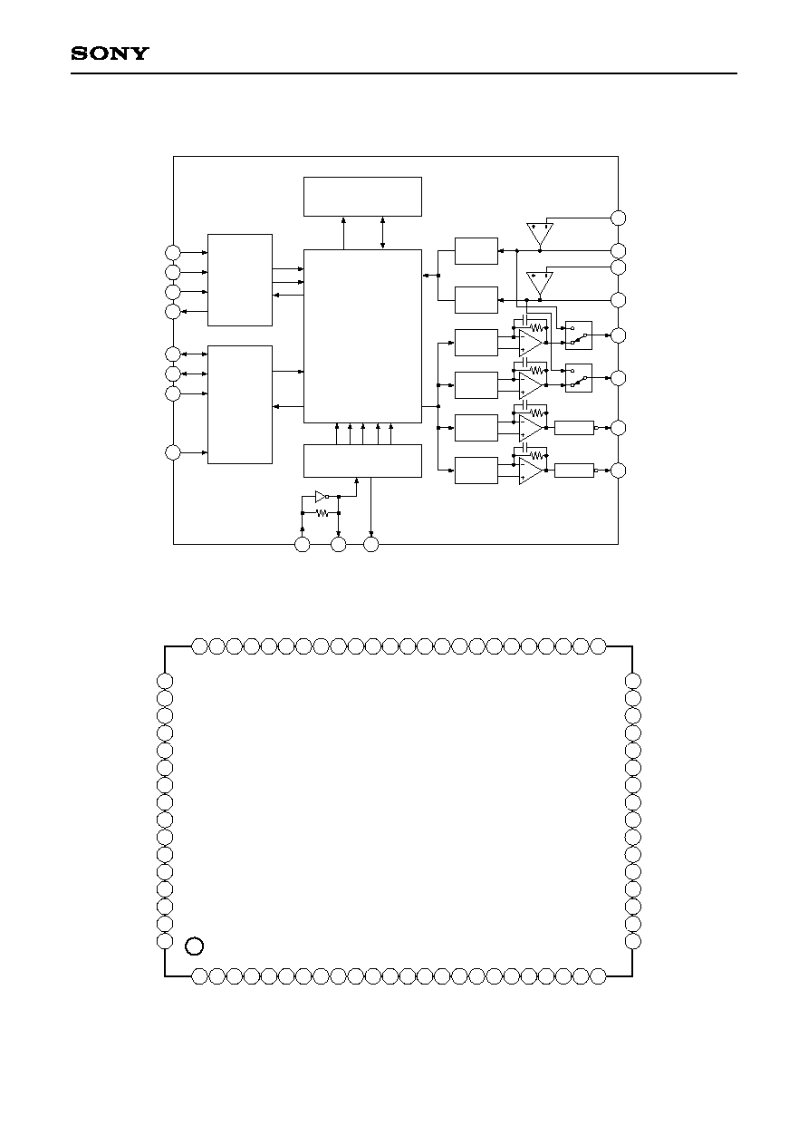
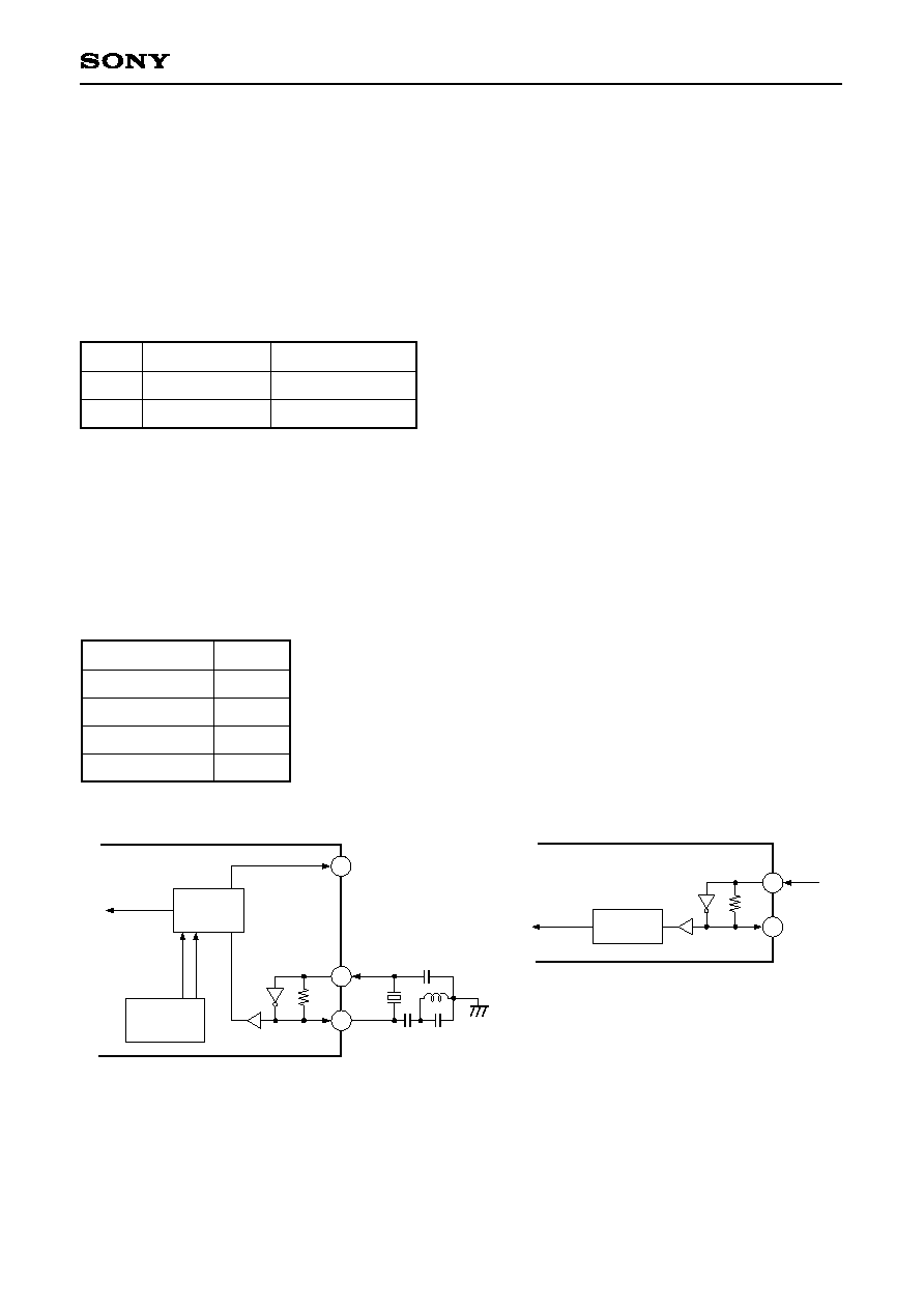
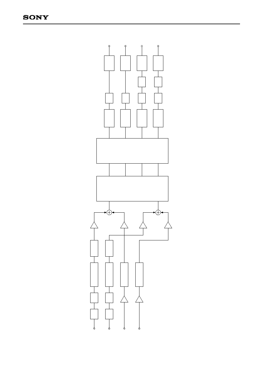
Block Diagram
XSOUT
XCOUT
ROUT
LOUT
LO2
RIN
LO1
LIN
17
23
30
35
32
42
57
58
DAC1
DAC2
DAC3
DAC4
Trim Vol
Trim Vol
ADC2
ADC1
Analog SW
Analog SW
DSP
24K bit DELAY RAM
CLOCK GENERATOR
/TIMING CIRCUIT
MICRO-
COMPUTER
I/F
SERIAL
DATA
I/F
26
27
39
38
55
60
46
47
49
50
33
X
T
L
I
X
T
L
O
B
F
O
T
XMST
SI
BCK
REDY
XLAT
SCK
RVDT
LRCK
(Phase Inverted Output)
(Phase Inverted Output)
Pin Configuration
T
.
P
T
.
P
T
.
P
T
.
P
V
S
S
0
T
.
P
T
.
P
T
.
P
T
S
T
0
V
D
D
0
V
S
S
1
T
S
T
1
T
S
T
2
T
S
T
3
T
S
T
4
X
R
S
T
B
F
O
T
C
S
L
1
C
S
L
2
V
S
S
2
A
V
S
3
A
V
D
3
L
O
U
T
A
V
D
1
V
S
S
6
T
.
P
T
.
P
T
.
P
B
C
K
T
.
P
S
I
T
.
P
V
S
S
4
V
D
D
1
X
S
2
4
R
V
D
T
T
.
P
R
E
D
Y
S
C
K
V
S
S
3
A
V
S
4
A
V
D
4
R
O
U
T
A
V
D
2
AVS1
LO1
LIN
AVD5
AVS5
XCOUT
AVDX
XTLO
XTLI
AVSX
XSOUT
AVS6
AVD6
RIN
LO2
AVS2
X
L
A
T
V
S
S
5
L
R
C
K
X
M
S
T
1
4
5
6
7
8
9 10
2
3
11 12 13 14 15 16 17 18 19 20 21 22 23 24
25
26
27
28
29
30
31
32
33
34
35
36
37
38
39
40
41
42
43
44
45
46
47
48
49
50
51
52
53
54
55
56
57
58
59
60
61
63
64
62
65
66
67
68
69
70
71
72
73
74
75
76
77
78
79
80
T.P
T.P
T.P
T.P
T.P
T.P
V
SS
7
V
DD
2
T.P
T.P
T.P
T.P
T.P
T.P
T.P
T.P
≠ 3 ≠
CXD2719Q
Pin Description
Notations in parentheses indicate the fixed pin connection status.
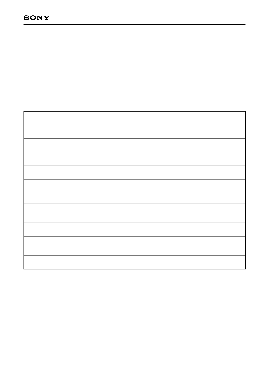
1 to 3
4
5 to 8
9
10
11
12
13
14
15
16
17
18
19
20
21
22
23
24
25
26
27
28
29
30
31
32
33
34
35
36
37
T.P
V
SS
0
T.P
TST0
V
DD
0
V
SS
1
TST1
TST2
TST3
TST4
XRST
BFOT
CSL1
CSL2
V
SS
2
AVS3
AVD3
LOUT
AVD1
AVS1
LO1
LIN
AVD5
AVS5
XCOUT
AVDX
XTLO
XTLI
AVSX
XSOUT
AVS6
AVD6
O
--
O
I
--
--
I
I
I
I
I
O
I
I
--
--
--
O
--
--
O
I
--
--
O
--
O
I
--
O
--
--
Test monitor. Normally outputs Low.
(OPEN)
Digital GND.
(V
SS
)
Test monitor. Normally outputs Low.
(OPEN)
Test. Normally fixed Low.
(V
SS
)
Digital power supply.
(V
DD
)
Digital GND.
(V
SS
)
Test. Normally fixed Low.
(V
SS
)
Test. Normally fixed Low.
(V
SS
)
Test. Normally fixed Low.
(V
SS
)
Test. Normally fixed Low.
(V
SS
)
System reset input. Reset when Low.
Clock, frequency-division output. [384/768/256/512fs]
Test. Normally fixed High.
(V
DD
)
Test. Normally fixed Low.
(V
SS
)
Digital GND.
(V
SS
)
L-ch DA converter GND.
(AV
SS
)
L-ch DA converter power supply.
(AV
DD
)
L-ch DA converter output.
L-ch AD converter power supply.
(AV
DD
)
L-ch AD converter GND.
(AV
SS
)
L-ch AD converter LPF operational amplifier inverted output.
L-ch AD converter analog input.
C-ch DA converter power supply.
(AV
DD
)
C-ch DA converter GND.
(AV
SS
)
C-ch DA converter output.
Analog power supply for master clock.
(AV
DD
)
Crystal oscillator circuit output.
Crystal oscillator circuit input.
Analog GND for master clock.
(AV
SS
)
S-ch DA converter output.
S-ch DA converter GND.
(AV
SS
)
S-ch DA converter power supply.
(AV
DD
)
Pin No.
Symbol
I/O
Description
(OPEN): Open, (V
DD
): +5V digital power supply, (AV
DD
): +5V analog power supply,
(V
SS
): Digital GND, (AV
SS
): Analog GND
≠ 4 ≠
CXD2719Q
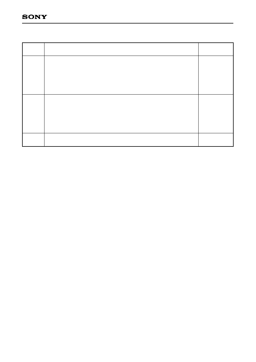
Notations in parentheses indicate the fixed pin connection status.
(OPEN): Open, (V
DD
): +5V digital power supply, (AV
DD
): +5V analog power supply,
(V
SS
): Digital GND, (AV
SS
): Analog GND
There are three digital and seven analog power supplies, but the power-on sequence is not specified.
Pin No.
38
39
40
41
42
43
44
45
46
47
48
49
50
51
52
53
54
55
56
57
58
59
60
61 to 63
64
65 to 72
73
74
75 to 80
Symbol
RIN
LO2
AVS2
AVD2
ROUT
AVD4
AVS4
V
SS
3
SCK
REDY
T.P
XLAT
RVDT
XS24
V
DD
1
V
SS
4
T.P
SI
T.P
BCK
LRCK
V
SS
5
XMST
T.P
V
SS
6
T.P
V
DD
2
V
SS
7
T.P
I/O
I
O
--
--
O
--
--
--
I
O
O
I
I
I
--
--
O
I
I
I/O
I/O
--
I
O
--
O
--
--
O
Description
R-ch AD converter analog input.
R-ch AD converter LPF operational amplifier inverted output.
R-ch AD converter GND.
(AV
SS
)
R-ch AD converter power supply.
(AV
DD
)
R-ch DA converter output.
R-ch DA converter power supply. (AV
DD
)
R-ch DA converter GND.
(AV
SS
)
Digital GND.
(V
SS
)
Shift clock input for microcomputer interface.
Transfer enabling signal output for microcomputer interface. Transfer prohibited when Low.
Test monitor. Normally outputs Hi-Z.
(OPEN)
Latch input for microcomputer interface.
Data input for microcomputer interface.
Serial data 24-/32-bit slot selection. 24-bit slot when Low. (valid for slave mode)
Digital power supply.
(V
DD
)
Digital GND.
(V
SS
)
Test monitor. Normally outputs Low.
(OPEN)
1-sampling 2-channel serial data input.
Test input. Normally inputs Low.
(V
SS
)
Serial bit transfer clock for serial I/O data SI and SO.
Sampling frequency clock for serial I/O data SI and SO.
Digital GND.
(V
SS
)
BCK, LRCK master/slave mode switching input. Master mode when Low.
Test monitor. Normally outputs Low.
(OPEN)
Digital GND.
(V
SS
)
Test monitor. Normally outputs Low.
(OPEN)
Digital power supply.
(V
DD
)
Digital GND.
(V
SS
)
Test monitor. Normally outputs Low.
(OPEN)
≠ 5 ≠
CXD2719Q
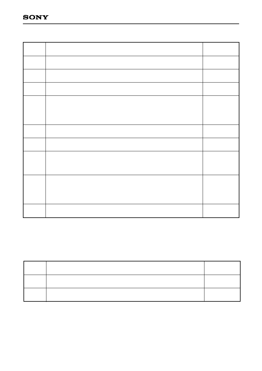
DC Characteristics
(AVD1 to 6 = AVDX = V
DD
0 to 2 = 5V ± 5%, AVS1 to 6 = AVSX = V
SS
0 to 7 = 0V, Ta = ≠20 to +70∞C)
Item
Symbol
Conditions
Min.
Max.
Unit
Applicable pins
Typ.
V
V
V
V
V
V
V
V
V
V
V
µA
µA
µA
1
,
2
,
7
1
,
2
,
7
5
5
3
,
6
3
,
6
4
8
,
9
8
,
9
,
10
11
11
1
,
5
,
7
2
,
3
,
6
9
,
10
Resistance between
7
and
11
High level
Low level
High level
Low level
High level
Low level
High level
Low level
High level
Low level
Input voltage
(1)
Input voltage
(2)
Input voltage
(3)
Input voltage (4)
Output voltage
(1)
Output voltage
(2)
Input leak current (1)
Input leak current (2)
Output leak current
Feedback resistance
V
IH
V
IL
V
IH
V
IL
V
IH
V
IL
V
IN
V
OH
V
OL
V
OH
V
OL
I
I
I
I
I
OZ
R
FB
CMOS input
Schmitt input
TTL input
Analog input
I
OH
= ≠2.0mA
I
OL
= 4.0mA
I
OH
= ≠12.0mA
I
OL
= 12.0mA
V
IH
= V
DD
, V
SS
V
IH
= V
DD
, V
SS
V
IH
= V
DD
, V
SS
0.7V
DD
0.8V
DD
2.2
V
SS
V
DD
≠ 0.8
V
DD
/2
≠10
≠40
≠40
250k
1M
0.3V
DD
0.2V
DD
0.8
V
DD
0.4
V
DD
/2
10
40
40
2.5M
1
CSL2, CSL1, TST0 to TST4, XMST
2
XLAT, RVDT, XS24, SCK
3
SI
4
LIN, RIN
5
XRST
6
During input to bidirectional pins BCK, LRCK
7
XTLI
8
During output from bidirectional pins BCK, LRCK
9
BFOT
10
REDY
11
XTLO
≠ 6 ≠
CXD2719Q
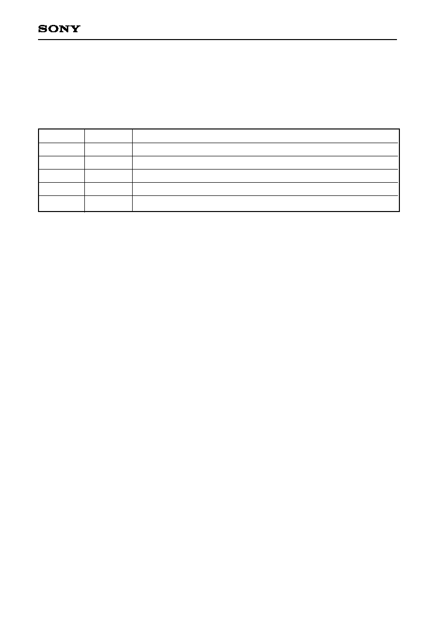
AC Characteristics
(AVD1 to 6 = AVDX = V
DD
0 to 2 = 5V ± 5%, AVS1 to 6 = AVDX = V
SS
0 to 7 = 0V, Ta = ≠20 to +70∞C)
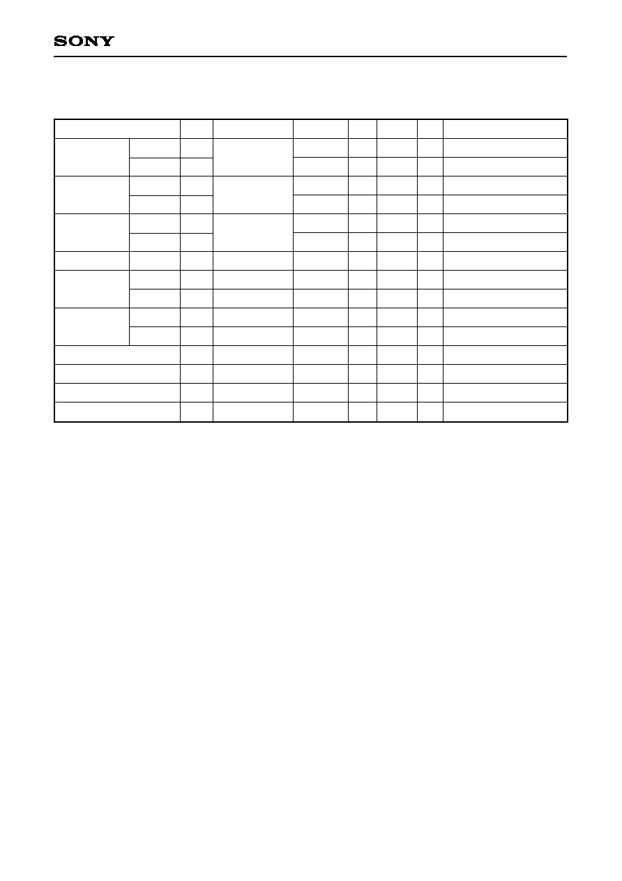
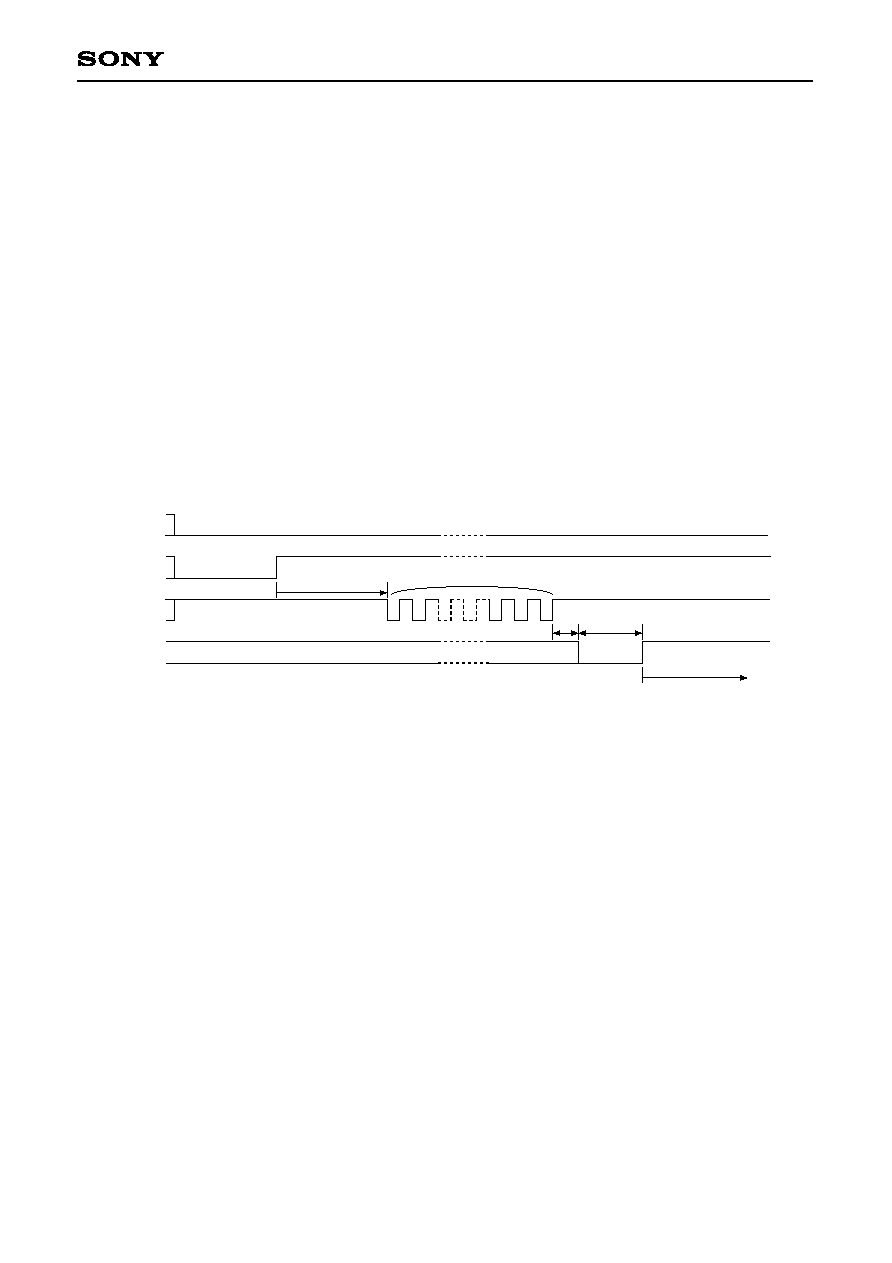
Input Timing from Power-on to Input Pin
∑∑∑∑∑
V
DD
XTLI
XRST
Input pins
0.7V
DD
0.3V
DD
1/fs or more
1/fs or more
Determined by the crystal and other external circuit conditions
Stable (clock applied correctly)
0.8V
DD
0.2V
DD
0.95V
DD
First input
BCK
SI
LRCK
tHLR
tSLR
0.7V
DD
0.3V
DD
0.7V
DD
0.3V
DD
tSSI
tHSI
0.7V
DD
0.3V
DD
BCK
LRCK
tDLR
Serial Audio Interface Timing
[Slave mode]
[Master mode]
Item
SI setup time
SI hold time
LRCK setup time
LRCK hold time
LRCK delay time
Symbol
t
SSI
t
HSI
t
SLR
t
HLR
t
DLR
Conditions
Slave mode
Slave mode
Slave mode
Slave mode
Master mode, C
L
= 120pF
Min.
20
40
20
40
Max.
50
Unit
ns
ns
ns
ns
ns
≠ 7 ≠
CXD2719Q
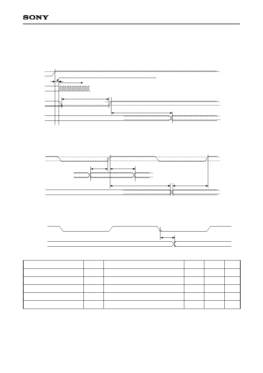
Microcomputer Interface Timing
Transfer timing for address section, transfer mode section and data section LSB
Transfer timing from data section MSB to address section and transfer mode section
Notes) 1. t is the cycle of 2/3 the clock frequency applied to the XTLI pin. (512fs)
2. The REDY pin is the value for C
L
= 60pF.
Item
RVDT data setup time relative to SCK rise
RVDT data hold time from SCK rise
SCK Low level width
SCK High level width
XLAT Low level width
XLAT High level width
SCK rise preceding time relative to XLAT rise
SCK rise wait time relative to XLAT rise
Delay time to REDY fall relative to SCK rise
REDY fall preceding time relative to SCK rise
REDY rise preceding time relative to XLAT rise
REDY rise preceding time relative to SCK fall
XLAT fall wait time relative to SCK rise
XLAT fall delay time relative to REDY fall
SCK rise wait time for next transfer
Symbol
tDS
tDH
tSWL
tSWH
tLWL
tLWH
tSLP
tLSD
tSBD
tBSP
tRLP
tRSDP
tSLD
tLDR
tSS
Min.
20
1t + 20
1t + 20
1t + 20
1t + 20
1t + 20
20
3t + 20
20
20
20
3t + 20
20
2t + 40
Max.
4t + 50
Unit
ns
ns
ns
ns
ns
ns
ns
ns
ns
ns
ns
ns
ns
ns
ns
RVDT
SCK
tSWL
tSWH
tDS
tDH
Address LSB
Mode MSB
0.3V
DD
0.7V
DD
0.3V
DD
0.7V
DD
tSLP
tLSD
tLWL
0.3V
DD
0.7V
DD
XLAT
REDY
Data LSB
Data MSB
RVDT
SCK
XLAT
REDY
Mode MSB
0.3V
DD
0.7V
DD
Address LSB
Data MSB
tSS
tLDR
tSBD
tSLD
tBSP
0.3V
DD
0.7V
DD
tRLP
0.3V
DD
0.7V
DD
≠ 8 ≠
CXD2719Q
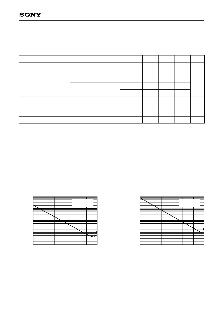
Analog Characteristics
(AVD0 to 6 = V
DD
0 to 2 = AVDX = 5.0V, AVS0 to 6 = V
SS
0 to 7 = AVSX = 0.0V, fs = 44.1kHz, Ta = 25∞C)
When Pro Logic mode is on, the input signal level while measuring the center (C) and surround (S) channels
should be ≠3dB smaller than the input level while measuring the left (L) and right (R) channels. Note that the C
channel is input in-phase to the L channel, and the S channel is input at reversed phase to the R channel.
The input level is the same for all measurement items when Pro Logic mode is off.
1. ADC + DAC Connection Total Characteristics
In addition to the ADC and DAC, the total characteristics include the prefilter with built-in operational amplifier,
built-in post filter, and trim volume. Use the analog I/O circuits in the Application Circuit for the measurement
circuit.
1-1. When Pro Logic mode is on
Unless otherwise specified, the measurement conditions are as given below.
∑ V
IN
(L, R) = 300mVrms, V
IN
(C, S) = 212mVrms (= 0dB)
∑ f
IN
= 1kHz
1
When V
IN
= 200mVrms (= ≠3.52dB), the S/N ratio is 3.52dB smaller than the values noted in the table above.
2
V
IN
(L, R) = 2.0Vrms, V
IN
(C, S) = 1.414Vrms
3
V
IN
(L, R) = 300mVrms, V
IN
(C, S) = 212mVrms
4
V
IN
(L, R) = 200mVrms, V
IN
(C, S) = 141mVrms
5
When the L and R channel gain deviation is 0.1dB or less for the ADC front-end prefilter output.
6
Includes the amplification (L/Rch...5.27dB, C/Sch...13.72dB) of the external amplifier.
7
The trim volume is set to 0dB.
L, R
C, S
L, R
C
S
L, R
C, S
L, R
C, S
L, R
C, S
L, R
C
S
L, R
C, S
(all)
(all)
L, R
C, S
7
70
65
25
25
250
80
72
60
56
64
0.04
0.007
0.015
0.03
0.02
0.04
0.12
0.18
0.04
16.5
60
40
280
±0.2
36
91
3.9
≠13.2
1.00
1.00
310
dB
%
dB
dB
Vrms
dB
mA
dB
S/N ratio
1
THD + N
Head room
Matrix rejection
Output level
Level difference between channels
Current consumption
Power supply rejection
ratio
6
CCIR/ARM filter
10Hz to 500kHz
10Hz to 20kHz
V
IN
= 16.5dB
2
10Hz to 20kHz
V
IN
= 0dB
3
10Hz to 20kHz
V
IN
= ≠3.52dB
4
10Hz to 500kHz
10Hz to 20kHz, THD + N = 1%
5
Analog system (including oscillator circuit)
Digital system
1mVrms, 100Hz sine wave
Channels
Min.
Typ.
Max.
Unit
Item
Measurement conditions
≠ 9 ≠
CXD2719Q
1-2. When Pro Logic mode is off
Unless otherwise specified, the measurement conditions are as given below.
∑ V
IN
(L, R, C, S) = 2.0Vrms (= 0dB)
∑ f
IN
= 1kHz
L, R
C, S
(all)
L, R
C, S
L, R
C, S
(all)
(all)
1.7
97
90
0.03
0.004
0.01
93
83
1.33
1.85
1.00
2.0
dB
%
dB
Vrms
Vrms
S/N ratio
THD + N
11
Dynamic range
12
ADC maximum input level
13
Output level
14
EIAJ
(with "A" weighting filter)
EIAJ (0dB)
EIAJ (≠3dB)
EIAJ (≠60dB)
(Full-scale output)
11
See Graphs 1a and 1b.
12
THD + N during ≠60 dB input
13
The analog input level at which the ADC outputs full scale varies according to supply voltage AVDn.
When supply voltage AVDn contains deviation, calculate the maximum input level from (Formula 1) below
and adjust the level with the ADC front-end prefilter, etc., so that the waveform is not clipped at the
minimum voltage.
ADC maximum input level [Vrms] = 1.33 [Vrms]
◊
(Formula 1)
14
Like the ADC, the DAC conversion gain also varies according to supply voltage AVDn. However, the DAC
has the reverse characteristics of the ADC, so the total gain between the ADC and DAC is constant.
Minimum supply voltage [V]
5.0 [V]
≠60
≠50
≠40
≠30
≠20
≠10
0
0.001
0.01
0.1
1
10
Graph 1a. L, R Channel Characteristics
Analog input level [dB]
T
H
D
+
N
[
%
]
0dB = 2Vrms
fin = 1kHz
≠60
≠50
≠40
≠30
≠20
≠10
0
0.001
0.01
0.1
1
10
Graph 1b. C, S Channel Characteristics
Analog input level [dB]
T
H
D
+
N
[
%
]
0dB = 2Vrms
fin = 1kHz
Channels
Min.
Typ.
Max.
Unit
Item
Measurement conditions
≠ 10 ≠
CXD2719Q
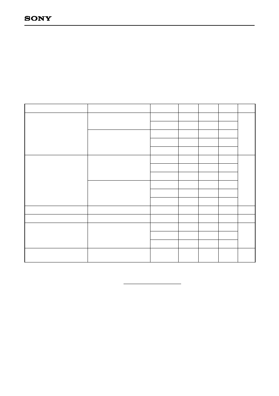
2. DAC Characteristics
In addition to the DAC, these characteristics include the built-in post filter and trim volume. Use the digital input
and analog output circuits in the Application Circuit for the measurement circuit.
2-1. When Pro Logic mode is on
Unless otherwise specified, the measurement conditions are as given below.
∑ Digital data = ≠20dBFS
∑ f
IN
= 3kHz
Channels
L, R
C, S
L, R
C
S
L, R
C
S
L, R
C
S
L, R-in
C-in
S-in
(all)
Min.
Typ.
77
68
60
52
65
0.05
0.08
0.06
0.15
0.3
0.08
≠20
200
62
87
79
±0.2
Max.
Unit
dB
%
dBFS
mVrms
dB
dB
Item
S/N ratio
THD + N
Dolby level
Output level
31
Matrix rejection
Level difference between
channels
Measurement conditions
CCIR/ARM filter
Data = ≠20dBFS
10Hz to 500kHz
Data = ≠20dBFS
10Hz to 20kHz
Data = ≠20dBFS
10Hz to 500kHz
Data = ≠20dBFS
Data = ≠20dBFS
f
IN
= 3kHz
31
The output level depends on supply voltage AVDn as shown in (Formula 2) below.
Output level [mVrms] = 285 [mVrms]
◊
(Formula 2)
Supply voltage AVDn [V]
5.0 [V]
≠ 11 ≠
CXD2719Q
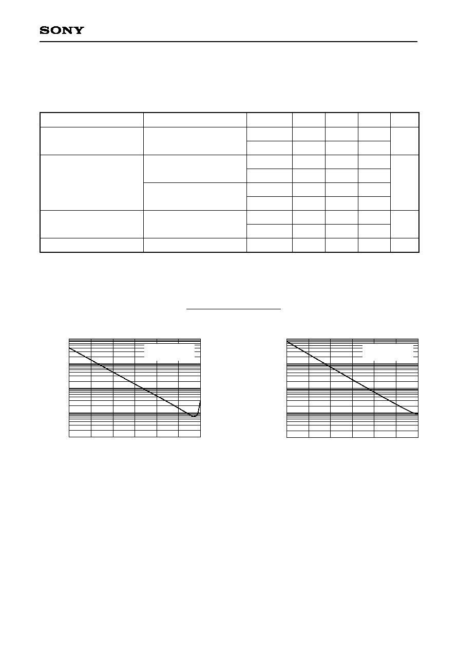
2-2. When Pro Logic mode is off
Unless otherwise specified, the measurement conditions are as given below.
∑ Digital data = Full scale (0dBFS)
∑ f
IN
= 1kHz
Channels
L, R
C, S
L, R
C, S
L, R
C, S
L, R
C, S
(all)
Min.
Typ.
100
91
0.03
0.007
0.007
0.01
87
83
2.0
Max.
Unit
dB
%
dB
Vrms
Item
S/N ratio
THD + N
41
Dynamic range
42
Output level
43
Measurement conditions
EIAJ
(with "A" weighting filter)
EIAJ (0dB)
EIAJ (≠3dB)
EIAJ (≠60dB)
41
See Graphs 2a and 2b.
42
THD + N during ≠60dB input
43
The output level depends on supply voltage AVDn as shown in (Formula 3) below.
Output level [Vrms] = 1.9 [Vrms]
◊
(Formula 3)
Supply voltage AVDn [V]
5.0 [V]
≠60
≠50
≠40
≠30
≠20
≠10
0
0.001
0.01
0.1
1
10
Graph 2b. C, S Channel Characteristics
Digital input level [dB]
T
H
D
+
N
[
%
]
0dB = Full scale
fin = 1kHz
≠60
≠50
≠40
≠30
≠20
≠10
0
0.001
0.01
0.1
1
10
Graph 2a. L, R Channel Characteristics
T
H
D
+
N
[
%
]
Digital input level [dB]
0dB = Full scale
fin = 1kHz
≠ 12 ≠
CXD2719Q
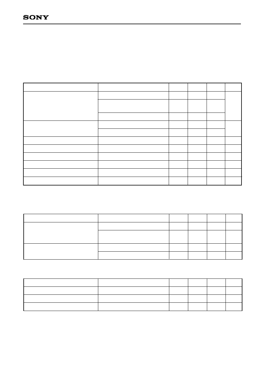
3. Bypass Mode Characteristics (L, R channels only)
These are the characteristics without passing through the DSP, and including the prefilter with built-in
operational amplifier and the built-in post filter. Use the analog I/O circuits in the Application Circuit for the
measurement circuit. Unless otherwise specified, the measurement conditions are as given below.
∑ f
IN
= 1kHz
∑ V
IN
(L, R) = 2.0Vrms (= 0dB)
Min.
Typ.
97
100
80
0.008
0.005
95
2.5
2.0
±0.2
105
7.5
Max.
Unit
dB
%
dB
Vrms
Vrms
dB
dB
dB
Item
S/N ratio
THD + N
Dynamic range
51
Maximum input level
Output level
Level difference between channels
Channel separation
Power supply rejection ratio
52
Measurement conditions
CCIR/ARM filter
10Hz to 20kHz, "A" weighting filter
10Hz to 500kHz
10Hz to 500kHz
10Hz to 20kHz
10Hz to 20kHz, V
IN
= ≠60dB
THD + N = 0.05%
1mVrms, 100Hz sine wave
Min.
10
10
Typ.
104
Max.
20
Unit
k
dB
k
kHz
Item
Prefilter
Post filter
Measurement conditions
Feedback resistance value
Maximum amplification rate
(100kHz or less)
Load resistance value
Cut-off frequency (= fc)
Min.
Typ.
1.5
≠29.5
1.0
Max.
Unit
dB
dB
dB
Item
Maximum gain
Minimum gain
Variable step
Symbol
TRIMmax
TRIMmin
TRIMstep
51
THD + N during ≠60dB input
52
Includes the amplification (5.27dB) of the external amplifier.
4. Filter Characteristics
5. Trim Volume Characteristics
≠ 13 ≠
CXD2719Q
Description of Functions
1. Master/Slave Modes
[Relevant pins] XMST, LRCK, BCK
When using the CXD2719Q alone without digital input, set the CXD2719Q to master mode.
When using digital input, the CXD2719Q may be set to either master mode or slave mode.
The clock applied to LRCK and BCK in slave mode must be synchronized to either the crystal oscillator clock
of the XTLI and XTLO pins or the external clock input from the XTLI pin.
Table 1-1. LRCK, BCK Mode Setting
XMST
H
L
Mode
Slave mode
Master mode
LRCK, BCK I/O
Input
Output
SQC05
0
0
1
1
SQC04
0
1
0
1
BFOT
384fs
256fs
512fs
768fs
2. Master Clock System
[Relevant pins] XTLI, XTLO, BFOT
768fs (fs = 32 to 44.1kHz) is assumed for the master clock system, and the connection is as shown below.
BFOT outputs the clock obtained by frequency dividing the master clock. The frequency division ratio can be
changed by the setup register (SQC04, SQC05). (See "6. Setup Register".)
(1) Master
(2) Slave
O
I
O
Frequency
divider
Setup
Register
512fs
XTLI
XTLO
768fs
BFOT
256fs/384fs/512fs/768fs
O
512fs
XTLI
XTLO
768fs
I
OPEN
Frequency
divider
Fig. 2-1.
Note) Oscillation circuits may differ according to peripheral circuit and
substrate. Consult with crystal oscillator manufacturers about the
selecting oscillation circuits.
≠ 14 ≠
CXD2719Q
3. Reset Circuit
[Relevant pins] XRST, XTLI, XTLO
This LSI must be reset after the power is turned on.
Reset is done by setting the XRST pin Low for 1/fs or more after the supply voltage satisfies the recommended
operating condition, and the crystal oscillator clock of the XTLI and XTLO pins or the external clock input from
the XTLI pin is correctly applied. (See "AC Characteristics".)
4. Serial Audio Interface (SIF)
[Relevant pins] SI, BCK, LRCK, XS24, XMST
Serial data is used for the external communication of the digital audio data. The CXD2719Q has only one input
system, and 2 channels of data are input each sampling cycle. Either the 32-bit clock mode or the 24-bit clock
mode can be selected. In master mode, the mode is fixed to the 32-bit clock mode.
(1) Pin Configuration (The pins shown in the table below are assigned to the SIF.)
Serial input; taken with synchronized to BCK.
BCK I/O; either 32-bit clock mode (64fs) or 24-bit clock mode (48fs). BCK output supports
32-bit clock mode only.
LRCK I/O (1fs).
SIO slot number (24/32) selection input. Low: 24-bit slot; High: 32-bit slot.
Valid only in slave mode. Set High in master mode.
Do not switch between High and Low during DSP operation.
BCK, LRCK master mode/slave mode switching input.
Low: master mode; High: slave mode.
Symbol
SI
BCK
LRCK
XS24
XMST
I/O
Function
I
I/O
I/O
I
I
"0": normal,
"1": IIS
"0": Lch "H", "1": Lch "L"
"0": edge
,
"1" : edge
Setup register
SQC15
SQC14
SQC13
Function
Contents
LRCK format
LRCK polarity selection
BCK polarity selection relative to LRCK edge
Valid only in slave mode. Fix to "0" in master
mode.
Table 4-1. Pin Configuration
Table 4-2. LRCK/BCK Mode Setting
(2) Operation Modes
The LRCK/BCK mode can be selected by the setup register settings as follows. (See "6. Setup Register".)
LRCK/BCK Mode Setting
≠ 15 ≠
CXD2719Q
Table 4-3. Setup Register Settings
(3) SIF Format
The serial audio interface has only one input system, and except for the slot number, the following formats can
be set by setting the setup register. The serial audio interface can also support IIS format to enable connection
to Philips and other company's devices.
The timing charts for each data format are given on the following page.
SQC12
0
0
1
1
SQC11
0
1
0
1
Data arrangement/Frontward or rearward truncation/Data word length
MSB first/Frontward truncation/24 bits
MSB first/Rearward truncation/16 bits
MSB first/Rearward truncation/18 bits
MSB first/Rearward truncation/20 bits
All formats support either the 24- or 32-bit slot in slave mode.
≠ 16 ≠
CXD2719Q
2
3
2
2
2
1
2
0
1
9
1
8
1
7
1
6
1
5
1
4
1
3
1
2
1
1
1
0
0
9
0
8
0
7
0
6
0
5
0
4
0
3
0
2
0
1
0
0
1
5
1
4
1
3
1
2
1
1
1
0
0
9
0
8
0
7
0
6
0
5
0
4
0
3
0
2
0
1
0
0
1
5
1
4
1
3
1
2
1
1
1
0
0
9
0
8
0
7
0
6
0
5
0
4
0
3
0
2
0
1
0
0
1
5
1
4
1
3
1
2
1
1
1
0
0
9
0
8
0
7
0
6
0
5
0
4
0
3
0
2
0
1
0
0
1
7
1
6
1
5
1
4
1
3
1
2
1
1
1
0
0
9
0
8
0
7
0
6
0
5
0
4
0
3
0
2
0
1
0
0
1
7
1
6
1
5
1
4
1
3
1
2
1
1
1
0
0
9
0
8
0
7
0
6
0
5
0
4
0
3
0
2
0
1
0
0
1
7
1
6
1
9
1
8
1
9
1
5
1
4
1
3
1
2
1
1
1
0
0
9
0
8
0
7
0
6
0
5
0
4
0
3
0
2
0
1
0
0
1
7
1
6
1
8
L
R
C
K
B
C
K
S
I
2
3
2
2
2
1
2
0
1
9
1
8
1
7
1
6
1
5
1
4
1
3
1
2
1
1
1
0
0
9
0
8
0
7
0
6
0
5
0
4
0
3
0
2
0
1
0
0
∑
M
S
B
f
i
r
s
t
2
4
b
i
t
s
f
r
o
n
t
w
a
r
d
t
r
u
n
c
a
t
i
o
n
(
S
Q
C
1
2
,
1
1
=
0
,
0
)
∑
M
S
B
f
i
r
s
t
1
6
b
i
t
s
r
e
a
r
w
a
r
d
t
r
u
n
c
a
t
i
o
n
(
S
Q
C
1
2
,
1
1
=
0
,
1
)
∑
M
S
B
f
i
r
s
t
1
8
b
i
t
s
r
e
a
r
w
a
r
d
t
r
u
n
c
a
t
i
o
n
(
S
Q
C
1
2
,
1
1
=
1
,
0
)
∑
M
S
B
f
i
r
s
t
2
0
b
i
t
s
r
e
a
r
w
a
r
d
t
r
u
n
c
a
t
i
o
n
(
S
Q
C
1
2
,
1
1
=
1
,
1
)
L
c
h
R
c
h
L
S
B
M
S
B
I
a
v
a
l
i
d
L
S
B
I
a
v
a
l
i
d
M
S
B
I
a
v
a
l
i
d
L
S
B
M
S
B
I
a
v
a
l
i
d
L
S
B
L
S
B
M
S
B
I
a
v
a
l
i
d
L
S
B
L
S
B
M
S
B
I
a
v
a
l
i
d
L
S
B
M
S
B
M
S
B
I
a
v
a
l
i
d
I
a
v
a
l
i
d
M
S
B
M
S
B
2
3
2
2
2
1
2
0
1
9
1
8
1
7
1
6
1
5
1
4
1
3
1
2
1
1
1
0
0
9
0
8
0
7
0
6
0
5
0
4
0
3
0
2
0
1
0
0
2
3
2
2
2
1
2
0
1
9
1
8
1
7
1
6
1
5
1
4
1
3
1
2
1
1
1
0
0
9
0
8
0
7
0
6
0
5
0
4
0
3
0
2
0
1
0
0
1
5
1
4
1
3
1
2
1
1
1
0
0
9
0
8
0
7
0
6
0
5
0
4
0
3
0
2
0
1
0
0
1
5
1
4
1
3
1
2
1
1
1
0
0
9
0
8
0
7
0
6
0
5
0
4
0
3
0
2
0
1
0
0
1
7
1
6
1
5
1
4
1
3
1
2
1
1
1
0
0
9
0
8
0
7
0
6
0
5
0
4
0
3
0
2
0
1
0
0
1
7
1
6
1
5
1
4
1
3
1
2
1
1
1
0
0
9
0
8
0
7
0
6
0
5
0
4
0
3
0
2
0
1
0
0
1
9
1
8
1
7
1
6
1
5
1
4
1
3
1
2
1
1
1
0
0
9
0
8
0
7
0
6
0
5
0
4
0
3
0
2
0
1
0
0
1
9
1
8
1
7
1
6
1
5
1
4
1
3
1
2
1
1
1
0
0
9
0
8
0
7
0
6
0
5
0
4
0
3
0
2
0
1
0
0
L
R
C
K
B
C
K
S
I
L
S
B
M
S
B
L
S
B
M
S
B
L
S
B
M
S
B
I
a
v
a
l
i
d
L
S
B
L
S
B
M
S
B
I
a
v
a
l
i
d
L
S
B
L
S
B
M
S
B
I
a
v
a
l
i
d
L
S
B
M
S
B
M
S
B
I
a
v
a
l
i
d
I
a
v
a
l
i
d
I
a
v
a
l
i
d
L
c
h
R
c
h
M
S
B
∑
M
S
B
f
i
r
s
t
2
4
b
i
t
s
(
S
Q
C
1
2
,
1
1
=
0
,
0
)
∑
M
S
B
f
i
r
s
t
1
6
b
i
t
s
r
e
a
r
w
a
r
d
t
r
u
n
c
a
t
i
o
n
(
S
Q
C
1
2
,
1
1
=
0
,
1
)
∑
M
S
B
f
i
r
s
t
1
8
b
i
t
s
r
e
a
r
w
a
r
d
t
r
u
n
c
a
t
i
o
n
(
S
Q
C
1
2
,
1
1
=
1
,
0
)
∑
M
S
B
f
i
r
s
t
2
0
b
i
t
s
r
e
a
r
w
a
r
d
t
r
u
n
c
a
t
i
o
n
(
S
Q
C
1
2
,
1
1
=
1
,
1
)
Digital Audio Data Input Timing
(with polarities: SQC15 = 0, SQC14 = 0, SQC13 = 0)
32-bit slot
24-bit slot
≠ 17 ≠
CXD2719Q
5. Microcomputer Interface
[Relevant pins] RVDT, SCK, XLAT, REDY
The CXD2719Q performs the serial audio interface format setting and the coefficient settings such as volume
and filter by serial data from the microcomputer.
(1) Pin Configuration
The four external pins indicated in the table below are assigned to the microcomputer interface.
Serial data input from microcomputer.
Shift clock for serial data. Input data from RVDT is taken according to the SCK rise.
Interprets the 8 bits of RVDT before this signal rises as transfer mode data, and the
bits before that as address data.
Transfer prohibited while at Low level. Transfer enabled at High. This pin is an open
drain, and must be pulled up externally.
Symbol
RVDT
SCK
XLAT
REDY
I/O
Function
I
I
I
O
Table 5-1. Microcomputer Interface External Pins
(2) Description of Communication Formats
The internal data transfer timing from the microcomputer interface to the coefficient RAM and setup register is
called the SV cycle, and is generated once per 1 LRCK.
The SV cycle is generated immediately preceding the signal processing program, so it has absolutely no effect
on signal processing, and there is no risk of the sound being cut.
Address section + Mode section + Data section
act as one package of data to transfer data from the microcomputer to the CXD2719Q.
[Write]
For coefficient RAM
A0
A7
M0
M7
D0
D15
Address section (8 bits) Mode section (8 bits)
RVDT
SCK
XLAT
REDY
Data section (16 bits)
Fig. 5-1. Example of Communication
≠ 18 ≠
CXD2719Q
(3) Data Structure
The data structure is classified into three types, as shown in the table below. All data communication is done
with LSB first.
Coefficient RAM and setup register are both 16 bits
Symbol
A0 to A7
M0 to M7
D0 to D15/SQ00 to SQ15
Bit length
Remarks
8
8
16
Contents
Address section
Transfer mode section
Data section
Table 5-2. Data Structure
(3)-1. Transfer Mode Section
The transfer mode section is 8 bits and has the following functions.
Normally fixed to "0"
SU1 SU0
0 0 Field A
0 1 Field B
1 0 Field C
1 1 Field D
VS1 VS0
0 0 Setup register
1 0 Coefficient RAM
Normally fixed to "0"
Bit
M7
M6
M5
M4
M3
M2
M1
M0
Symbol
Function
SU1
SU0
VS1
VS0
Reserve
Setup Reg.
type
Data type
Reserve
Table 5-3. Transfer Mode Section
(3)-2. Address Section
The coefficient RAM has a 256-word structure, so the address section is 8 bits. The setup register has a 4-
word structure and the field (address) is specified by the mode section, so the address section data may be
optional.
(3)-3. Data Section
The coefficient RAM and setup register both have a 16-bit structure, so 16 SCK are required.
≠ 19 ≠
CXD2719Q
(4) Details of Communication Methods
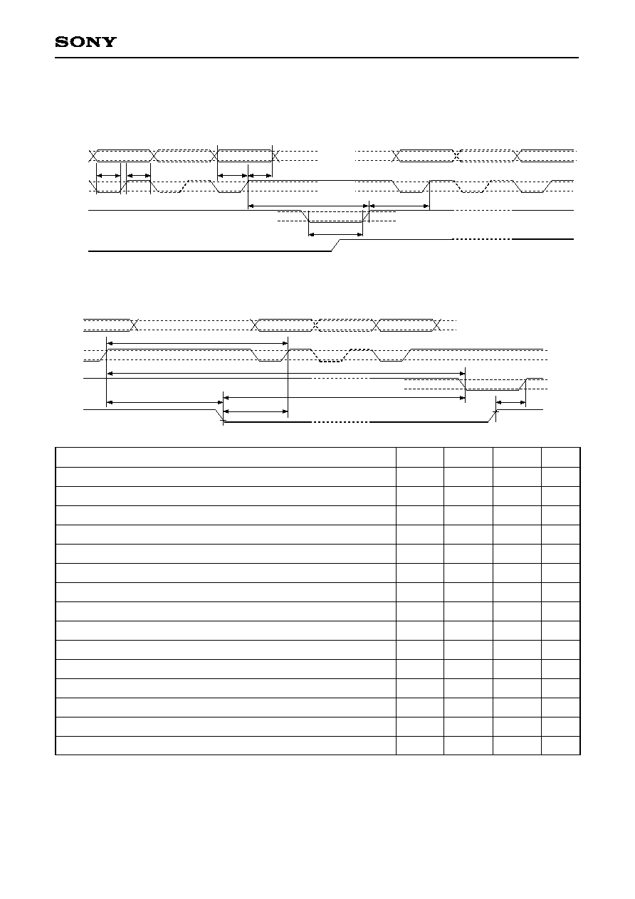
The definitions of signal timing required for control from the microcomputer are given below.
(4)-1. Initializing the Microcomputer Interface
The microcomputer interface must be initialized after resetting the IC.
After resetting the IC (t1
1/fs), input 16 SCK rising edges. After that, REDY goes Low within 4t + 50ns (t2),
and initialization is completed when REDY goes High again. Set RVDT Low while inputting SCK.
Note that the REDY Low time (t3) is a maximum of 1/fs. See the following page for the SCK restrictions. The
same restrictions apply as during data transfer.
When REDY goes Low due to initialization:
∑ The SCK for the first transfer can rise.
∑ The XLAT for the first transfer can fall.
However, the XLAT for the first transfer must rise after REDY goes High.
Fig. 5-2. Initialize Specifications
RVDT
XRST
SCK
REDY
t1
16 rising edges
t2
t3
Microcomputer interface can be used
≠ 20 ≠
CXD2719Q
(4)-2. Signal Timing
First, address section data and mode section data are sent from the microcomputer, synchronized to SCK, to
the RVDT pin.
The address section data is 8 bits for both the coefficient RAM and setup register, and the setup register has a
length of one word, so optional data can be transferred. Address section data is sent with LSB first.
Mode section data is fixed at 8 bits regardless of the transfer contents.
The phase relationship between SCK and RV data (data applied to the RVDT pin) has the following
restrictions:
∑ RV data must be established before SCK rises (tDS
20ns).
∑ RV data must be held for 1t + 20ns or more after SCK rises (tDH).
SCK itself has the following restrictions:
∑ SCK Low level must be 1t + 20ns or more (tSWL).
∑ SCK High level must be 1t + 20ns or more (tSWH).
After the SCK rise which corresponds to the mode section final data, XLAT rises (tSLP
20ns).
The XLAT Low level width must be maintained at 1t + 20ns or more (tLWL). The fall timing is restricted in that
even if REDY falls due to SCK during the preceding transfer, 3t + 20ns or more (tSLD) is required from the
SCK rise which corresponds to the data section final data.
Further, if preceding transfers have been performed and REDY = Low, XLAT must rise after REDY = High.
A0
A7
M0
M7
SQ00
SQ15
RVDT
SCK
XLAT
REDY
A0
M7
tDH
tDS
tSWH
tSWL
tSLD or tLWH
tLWL
tRLP
tLDR
tLSD
tSLP
tBSP
tSLP
tLDR
tRLP
tSS
tSLD
tSBD
D0/SQ00
D15/SQ15
Fig. 5-3. Write Timing
t is the cycle of 2/3 the clock frequency applied to the XTLI pin. (512fs)

≠ 21 ≠
CXD2719Q
Data section write begins after XLAT rises, and here also transfer must be performed with LSB first, with tDS
and tDH restrictions. In addition, after XLAT rises at the starting point for sending the data section, wait for 3t +
20ns or more for the first SCK rise (tLSD).
When 16 bits of this write is repeated, REDY goes Low within 4t + 50ns, and the microcomputer is informed of
waiting status for the SV cycle, which is the dedicated data rewrite cycle, by the microcomputer interface
(tSBD).
When REDY goes High again, the corresponding data is written.
The next communication can be restarted by using the REDY signal as follows.
∑ When REDY = Low, the SCK for the next transfer can rise (tBSP
20ns).
∑ In the same way, when REDY = Low, the XLAT for the next transfer can fall (tLDR
20ns).
REDY will fall due to this communication, but it is prohibited for XLAT to rise for the next transfer before REDY
rises. Make sure that the next XLAT rises after REDY rises (tRLP
20ns).
In order to restart the next transfer without using the REDY signal, the following conditions must be observed:
∑ There should be 2t + 40ns or more left between the SCK rise for the final data section and the SCK rise for
the next transfer (tSS).
∑ In the same way, the XLAT for the next transfer can fall after waiting for 3t + 20ns or more after the final
data section SCK rise (tSLD).
The tSS and tSLD here are shorter times than tSBD
4t + 50ns, so these are rather loose restrictions.
However, even in this case the XLAT rise for the next transfer must come after REDY rises (tRLP
20ns).
Further, the restriction for the XLAT fall at the starting point of this transfer from tSLD can be:
tSLD
3t + 20ns
≠ 22 ≠
CXD2719Q
6. Setup Register
When the setup register is selected in microcomputer interface transfer mode, the following settings are
possible for hardware such as the serial audio interface and DAC, and for software such as the Dolby Pro
Logic Surround decoder.
The setup register has a total of four fields, and 16 bits of setup information can be stored per field. However,
when this LSI is reset, the setup register contents are also reset to the settings shown in the "When reset"
column in Tables 6-1 to 6-4 below.
(1) Field A
SQA15
SQA14
SQA13
SQA12
SQA11,
SQA10
SQA09,
SQA08
SQA07,
SQA06
SQA05,
SQA04
SQA03 to
SQA00
DSP bypass mode
0: OFF
1: ON
Noise sequencer
0: OFF
1: ON
Reserve bit
Be sure to set both bits Low when changing the
setup register Field A se
Compensation filter
0: OFF
1: ON
Decimation ratio setting SQA11 SQA10
(SFC mode only)
0
0
: 1/1 (No decimation)
Be sure to also set
0
1
: 1/2 decimation
SQC07 and SQC06.
1
0
: 1/3 decimation
Dolby 3 Stereo
SQA09 SQA08
0
0
: OFF
0
1
: ON
Reserve bit
Be sure to set both bits Low when changing the
setup register Field A settings.
SFC mode
SQA05 SQA04
0
0
: OFF
0
1
: ON
Reserve bit
Be sure to set both bits Low when changing the
setup register Field A settings.
OFF
OFF
all "L"
OFF
1/1
(No decimation)
OFF
all "L"
OFF
all "L"
Table 6-1. Setup Register Field A
Bit names are indicated by the field name and the bit number. The bit names for Field A are SQA00 to
SQA15, and the first three letters of the bit names for Fields B, C and D are SQB, SQC and SQD,
respectively.
Data
section bit
Control contents
When reset
≠ 23 ≠
CXD2719Q
SQB15 to
SQB11
SQB10 to
SQB06
SQB05 to
SQB00
Center channel trim volume
00000: 0dB
(5 bits, analog)
00001: ≠1dB
00010: ≠2dB
11101: ≠29dB
11110: ≠30dB
11111: ≠31dB
Center channel trim volume
00000: 0dB
(5 bits, analog)
00001: ≠1dB
00010: ≠2dB
11101: ≠29dB
11110: ≠30dB
11111: ≠31dB
Reserve bit
Be sure to set all of these bits Low when
changing the setup register Field B settings.
0dB
0dB
all "L"
Table 6-2. Setup Register Field B
(2) Field B
Data
section bit
Control contents
When reset
≠ 24 ≠
CXD2719Q
SQC15
SQC14
SQC13
SQC12,
SQC11
SQC10
SQC09,
SQC08
SQC07,
SQC06
SQC05,
SQC04
SQC03 to
SQC00
LRCK format
0: normal
1: IIS
LRCK polarity selection 0: Lch "H"
1: Lch "L"
BCK polarity selection
0: Falling edge
relative to LRCK edge
1: Rising edge
Serial audio
SQC12 SQC11
interface setting
0
0
: MSB first/Frontward truncation/24 bits
0
1
: MSB first/Rearward truncation/16 bits
1
0
: MSB first/Rearward truncation/18 bits
1
1
: MSB first/Rearward truncation/20 bits
DAC forced mute
0: ON
1: OFF
Reserve bit
Be sure to set both bits Low when changing
the setup register Field C settings.
Decimation ratio setting SQC07 SQC06
(SFC mode only)
0
0
: 1/1 (No decimation)
Be sure to also set
0
1
: 1/2 decimation
SQA11 and SQA10.
1
: 1/3 decimation
BFOT output clock
SQC05 SQC04
frequency division
0
0
: 384Fs
ratio setting
0
1
: 256Fs
1
0
: 512Fs
1
1
: 768Fs
Reserve bit
Be sure to set all of these bits Low when changing
the setup register Field C settings.
normal
Lch "H"
Falling edge
MSB
first/Frontward
truncation/24 bits
ON
all "L"
1/1
(No decimation)
384Fs
all "L"
(3) Field C
Table 6-3. Setup Register Field C
Data
section bit
Control contents
When reset
Note) BCK polarity selection (SQC13) is valid only in slave mode. Fix to "0" in master mode.
Data
section bit
SQD15 to
SQD03
SQD02 to
SQD00
Control contents
Reserve bit
Be sure to set all of these bits Low when changing the
setup register Field D settings.
Be sure to set all of these bits Low
all "L"
all "L"
(4) Field D
Table 6-4. Setup Register Field D
When reset

≠ 25 ≠
CXD2719Q
7. Coefficient RAM
When the coefficient RAM is selected in microcomputer interface transfer mode, the various application
functions can be turned on and off, and the coefficient parameters such as each section's volume and delay
time can be set.
Coefficient RAM addresses other than those given in these specifications are "don't care". However, the RAM
is not cleared entirely when this LSI is reset, so there are no initial values as for the setup register. Be sure to
set all of the necessary data; otherwise misoperation may result.
The coefficient RAM has the capacitance of 256 words x 16 bits and the data transferred differs for each mode.
(See "8. Applications" for the detailed contents.)
8. Applications
The CXD2719Q is equipped with various applications such as Dolby Pro Logic Surround mode (Pro Logic
mode), Dolby 3 Stereo mode, noise sequencer mode, SFC mode, and DSP bypass mode.
The methods of setting each mode and of changing the mode are described below.
Note) The filter and other parameter values for each application assume a sampling frequency (fs) of 44.1 [kHz].
Consult your Sony representative with regard to use at other fs.
8-1. Dolby Pro Logic Surround Mode (Pro Logic Mode)
Pro Logic mode is realized using the adaptive matrix, passive decoder including BNR, auto input balance,
center channel mode control, simple SFC and other functions.
(1) Setting Pro Logic Mode
Pro Logic mode must be set by the following procedures in order to achieve stable adaptive matrix operation.
Setting Pro Logic mode by procedures other than those given below may aggravate the decoder
characteristics.
∑ Immediately after power-on reset
i)
Transfer the following setup data.
SQA = 0030H (Field A)
SQD = 7ee7H (Field D)
Note) Field C is "All 0", so the DAC forced mute is applied.
ii) Transfer the Pro Logic mode coefficient data.
iii) Transfer the setup data set in Pro Logic mode.
∑ Changing to Pro Logic mode from a different mode (other than Virtual mode)
i)
Apply the soft mute
1
in the current mode.
ii) Set the coefficients at the following addresses to "0000H".
Addresses: 6eH to 7fH
iii) Transfer the following setup data.
SQA = 0030H (Field A)
SQD = 7ee7H (Field D)
Note) The DAC forced mute is not applied by Field C.
iv) Transfer the Pro Logic mode coefficients for the soft mute status.
v) Transfer the setup data set in Pro Logic mode.
vi) Cancel the Pro Logic mode soft mute.
1
Soft mute: See "Appendix 1. Soft Mute".
≠ 26 ≠
CXD2719Q
(2) Setting Data
(2)-1. Setup Data
Table 8-1-1 lists the registers most closely related to Pro Logic mode.
Setup data not listed in Table 8-1-1 may be set as desired, with due consideration given to the contents of
Fields A to D noted in "6. Setup Register".
1: Noise sequencer mode
01: Dolby 3 Stereo mode
01: SFC mode
Center channel (C-ch) trim volume
Surround channel (S-ch) trim volume
SQA14
SQA09, 08
SQA05, 04
SQB15 to 11
SQB10 to 06
"0"
"00"
"00"
Don't care
Don't care
Register name Setting value
Remarks
Table 8-1-1. Pro Logic Mode Setup Register Settings
≠ 27 ≠
CXD2719Q
(2)-2. Coefficient Data
The coefficient data consists of "fixed values" shown in Table 8-1-2 and "setting values" shown in Table 8-1-3
which can be set by the user. All coefficient values must be sent to the coefficient RAM via the microcomputer
interface.
∑ Fixed values during Pro Logic mode initialization
The following fixed values must be set in the coefficient RAM to ensure proper internal operation.
Table 8-1-2. Pro Logic Mode Fixed Value Coefficients
27H
6dH
6eH
6fH
70H
71H
72H
73H
74H
75H
76H
77H
78H
79H
7aH
7bH
7cH
7dH
7eH
7fH
80H
81H
82H
83H
84H
85H
86H
87H
88H
89H
8aH
8bH
8cH
8dH
8eH
8fH
Address
0000H
051eH
ff86H
02a0H
f6c0H
2715H
4000H
5149H
e571H
0f4eH
f5b8H
075cH
fa97H
0402H
fd0bH
0225H
fe7cH
01d3H
f312H
4b85H
850fH
7d6bH
7d72H
22b6H
3a94H
0074H
7f18H
a000H
8000H
febfH
04f9H
eb83H
7b01H
cae0H
0400H
0074H
Fixed value
90H
91H
92H
93H
94H
95H
96H
97H
98H
99H
9aH
9bH
9cH
9dH
9eH
9fH
a0H
a1H
a2H
a3H
a4H
a5H
a6H
a7H
a8H
a9H
aaH
abH
acH
adH
aeH
b3H
b4H
b6H
b8H
b9H
Address
7f18H
0400H
001eH
7fc5H
0002H
7ffdH
8000H
dd1eH
da82H
109cH
2641H
3441H
dd1eH
109cH
da82H
2641H
3441H
0bbfH
e755H
4000H
f619H
e57eH
36dcH
5a82H
10c9H
2641H
7f18H
7e30H
4cbaH
c216H
0aa4H
27b4H
7e14H
7ff9H
0063H
0000H
Fixed value
baH
bbH
bcH
bdH
beH
bfH
c0H
c1H
c2H
c3H
c4H
c5H
c6H
c7H
c8H
c9H
caH
cbH
ccH
cdH
ceH
cfH
d0H
d1H
d2H
d3H
d5H
d7H
d8H
daH
dbH
deH
dfH
e3H
e4H
e5H
Address
43b9H
0400H
401eH
ec00H
8000H
a000H
0024H
ff92H
010aH
fce2H
097bH
e38dH
1555H
0400H
1400H
2000H
c000H
ffe4H
febcH
f520H
c144H
a57eH
0757H
0012H
7f00H
7fffH
fc00H
68a9H
5121H
7ff4H
7fe8H
8000H
c400H
0000H
0000H
0000H
Fixed value
e6H
e7H
e8H
e9H
eaH
ebH
ecH
edH
eeH
efH
f0H
f9H
feH
ffH
Address
0000H
0000H
0000H
0000H
0000H
0000H
0000H
0000H
0000H
0000H
7fffH
8000H
b800H
0001H
Fixed value

≠ 28 ≠
CXD2719Q
∑ Pro Logic mode user setting coefficients
The relationships between the coefficient RAM and each function during Pro Logic mode operation are as
follows.
00H
01H
02H
03H
04H
05H
06H
07H
08H
09H
0aH
0bH
0cH
0dH
0eH
0fH
10H
11H
12H
13H
14H
15H
16H
17H
18H
19H
1aH
1bH
1cH
1dH
1eH
1fH
20H
21H
22H
23H
24H
KLV
KRV
KCV
KSV
KLm1
KRm1
a0
a1
b
KLm2
KRm2
a0
a1
b
KLd
KRd
KCd
KSd
Kfb
a0
a1
b
a0
a1
b
KDin
TP1
TP2
TP3
TP4
TP5
TP6
KDout
KDV1
KDV2
KDV3
KLRm1
Simple SFC: L-ch dry
L-ch mix volume
Simple SFC: R-ch dry
R-ch mix volume
Simple SFC: C-ch
C-ch volume
Simple SFC: S + L/R (HPF1)
S-ch mix volume
Simple SFC: L-ch
LPF1 mix volume
Simple SFC: R-ch
LPF1 mix volume
Simple SFC: LPF1 coefficient
Simple SFC: LPF1 coefficient
Simple SFC: LPF1 coefficient
Simple SFC: L-ch
HPF1 mix volume
Simple SFC: R-ch
HPF1 mix volume
Simple SFC: HPF1 coefficient
Simple SFC: HPF1 coefficient
Simple SFC: HPF1 coefficient
Simple SFC: L-ch
Delay RAM mix volume
Simple SFC: R-ch
Delay RAM mix volume
Simple SFC: C-ch
Delay RAM mix volume
Simple SFC: S-ch
Delay RAM mix volume
Simple SFC: Delay RAM feedback volume
Simple SFC: HPF2 coefficient
Simple SFC: HPF2 coefficient
Simple SFC: HPF2 coefficient
Simple SFC: LPF2 coefficient
Simple SFC: LPF2 coefficient
Simple SFC: LPF2 coefficient
Simple SFC: Delay RAM write address
Simple SFC: Delay RAM read Tap1 address
Simple SFC: Delay RAM read Tap2 address
Simple SFC: Delay RAM read Tap3 address
Simple SFC: Delay RAM read Tap4 address
Simple SFC: Delay RAM read Tap5 address
Simple SFC: Delay RAM read Tap6 address
Simple SFC: Delay RAM feedback Tap address
Simple SFC: Delay RAM
S-ch mix volume
Simple SFC: Delay RAM
R-ch mix volume
Simple SFC: Delay RAM
L-ch mix volume
Simple SFC: LPF1
L-ch mix volume
See Table 8-1-13.
See Table 8-1-13.
See Table 8-1-13.
See Table 8-1-13.
See Table 8-1-13.
See Table 8-1-13.
See Table 8-1-16.
See Table 8-1-16.
See Table 8-1-16.
See Table 8-1-13.
See Table 8-1-13.
See Table 8-1-16.
See Table 8-1-16.
See Table 8-1-16.
See Table 8-1-13.
See Table 8-1-13.
See Table 8-1-13.
See Table 8-1-13.
See Table 8-1-13.
See Table 8-1-16.
See Table 8-1-16.
See Table 8-1-16.
See Table 8-1-16.
See Table 8-1-16.
See Table 8-1-16.
See Table 8-1-15.
See Table 8-1-15.
See Table 8-1-15.
See Table 8-1-15.
See Table 8-1-15.
See Table 8-1-15.
See Table 8-1-15.
See Table 8-1-15.
See Table 8-1-13.
See Table 8-1-13.
See Table 8-1-13.
See Table 8-1-13.
Table 8-1-3 (1). Pro Logic Mode Setting Value Coefficients
Address
Symbol
Function
Setting value
≠ 29 ≠
CXD2719Q
25H
26H
28H
29H
2aH
2bH
2cH
2dH
afH
b0H
b1H
b2H
b5H
b7H
d4H
d6H
d9H
dcH
ddH
f2H
f3H
f4H
f5H
f6H
f7H
f8H
faH
fbH
Address
KLRm2
KLRm3
KTP1
KTP2
KTP3
KTP4
KTP5
KTP6
b2
b1
a
≠a
aslw
2D
Kx
KiA
Ke
Kia
Kis
KL
KR
KH
KP
KCH
KCP
KS
Kdlb
Dly
Symbol
Simple SFC: LPF1
R-ch mix volume
Simple SFC: HPF1
S-ch mix volume
Simple SFC: Tap1 volume
Simple SFC: Tap2 volume
Simple SFC: Tap3 volume
Simple SFC: Tap4 volume
Simple SFC: Tap5 volume
Simple SFC: Tap6 volume
7K LPF parameter
7K LPF parameter
7K LPF parameter
7K LPF parameter
Passive decoder M-BNR
Passive decoder M-BNR
Auto input balance ON/OFF
Serial audio interface input volume
De-emphasis ON/OFF
Analog input mix volume
Digital input mix volume
Center mode control volume
Center mode control volume
Center mode control volume
Center mode control volume
Center mode control volume
Center mode control volume
Passive decoder volume
Passive decoder M-BNR ON/OFF
Passive decoder delay time adjustment
Function
See Table 8-1-13.
See Table 8-1-13.
See Table 8-1-13.
See Table 8-1-13.
See Table 8-1-13.
See Table 8-1-13.
See Table 8-1-13.
See Table 8-1-13.
0000 = OFF, df66 = ON
0000 = OFF, 5723 = ON
0000 = OFF, 125e = ON
8000 = OFF, eda2 = ON
See Table 8-1-12.
See Table 8-1-12.
0000 = OFF, 00ff = ON
See Table 8-1-5.
0000 = OFF, ac19 = ON
See Table 8-1-4.
See Table 8-1-5.
See Tables 8-1-7, 8.
See Tables 8-1-7, 8.
See Tables 8-1-7, 8.
See Tables 8-1-7, 8.
See Tables 8-1-7, 8.
See Tables 8-1-7, 8.
See Table 8-1-8.
0000 = OFF, 2000 = ON
See Table 8-1-9.
Setting value
Table 8-1-3 (2). Pro Logic Mode Setting Value Coefficients
≠ 30 ≠
CXD2719Q
(2)-3. Signal Flow for Dolby Pro Logic Mode
L
P
F
A
D
C
D
e
c
i
m
a
t
i
o
n
D
C
C
u
t
L
P
F
A
D
C
D
e
c
i
m
a
t
i
o
n
D
C
C
u
t
D
e
E
m
p
h
a
s
i
s
L
I
N
R
I
N
S
I
A
1
S
I
A
2
D
e
E
m
p
h
a
s
i
s
≠
K
i
A
(
d
6
H
)
≠
K
i
A
(
d
6
H
)
≠
K
i
a
(
d
c
H
)
≠
K
i
s
(
d
d
H
)
≠
K
i
a
(
d
c
H
)
≠
K
i
s
(
d
d
H
)
L
t
L
R
C
S
R
t
P
r
o
L
o
g
i
c
D
e
c
o
d
e
r
L
L
R
C
S
S
S
i
m
p
l
e
S
F
C
R
C
D
A
C
D
A
C
O
v
e
r
S
a
m
p
l
i
n
g
O
v
e
r
S
a
m
p
l
i
n
g
D
A
C
D
A
C
O
v
e
r
S
a
m
p
l
i
n
g
O
v
e
r
S
a
m
p
l
i
n
g
L
P
F
L
P
F
M
U
X
&
L
P
F
M
U
X
&
L
P
F
T
r
i
m
V
o
l
L
O
U
T
R
O
U
T
X
C
O
U
T
X
S
O
U
T
T
r
i
m
V
o
l
Fig. 8-1-1
≠ 31 ≠
CXD2719Q
(3) Volume Coefficient Settings
[Relevant data] Coefficients: KiA (d6H), Kia (dcH), Kis (ddH)
The I/O levels and volumes are 2's complement format with a decimal point between D15 and D14, and
hexadecimal notation with D15 as MSB and D0 as LSB.
The coefficient and level relationships are as follows.
D15 to D0 are negative values, but the DSP calculation is (≠1)
◊
(D15 to D0).
(3)-1. Kia (dcH): 0dB = c000H
The I/O levels for 8000H to ffffH are obtained by the following formulas.
(Coefficient value) = [(≠1)
◊
D15 +
(Dn
◊
2
n ≠ 15
)]
◊
(≠2)
I/O level = 20 log [coefficient value] dB
(3)-2. KiA (d6H), Kis (ddH): 0dB = 8000H
The I/O levels for 8000H to ffffH are obtained by the following formulas.
(Coefficient value) = [(≠1)
◊
D15 +
(Dn
◊
2
n ≠ 15
)]
◊
(≠1)
I/O level = 20 log [coefficient value] dB
Unless otherwise specified, subsequent setting examples (Pro Logic mode) in these specifications assume
either:
Kia = d2b2H, KiA = 0000H, Kis = 0000H
or:
Kia = 0000H, KiA = 8000H, Kis = a563H
(4) Auto Input Balance Control
[Relevant data] Coefficient: Kx (d4H)
The auto input balance function is turned on and off by coefficient Kx (d4H).
8000H
a599H
c000H
d2b2H
e000H
eff6H
ffffH
0000H
D15 to D0
+6.02
+3.00
0.00
≠3.00
≠6.02
≠12.00
≠84.29
≠
Level [dB]
8000H
a563H
c000H
e000H
ffffH
0000H
D15 to D0
0.00
≠3.00
≠6.02
≠12.04
≠90.31
≠
Level [dB]
14
n = 0
14
n = 0
Table 8-1-4. Kia (dcH) Setting Value Examples
Table 8-1-5. KiA (d6H), Kis (ddH) Setting Value Examples
Coefficient
Kx (d4H)
OFF = 0000H
ON = 00ffH
Table 8-1-6. Auto Input Balance ON/OFF
≠ 32 ≠
CXD2719Q
(5) Center Mode Control
[Relevant data] Coefficients: KP (f5H), KH (f4h), KL (f2H), KR (f3H), KCP (f7H), KCH (f6H)
The center channel output mode can be set to Normal, Wide or Phantom mode as shown in Table 8-1-7 below.
Coefficient
KP (f5H)
e000H
0000H
e000H
KH (f4H)
e000H
0000H
0000H
KL (f2H)
d2cdH
d2cdH
d2cdH
KR (f3H)
d2cdH
d2cdH
d2cdH
KCP (f7H)
0000H
e000H
0000H
KCH (f6H)
e000H
0000H
0000H
Mode
Normal
Wide
Phantom
Table 8-1-7. Center Mode Control Setting Value Examples
LP
RP
CP
≠KL (f2H)
≠KR (f3H)
LO
RO
CO
LPF
HPF
≠KCH (f6H)
≠KCP (f7H)
Note) If KH is set to 0000H in Phantom center channel mode, the LPF is set to
data through status and the data added to the L and R channels is CP
◊
KP.
≠KH (f4H), ≠KP (f5H)
Fig. 8-1-2. Signal Flow for Center Mode Control (L, R, C-ch)
Note) In Phantom center channel mode, the center channel information is divided equally between the left and
right speakers.
8000H
c000H
d2cdH
e000H
e959H
eff6H
f7f6H
ffffH
0000H
D15 to D0
+12.04
+6.02
+3.00
0
≠3.00
≠6.00
≠12.00
≠78.27
≠
Level [dB]
Table 8-1-8. KP, KH, KL, KR, KCP, KCH and KS
Setting Value Examples
The level of each channel can be adjusted by changing
the KP, KH, KL, KR, KCP and KCH setting values. In
these cases, be sure to change only the shaded portions
for each mode in Table 8-1-7.
However, make sure that KP = KH in Normal mode. In
Phantom mode, set KH to 0000H and adjust the mix level
to the left and right channels using KP.
The I/O levels for 8000H to ffffH are obtained by the
following formulas.
(Coefficient value) = [(≠1)
◊
D15 +
(Dn
◊
2
n ≠ 15
)]
◊
(≠4)
I/O level = 20 log [coefficient value] dB
14
n = 0
In Table 8-1-7, lowering the input level by 3dB using Kia (dcH) or Kis (ddH) raises the output level of the L
and R channels by 3dB. In this case, attaching external parts as shown in the Application Circuit is
recommended to increase the C and S channel gains.
≠ 33 ≠
CXD2719Q
(6) Passive Decoder (Surround Channel)
The surround channel is processed according to the flow shown in Fig. 8-1-3.
The setting method for each section is described below.
SP
≠KS (f8H)
SO
7kHz
LPF
M-BNR
Delay
Fig. 8-1-3. Passive Decoder Signal Flow (S-ch)
0020H
0040H
∑
∑
52b0H
∑
6e40H
∑
89d0H
∑
a560H
∑
∑
bf80H
bfa0H
Setting value Dly (fbH)
ON
OFF
df66
0000
b2
5723
0000
b1
125e
0000
a
eda2
8000
≠a
0.022ms
0.045ms
∑
∑
15.000ms
∑
20.000ms
∑
25.000ms
∑
30.000ms
∑
∑
34.739ms
34.762ms
Delay (fs = 44.1kHz)
Table 8-1-9. Surround Channel (S-ch) Delay Time Setting
Value Examples
(6)-1. Delay Time Setting
[Relevant data] Coefficient: Dly (fbH)
The surround channel delay time can be varied
by setting the coefficient Dly value. (Dly is the
delay line read address.)
Only the upper 11 of the 16 coefficient bits are
used. The lower 5 bits are not used, and are
ignored even if set.
That is to say, Dly can be set in 0020H
increments, and the delay time can be set in
approximately 0.022 ms increments.
The following condition also applies.
∑ 0020H
Dly
bfa0H
The coefficient value is calculated as follows.
(Dly)
Decimal
= (Delay [s]
◊
fs [Hz]
◊
32
Example) For 20ms (fs = 44100 [Hz])
0.02
◊
44100
◊
32 = 28224 6e40H
(6)-2. 7kHz Low-Pass Filter
[Relevant data] Coefficients: b2 (afH), b1 (b0H), a (b1H), ≠a (b2H)
The 7kHz LPF of the passive decoder can be turned on and off by setting the coefficients in Table 8-1-10.
Table 8-1-10. Passive Decoder 7kHz LPF ON/OFF Setting
Hexadecimal conversion
≠ 34 ≠
CXD2719Q
(6)-3. Modified Dolby B-type NR
[Relevant data] Coefficients: aslw (b5H), 2D (b7H), KiA (d6H), Kia (dcH), Kis (ddH), Kdlb (faH)
The aslw and 2D coefficients and the ON/OFF coefficient Kdlb must be set for Modified Dolby B-type NR.
This function is turned on and off by setting Kdlb as shown in Table 8-1-11. The aslw and 2D coefficient values
differ according to the Dolby level, prefilter and coefficient Kia/Kis (KiA) conditions. Table 8-1-12 shows typical
setting value examples based on these three conditions. The prefilter gain (= ≠3.52dB) is the value when using
the Application Circuit given in these specifications.
Consult your Sony representative with regard to use under conditions other than those noted in Table 8-1-12.
Coefficient
Kdlb (faH)
OFF = 0000H
ON = 2000H
Prefilter
Dolby level
Kia (dcH)
Kis (ddH)
aslw (b5H)
2D (b7H)
Table 8-1-11. Modified Dolby B-type NR ON/OFF Setting
Table 8-1-12. Modified Dolby B-type NR Coefficient Value Examples for Different Input Level Conditions
(during digital input: KiA (d6H) = 8000H)
(6)-4. Volume
[Relevant data] Coefficient: KS (f8H)
The KS (f8H) volume values are as shown in Table 8-1-8. See "5. Center Mode Control" for the calculation
method.
≠3.52dB
≠3.52dB
≠3.52dB
(Digital input)
300mVrms
300mVrms
200mVrms
≠20dBFS
d2b2H
c000H
d2b2H
0000H
0000H
0000H
0000H
a563H
00caH
009eH
00caH
00caH
0033H
004aH
0023H
0023H
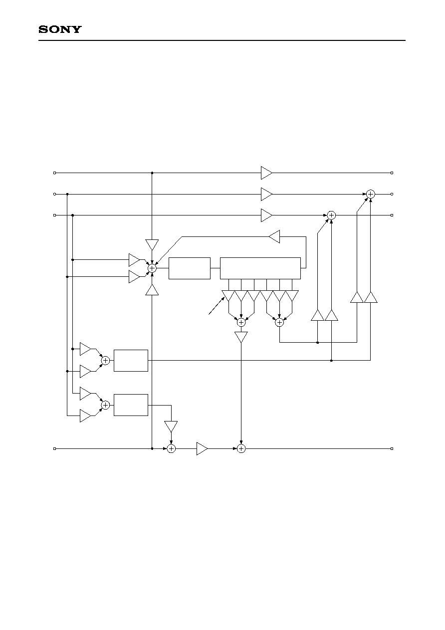
≠ 35 ≠
CXD2719Q
(7) Simple SFC
Simple SFC effects can be added after Dolby Pro Logic Surround decoder processing. (See Fig. 8-1-1.)
Fig. 8-1-4 shows the signal flow for the simple SFC block.
When not using simple SFC, set the coefficients as follows to set the simple SFC block to through status.
KLV (00H), KRV (01H), KCV (02H), KSV (03H) = 8000H
KDV1 (21H), KDV2 (22H), KDV3 (23H), KLRm1 (24H), KLRm2 (25H), KLRm3 (26H) = 0000H
C
L
≠KCV (02H)
≠KLV (00H)
R
≠KRV (01H)
S
≠KSV (03H)
LPF1
06H to 08H
HPF1
0bH to 0dH
≠KLm2 (09H)
≠KSd (11H)
HPF2 + LPF2
13H to 18H
≠KDV1 (21H)
Delay
KDin
KDout
TP1 TP2 TP3 TP4 TP5 TP6
≠Kfb (12H)
C
L
R
1
2
3
4
5
6
≠KTP1 to ≠KTP6
(28H to 2dH)
≠KRm2 (0aH)
≠KLm1 (04H)
≠KRm1 (05H)
≠KLRm3 (26H)
≠KCd (10H)
≠KRd (0fH)
≠KLd (0eH)
S
≠KDV2
(22H)
≠KLRm2
(25H)
≠KDV3
(23H)
≠KLRm1
(24H)
Fig. 8-1-4. Simple SFC Signal Flow
≠ 36 ≠
CXD2719Q
(7)-1. Volume Settings for Each Section
[Relevant data] Coefficients: KLV (00H), KRV (01H), KCV (02H), KSV (03H), KLm1 (04H), KRm1 (05H),
KLm2 (09H), KRm2 (0aH), KLd (0eH), KRd (0fH), KCd (10H), KSd (11H),
Kfb (12H), KDV1 (21H), KDV2 (22H), KDV3 (23H), KLRm1 (24H),
KLRm2 (25H), KLRm3 (26H), KTP1 (28H), KTP2 (29H), KTP3 (2aH),
KTP4 (2bH), KTP5 (2cH), KTP6 (2dH)
The format is the same as that described in "(3) Volume Coefficient Settings". The levels are as follows when
0dB = 8000H.
The I/O levels for 8000H to ffffH are obtained by the following formulas.
(Coefficient value) = [(≠1)
◊
D15 +
(Dn
◊
2
n ≠ 15
)]
◊
(≠1)
I/O level = 20 log [coefficient value] dB
The above coefficients are normally applied as negative values, but positive values should be applied when
intentionally inverting the phase with TP1 to TP6, etc. In this case, the levels are as follows when 0dB = 7fffH.
The I/O levels for 7fffH to 0001H are obtained by the following formulas.
(Coefficient value) = [D15 +
(Dn
◊
2
n ≠ 15
)]
I/O level = 20 log [coefficient value] dB
8000H
a563H
c000H
d2b2H
e000H
f000H
ffffH
0000H
D15 to D0
0.00
≠3.00
≠6.02
≠9.02
≠12.04
≠18.06
≠90.31
≠
Level [dB]
14
n = 0
14
n = 0
Table 8-1-13. Setting Value Examples for Each Volume
(Negative Values)
7fffH
5a9dH
4000H
2d4eH
2000H
1000H
0001H
0000H
D15 to D0
0.00
≠3.00
≠6.02
≠9.02
≠12.04
≠18.06
≠90.31
≠
Level [dB]
Table 8-1-14. Setting Value Examples for Each Volume
(Positive Values)
≠ 37 ≠
CXD2719Q
(7)-2. Delay Line Settings
[Relevant data] Coefficients: KDin (19H), TP1 (1aH), TP2 (1bH), TP3 (1cH), TP4 (1dH), TP5 (1eH),
TP6 (1fH), KDout (20H)
The Pro Logic mode delay lines are used for both the passive decoder short delay and the simple SFC
reverberation, and are thus subject to the following restrictions:
∑ Dly + 0020H
KDin (0020H
Dly
KDin ≠ 0020H)
∑ 0020H
TP
KDout
∑ KDin + KDout
bfe0H
Dly (fbH): Pro Logic delay line read address
KDin (19H): Simple SFC delay line write address
TP1 to TP6 (1aH to 1fH): Simple SFC tap read addresses (determine the delay time for each tap)
KDout (20H): Simple SFC feedback loop read address (determines the maximum delay time)
Note) The minimum unit for all the above coefficients is "0020H". Values smaller than this are ignored.
0020H
0040H
∑
∑
1a60H
∑
35f0H
∑
5180H
∑
6d10H
∑
∑
bf80H
bfa0H
Setting value
KDout, TP1 to TP6
0.022ms
0.045ms
∑
∑
4.784ms
∑
9.784ms
∑
14.784ms
∑
19.784ms
∑
∑
34.739ms
34.762ms
Delay
(fs = 44.1kHz)
The TP1 to TP6 and KDout addresses are specified in a different
manner than Dly and KDin. These addresses are specified by the
address value assuming KDin as the reference (= 0000H).
That is to say, the actual address is KDin + KDout, etc.
The coefficient values are calculated as follows.
(Dly)
Decimal
= (Delay [s])
◊
fs [Hz]
◊
32
Example) When using 20ms for the passive decoder, and all
remaining delay lines as reverberation
20ms
Dly = 6e40H
KDin = 6e40H + 0020H = 6e60H
KDout = bfe0H ≠ 6e60H = 5180H
0020H
TP1 to 6
5180H
Table 8-1-15. Simple SFC Delay Time Setting
Value Examples
0000H
20.0ms
14.8ms
6e40H
6e60H
5180H
Passive decoder
Simple SFC
Dly
KDin
KDout
34.8ms (0000H to bfe0H)
Fig. 8-1-5. Pro Logic Mode Delay Line Setting Example
≠ 38 ≠
CXD2719Q
(7)-3. Filters
[Relevant data] Coefficients: a0 (06H, 0bH, 13H, 16H), a1 (07H, 0cH, 14H, 17H), b (08H, 0dH, 15H, 18H)
LPF1, HPF1, LPF2 and HPF2 are comprised of primary IIR filters, and the coefficient setting and cut-off
frequency relationship are as shown in Table 8-1-16.
Table 8-1-16. Simple SFC HPF and LPF Setting Coefficients
100
200
300
400
500
600
700
800
900
1000
1200
1400
1600
1800
2000
2200
2400
2600
2800
3000
3200
3400
3600
3800
4000
4200
4400
4600
4800
5000
FF19
FE34
FD53
FC74
FB99
FAC1
F9EB
F918
F848
F77A
F5E6
F45C
F2DB
F162
EFF2
EE89
ED28
EBCE
EA7A
E92D
E7E6
E6A5
E569
E432
E301
E1D4
E0AB
DF87
DE67
DD4B
a0
a1
b
a0
a1
b
00E7
01CC
02AD
038C
0467
053F
0615
06E8
07B8
0886
0A1A
0BA4
0D25
0E9E
100E
1177
12D8
1432
1586
16D3
181A
195B
1A97
1BCE
1CFF
1E2C
1F55
2079
2199
22B5
7E30
7C67
7AA4
78E7
7731
7580
73D4
722E
708E
6EF2
6BCB
68B6
65B4
62C3
5FE2
5D11
5A4E
579A
54F3
5259
4FCB
4D48
4AD0
4863
4600
43A6
4155
3F0D
3CCD
3A94
80E8
81CD
82AE
838D
8468
8540
8616
86E9
87B9
8887
8A1B
8BA5
8D26
8E9F
900F
9178
92D9
9433
9587
96D4
981B
995C
9A98
9BCF
9D00
9E2D
9F56
A07A
A19A
A2B6
7F18
7E33
7D52
7C73
7B98
7AC0
79EA
7917
7847
7779
75E5
745B
72DA
7161
6FF1
6E88
6D27
6BCD
6A79
692C
67E5
66A4
6568
6431
6300
61D3
60AA
5F86
5E66
5D4A
7E30
7C67
7AA4
78E7
7731
7580
73D4
722E
708E
6EF2
6BCB
68B6
65B4
62C3
5FE2
5D11
5A4E
579A
54F3
5259
4FCB
4D48
4AD0
4863
4600
43A6
4155
3F0D
3CCD
3A94
Cut-off
frequency [Hz]
LPF1, 2
HPF1, 2
5200
5400
5600
5800
6000
6200
6400
6600
6800
7000
7200
7400
7600
7800
8000
8200
8400
8600
8800
9000
9200
9400
9600
9800
10000
10200
10400
10600
10800
11000
OFF
DC32
DB1D
DA0C
D8FD
D7F2
D6E9
D5E3
D4DF
D3DE
D2DF
D1E3
D0E8
CFEF
CEF8
CE03
CD0F
CC1D
CB2B
CA3B
C94D
C85F
C772
C685
C59A
C4AF
C3C5
C2DA
C1F1
C107
C01E
8000
a0
a1
b
a0
a1
b
23CE
24E3
25F4
2703
280E
2917
2A1D
2B21
2C22
2D21
2E1D
2F18
3011
3108
31FD
32F1
33E3
34D5
35C5
36B3
37A1
388E
397B
3A66
3B51
3C3B
3D26
3E0F
3EF9
3FE2
0000
3863
3639
3416
31F9
2FE2
2DD0
2BC4
29BD
27BB
25BD
23C4
21CF
1FDD
1DEF
1C04
1A1C
1838
1655
1475
1298
10BC
0EE2
0D09
0B32
095C
0788
05B3
03E0
020D
003A
0000
A3CF
A4E4
A5F5
A704
A80F
A918
AA1E
AB22
AC23
AD22
AE1E
AF19
B012
B109
B1FE
B2F2
B3E4
B4D6
B5C6
B6B4
B7A2
B88F
B97C
BA67
BB52
BC3C
BD27
BE10
BEFA
BFE3
8000
5C31
5B1C
5A0B
58FC
57F1
56E8
55E2
54DE
53DD
52DE
51E2
50E7
4FEE
4EF7
4E02
4D0E
4C1C
4B2A
4A3A
494C
485E
4771
4684
4599
44AE
43C4
42D9
41F0
4106
401D
0000
3863
3639
3416
31F9
2FE2
2DD0
2BC4
29BD
27BB
25BD
23C4
21CF
1FDD
1DEF
1C04
1A1C
1838
1655
1475
1298
10BC
0EE2
0D09
0B32
095C
0788
05B3
03E0
020D
003A
0000
Cut-off
frequency [Hz]
LPF1, 2
HPF1, 2
≠ 39 ≠
CXD2719Q
8-2. Dolby 3 Stereo Mode
This mode is a part of the Pro Logic adaptive matrix functions.
Specifically, surround output is muted and surround signal directionality is not harmonized.
(1) Setting Dolby 3 Stereo Mode
Dolby 3 Stereo mode must be set by the following procedures in order to achieve stable adaptive matrix
operation. Setting Dolby 3 Stereo mode by procedures other than those given below may aggravate the
decoder characteristics.
∑ Immediately after power-on reset
i)
Transfer the following setup data.
SQA = 0030H (Field A)
SQD = 7ee7H (Field D)
Note) Field C is "All 0", so the DAC forced mute is applied.
ii) Transfer the Dolby 3 Stereo mode coefficient data.
iii) Transfer the setup data set in Dolby 3 Stereo mode.
∑ Changing to Dolby 3 Stereo mode from a different mode
i) Apply the soft mute in the current mode.
ii) Set the coefficients at the following addresses to "0000H".
Addresses: 6eH to 7fH
iii) Transfer the following setup data.
SQA = 0030H (Field A)
SQD = 7ee7H (Field D)
Note) The DAC forced mute is not applied by Field C.
iv) Transfer the Dolby 3 Stereo mode coefficients for the soft mute status.
v) Transfer the setup data set in Dolby 3 Stereo mode.
vi) Cancel the Dolby 3 Stereo mode soft mute.
(2) Setting Data
(2)-1. Setup Data
Table 8-3-1 lists the registers most closely related to Dolby 3 Stereo mode.
Setup data not listed in Table 8-3-1 may be set as desired, with due consideration given to the contents of
Fields A to D noted in "6. Setup Register".
1: Noise sequencer mode
01: Dolby 3 Stereo mode
01: SFC mode
Center channel (C-ch) trim volume
SQA14
SQA09, 08
SQA05, 04
SQB15 to 11
"0"
"01"
"00"
Don't care
Table 8-2-1. Dolby 3 Stereo Mode Setup Register Settings
(2)-2. Coefficient Data
The coefficient data used in Dolby 3 Stereo mode is entirely the same as that for Pro Logic mode. See "8-1.
Dolby Pro Logic Surround Mode".
Register name Setting value
Remarks
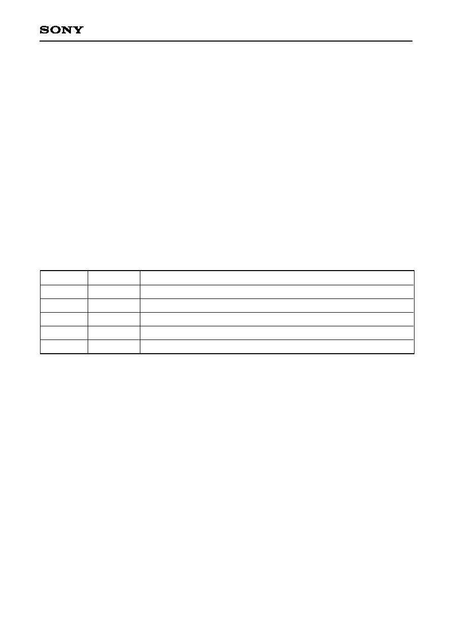
≠ 40 ≠
CXD2719Q
8-3. Noise Sequencer Mode
(1) Setting Noise Sequencer Mode
Set noise sequencer mode by the following procedures.
∑ Immediately after power-on reset
i)
Transfer the setup data set in noise sequencer mode.
ii) Transfer the noise sequencer mode coefficient data.
∑ Changing to noise sequencer mode from a different mode
i)
Apply the soft mute in the current mode.
ii) Transfer the setup data set in noise sequencer mode.
iii) Transfer the noise sequencer mode coefficient data.
(2) Setting Data
(2)-1. Setup Data
Table 8-3-1 lists the registers most closely related to noise sequencer mode.
Setup data not listed in Table 8-3-1 may be set as desired, with due consideration given to the contents of
Fields A to D noted in "6. Setup Register".
1: Noise sequencer mode
01: Dolby 3 Stereo mode
01: SFC mode
Center channel (C-ch) trim volume
Surround channel (S-ch) trim volume
SQA14
SQA09, 08
SQA05, 04
SQB15 to 11
SQB10 to 06
"1"
"00"
"00"
Don't care
Don't care
Register name Setting value
Remarks
Table 8-3-1. Noise Sequencer Mode Setup Register Settings
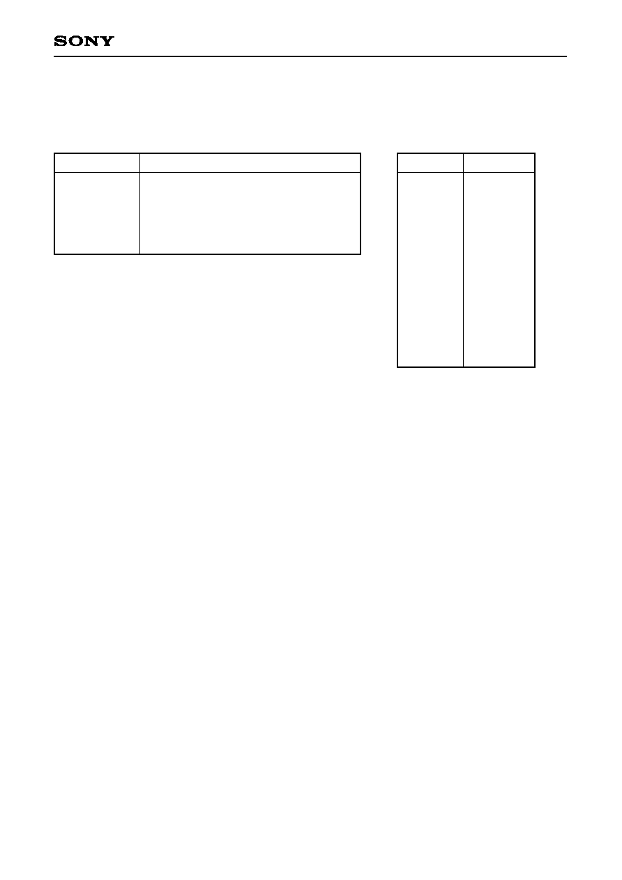
≠ 41 ≠
CXD2719Q
(2)-2. Coefficient Data
In noise sequencer mode, change the coefficients from addresses d0H to e2H of Pro Logic mode as shown in
the table below. The other coefficients may be left as the Pro Logic mode coefficient settings.
L-ch
C-ch
R-ch
S-ch
L
C
R
S
L
C
R
2000
0000
0000
0000
2000
2000
T1 (d0H)
2000
3000
0000
0000
3000
3000
T2 (d1H)
2000
3000
4000
0000
4000
4000
T3 (d2H)
2000
3000
4000
5000
5000
4000
T4 (d3H)
d4H
d5H
d6H
d7H
d8H
d9H
daH
dbH
dcH
ddH
deH
dfH
e0H
e1H
e2H
Address
1000H
0040H
c000H
d2b1H
0000H
2d4fH
0000H
d2b1H
c000H
d2b1H
8000H
7789H
6f12H
0876H
6f14H
Fixed value
Table 8-3-2. Noise Sequencer Mode Coefficient Setting Values
Table 8-3-3. Noise Sequencer Mode
Coefficient Fixed Values
(3) Output Level Adjustment
[Relevant data] Coefficients: KL (f2H), KR (f3H), KH (f4H), KP (f5H), KCH (f6H), KCP (f7H), KS (f8H)
The noise output level in noise sequencer mode is adjusted by the center mode control coefficients (f2H to
f7H) and the passive decoder volume coefficient (f8H)
See (5) and (6)-4 of "8-1. Pro Logic Mode".
8-4. SFC Mode
SFC mode is used for 2-channel stereo input, and realizes reverberation effects using the delay lines, and
dynamics processing using 1/2 and 1/3 decimation and the compressor.
This is a separate application from the simple SFC of Pro Logic mode.
(1) Setting SFC Mode
Set SFC mode by the following procedures.
∑ Immediately after power-on reset
i)
Transfer the setup data set in SFC mode.
ii) Transfer the SFC mode coefficient data.
∑ Changing to SFC mode from a different mode
i)
Apply the soft mute in the current mode.
ii) Transfer the setup data set in SFC mode.
iii) Transfer the SFC mode coefficient data.
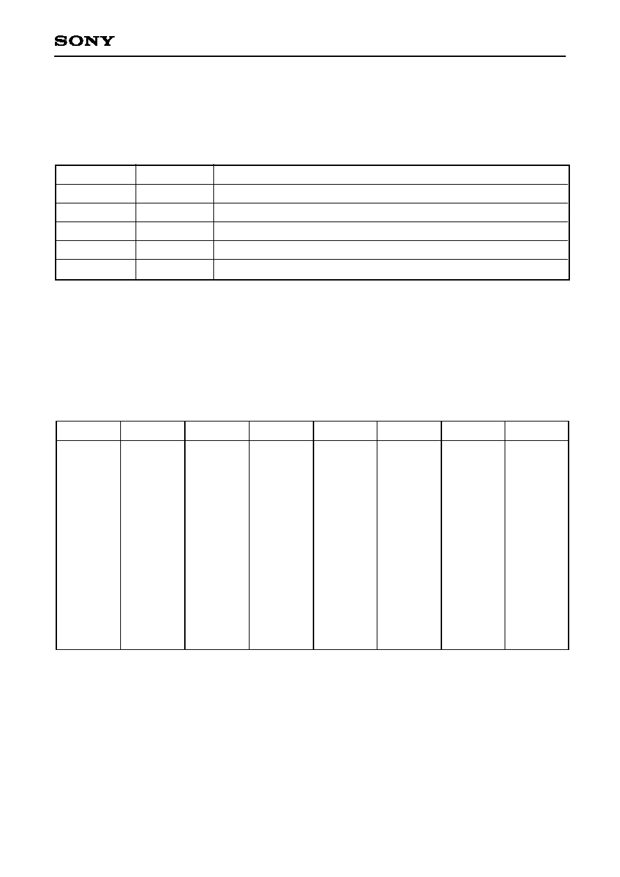
≠ 42 ≠
CXD2719Q
(2) Setting Data
(2)-1. Setup Data
Table 8-4-1 lists the registers most closely related to SFC mode.
Setup data not listed in Table 8-4-1 may be set as desired, with due consideration given to the contents of
Fields A to D noted in "6. Setup Register".
00: No decimation, 01: 1/2, 10: 1/3
01: SFC mode
Center channel (C-ch) trim volume
Surround channel (S-ch) trim volume
00: No decimation, 01: 1/2, 1
: 1/3
SQA11, 10
SQA05, 04
SQB15 to 11
SQB10 to 06
SQC07, 06
Don't care
"01"
Don't care
Don't care
Don't care
Register name
Setting value
Remarks
Table 8-4-1. SFC Mode Setup Register Settings
(2)-2. Coefficient Data
The SFC mode coefficient data uses the RAM for the entire area. Also, like other modes, the coefficient data
consists of fixed values and setting values.
∑ Fixed values during SFC mode initialization
The following fixed values must be set in the coefficient RAM to ensure proper DSP internal operation.
00H
01H
38H
39H
3aH
3bH
3cH
3dH
3eH
3fH
40H
41H
42H
43H
44H
45H
Address
7fe8H
7fd1H
0000H
0092H
0209H
02cdH
0109H
fda9H
fd19H
0189H
058aH
016dH
f7beH
f72aH
0a4eH
2706H
Fixed value
46H
47H
48H
49H
4aH
4bH
4cH
4dH
4eH
4fH
50H
51H
52H
53H
54H
55H
Address
34eeH
0000H
6000H
ff80H
00a1H
016eH
01f8H
0193H
0024H
fe70H
fdbaH
fed8H
015aH
037fH
0344H
ffffH
Fixed value
56H
57H
58H
59H
5aH
5bH
5cH
6dH
6eH
6fH
70H
71H
72H
73H
74H
75H
Address
fb5cH
f8e3H
fbf6H
0575H
129cH
1e0dH
2294H
051eH
ff86H
02a0H
f6c0H
2715H
4000H
5149H
e571H
0f4eH
Fixed value
76H
77H
78H
79H
7aH
7bH
7cH
7dH
7eH
7fH
80H
94H
d7H
d8H
daH
dbH
Address
f5b8H
075cH
fa97H
0402H
fd0bH
0225H
fe7cH
01d3H
f312H
4b85H
0000H
7fffH
68a9H
5121H
7ff4H
7fe8H
Fixed value
Table 8-4-2. SFC Mode Fixed Value Coefficients
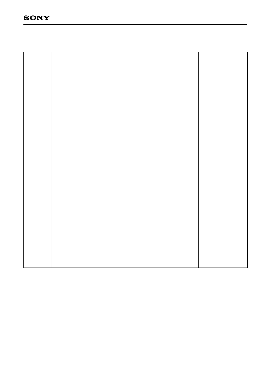
≠ 43 ≠
CXD2719Q
∑ SFC mode user setting coefficients
The relationships between the coefficient RAM and each function during SFC mode operation are as follows.
02H
03H
04H
05H
06H
07H
08H
09H
0aH
0bH
0cH
0dH
0eH
0fH
10H
11H
12H
13H
14H
15H
16H
17H
18H
19H
1aH
1bH
1cH
1dH
1eH
1fH
20H
21H
22H
23H
24H
25H
26H
k
XthP
XthM
Ksd
Ap
Am
Bp
Bm
Cp
Cm
KLsri
KRsri
Kfb
ahd
a00
a01
a02
b01
b02
KLtp0
KLtp1
KLtp2
KLtp3
KLtp4
KRtp0
KRtp1
KRtp2
KRtp3
KRtp4
KStp0
KStp1
KStp2
KStp3
b0
b1
KLdry
KRdry
Compressor gain coefficient
Compressor threshold value (+)
Compressor threshold value (≠)
Compressor ON/OFF
Compressor parameter
Compressor parameter
Compressor parameter
Compressor parameter
Compressor parameter
Compressor parameter
Delay line L-ch input volume
Delay line R-ch input volume
Delay line feedback coefficient
Feedback loop internal Hi-dump filter coefficient
Feedback loop internal LPF0 parameter
Feedback loop internal LPF0 parameter
Feedback loop internal LPF0 parameter
Feedback loop internal LPF0 parameter
Feedback loop internal LPF0 parameter
Delay line L-ch Tap0 volume
Delay line L-ch Tap1 volume
Delay line L-ch Tap2 volume
Delay line L-ch Tap3 volume
Delay line L-ch Tap4 volume
Delay line R-ch Tap0 volume
Delay line R-ch Tap1 volume
Delay line R-ch Tap2 volume
Delay line R-ch Tap3 volume
Delay line R-ch Tap4 volume
Delay line S-ch Tap0 volume
Delay line S-ch Tap1 volume
Delay line S-ch Tap2 volume
Delay line S-ch Tap3 volume
All pass filter 0 coefficient
All pass filter 1 coefficient
L-ch direct sound mix volume
R-ch direct sound mix volume
See Table 8-5-7.
See Table 8-5-7.
See Table 8-5-7.
0000 = OFF, 8000 = ON
See Table 8-5-7.
See Table 8-5-7.
See Table 8-5-7.
See Table 8-5-7.
See Table 8-5-7.
See Table 8-5-7.
See Table 8-5-5.
See Table 8-5-5.
See Tables 8-5-5, 6.
See Table 8-2-8.
See Tables 8-5-9, 10, 11.
See Tables 8-5-9, 10, 11.
See Tables 8-5-9, 10, 11.
See Tables 8-5-9, 10, 11.
See Tables 8-5-9, 10, 11.
See Tables 8-5-5, 6.
See Tables 8-5-5, 6.
See Tables 8-5-5, 6.
See Tables 8-5-5, 6.
See Tables 8-5-5, 6.
See Tables 8-5-5, 6.
See Tables 8-5-5, 6.
See Tables 8-5-5, 6.
See Tables 8-5-5, 6.
See Tables 8-5-5, 6.
See Tables 8-5-5, 6.
See Tables 8-5-5, 6.
See Tables 8-5-5, 6.
See Tables 8-5-5, 6.
See Tables 8-5-5, 6.
See Tables 8-5-5, 6.
See Table 8-5-5.
See Table 8-5-5.
Table 8-4-3 (1). SFC Mode Setting Value Coefficients
Address
Symbol
Function
Setting value
≠ 44 ≠
CXD2719Q
27H
28H
29H
2aH
2bH
2cH
2dH
2eH
2fH
30H
31H
32H
33H
34H
35H
36H
37H
5dH
81H
82H
83H
84H
85H
86H
87H
88H
89H
8aH
8bH
8cH
8dH
8eH
8fH
90H
91H
92H
93H
d6H
d9H
dcH
ddH
Address
KLeff
KReff
KLlpi
KRlpi
a10
a11
a12
b11
b12
KLlpo
KRlpo
KLod
KRod
KSod
KLd
KRd
KCod
Kd
Ltp0
Ltp1
Ltp2
Ltp3
Ltp4
Rtp0
Rtp1
Rtp2
Rtp3
Rtp4
Stp0
Stp1
Stp2
Stp3
tp_fb
ap0_in
ap0_out
ap1_in
ap1_out
KiA
Ke
Kia
Kis
Symbol
L-ch reflected sound mix volume
R-ch reflected sound mix volume
LPF1 L-ch input volume
LPF1 R-ch input volume
LPF1 parameter
LPF1 parameter
LPF1 parameter
LPF1 parameter
LPF1 parameter
LPF1 L-ch mix volume
LPF1 R-ch mix volume
L-ch output total volume
R-ch output total volume
S-ch output total volume
L-ch
C-ch mix volume
R-ch
C-ch mix volume
C-ch output total volume
Compressor input volume (both L and R)
Delay line L-ch Tap0 read address
Delay line L-ch Tap1 read address
Delay line L-ch Tap2 read address
Delay line L-ch Tap3 read address
Delay line L-ch Tap4 read address
Delay line R-ch Tap0 read address
Delay line R-ch Tap1 read address
Delay line R-ch Tap2 read address
Delay line R-ch Tap3 read address
Delay line R-ch Tap4 read address
Delay line S-ch Tap0 read address
Delay line S-ch Tap1 read address
Delay line S-ch Tap2 read address
Delay line S-ch Tap3 read address
Delay line feedback read address
All pass filter 0 delay RAM write address
All pass filter 0 delay RAM read address
All pass filter 1 delay RAM write address
All pass filter 1 delay RAM read address
Serial audio interface input volume
De-emphasis ON/OFF
Analog input mix switch
Digital input mix switch
Function
See Table 8-5-5.
See Table 8-5-5.
See Table 8-5-5.
See Table 8-5-5.
See Table 8-5-9.
See Table 8-5-9.
See Table 8-5-9.
See Table 8-5-9.
See Table 8-5-9.
See Table 8-5-5.
See Table 8-5-5.
See Table 8-5-5.
See Table 8-5-5.
See Table 8-5-5.
See Table 8-5-5.
See Table 8-5-5.
See Table 8-5-5.
See Table 8-5-5.
See Table 8-5-12.
See Table 8-5-12.
See Table 8-5-12.
See Table 8-5-12.
See Table 8-5-12.
See Table 8-5-12.
See Table 8-5-12.
See Table 8-5-12.
See Table 8-5-12.
See Table 8-5-12.
See Table 8-5-12.
See Table 8-5-12.
See Table 8-5-12.
See Table 8-5-12.
See Table 8-5-12.
See Table 8-5-12.
See Table 8-5-12.
See Table 8-5-12.
See Table 8-5-12.
See Table 8-5-5.
0000 = OFF, ac19 = ON
See Table 8-5-4.
See Table 8-5-5.
Table 8-4-3 (2). Coefficient RAM Setting Data in SFC Mode
Setting value
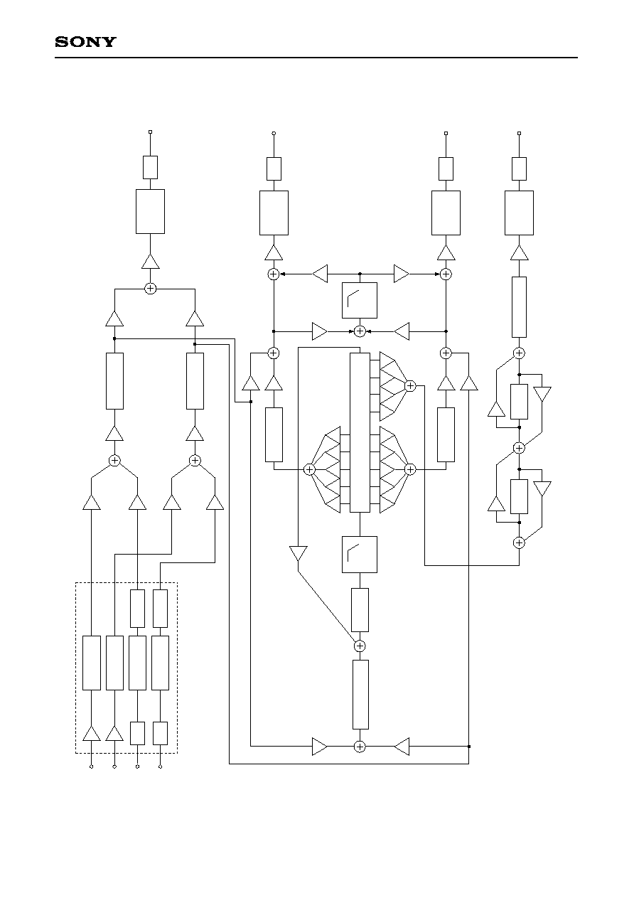
≠ 45 ≠
CXD2719Q
(2)-3. Signal Flow
A
D
C
D
e
c
i
m
a
t
i
o
n
D
C
_
C
u
t
1
A
D
C
D
e
c
i
m
a
t
i
o
n
D
C
_
C
u
t
1
D
e
E
m
p
h
a
s
i
s
L
I
N
R
I
N
S
I
A
1
S
I
A
2
D
e
E
m
p
h
a
s
i
s
≠
K
i
A
(
d
6
H
)
≠
K
i
A
(
d
6
H
)
≠
K
i
a
(
d
c
H
)
≠
K
i
s
(
d
d
H
)
≠
K
i
s
(
d
d
H
)
≠
K
i
a
(
d
c
H
)
≠
K
R
t
p
(
1
a
H
t
o
1
e
H
)
C
o
m
p
r
e
s
s
o
r
(
0
2
H
t
o
0
b
H
)
≠
K
d
(
5
d
H
)
≠
K
L
d
(
3
5
H
)
C
o
m
p
r
e
s
s
o
r
(
0
2
H
t
o
0
b
H
)
≠
K
d
(
5
d
H
)
≠
K
R
d
(
3
6
H
)
≠
K
C
o
d
(
3
7
H
)
O
v
e
r
S
a
m
p
l
i
n
g
D
A
C
X
C
O
U
T
C
-
c
h
T
h
e
s
e
t
t
i
n
g
s
f
o
r
t
h
i
s
s
e
c
t
i
o
n
a
r
e
t
h
e
s
a
m
e
a
s
f
o
r
D
P
L
m
o
d
e
.
(
S
a
m
e
c
o
e
f
f
i
c
i
e
n
t
s
a
n
d
a
d
d
r
e
s
s
e
s
)
1
2
3
0
1
2
3
4
0
1
2
3
4
0
D
e
l
a
y
(
1
0
H
t
o
1
4
H
)
S
e
c
o
n
d
a
r
y
L
P
F
L
P
F
0
H
i
D
u
m
p
≠
a
h
d
(
0
f
H
)
D
o
w
n
S
a
m
p
l
i
n
g
1
,
1
/
2
,
1
/
3
≠
K
L
e
f
f
(
2
7
H
)
H
i
-
S
a
m
p
l
i
n
g
(
2
b
H
t
o
2
f
H
)
L
P
F
1
≠
K
L
o
d
(
3
2
H
)
O
v
e
r
S
a
m
p
l
i
n
g
D
A
C
L
O
U
T
L
-
c
h
≠
K
L
d
r
y
(
2
5
H
)
≠
K
R
d
r
y
(
2
6
H
)
≠
K
R
e
f
f
(
2
8
H
)
H
i
-
S
a
m
p
l
i
n
g
≠
K
R
o
d
(
3
3
H
)
O
v
e
r
S
a
m
p
l
i
n
g
D
A
C
R
O
U
T
R
-
c
h
≠
K
f
b
(
0
e
H
)
≠
K
L
t
p
(
1
5
H
t
o
1
9
H
)
≠
K
S
t
p
(
1
f
H
t
o
2
2
H
)
≠
K
L
l
p
i
(
2
9
H
)
≠
K
L
l
p
o
(
3
0
H
)
≠
K
R
l
p
i
(
2
a
H
)
≠
K
R
l
p
o
(
3
1
H
)
≠
K
S
o
d
(
3
4
H
)
O
v
e
r
S
a
m
p
l
i
n
g
D
A
C
X
S
O
U
T
S
-
c
h
H
i
-
S
a
m
p
l
i
n
g
D
e
l
a
y
b
1
(
2
4
H
)
b
1
(
2
4
H
)
D
e
l
a
y
b
0
(
2
3
H
)
b
0
(
2
3
H
)
≠
K
R
s
r
i
(
0
d
H
)
≠
K
L
s
r
i
(
0
c
H
)
A
L
L
P
A
S
S
F
I
L
T
E
R
(
R
E
V
E
R
V
E
)
S
e
c
o
n
d
a
r
y
L
P
F
Fig. 8-4-1. Signal Flow for SFC Mode
≠ 46 ≠
CXD2719Q
8000H
c000H
e000H
eff6H
ffffH
0000H
D15 to D0
+6.02
0.00
≠6.02
≠12.00
≠84.29
≠
Level [dB]
Table 8-4-4. Kia (dcH) Setting Value Examples
8000H
a563H
c000H
d2b2H
e000H
f000H
ffffH
0000H
D15 to D0
0.00
≠3.00
≠6.02
≠9.02
≠12.04
≠18.06
≠90.31
≠
Level [dB]
Table 8-4-5. Setting Value Examples
for Each Volume
(Other than Kia, Negative Values)
7fffH
5a9dH
4000H
2d4eH
2000H
1000H
0001H
0000H
D15 to D0
0.00
≠3.00
≠6.02
≠9.02
≠12.04
≠18.06
≠90.31
≠
Level [dB]
Table 8-4-6. Setting Value Examples for Each Volume
(Other than Kia, Positive Values)
(3) Volume Settings
[Relevant data] Coefficients: KLsri (0cH), KRsri (0dH), Kfb (0eH), KLtp0 (15H), KLtp1 (16H),
KLtp2 (17H), KLtp3 (18H), KLtp4 (19H), KRtp0 (1aH), KRtp1 (1bH),
KRtp2 (1cH), KRtp3 (1dH), KRtp4 (1eH), KStp0 (1fH), KStp1 (20H),
KStp2 (21H), KStp3 (22H), b0 (23H), b1 (24H), KLdry (25H), KRdry (26H),
KLeff (27H), KReff (28H), KLlpi (29H), KRlpi (2aH), KLlpo (30H),
KRlpo (31H), KLod (32H), KRod (33H), KSod (34H), KLd (35H), KRd (36H),
KCod (37H), Kd (5dH), KiA (d6H), Kia (dcH), Kis (ddH)
The I/O levels and volumes are 2's complement format with a decimal point between D15 and D14, and
hexadecimal notation with D15 as MSB and D0 as LSB.
The coefficient and level relationships are as follows.
(3)-1. Kia (dcH): 0dB = c000H
The I/O levels for 8000H to ffffH are obtained by the following
formulas.
(Coefficient value) = [(≠1)
◊
D15 +
(Dn
◊
2
n ≠ 15
)]
◊
(≠2)
I/O level = 20 log [coefficient value] dB
(3)-2. Other Coefficients
Except for Kia, the coefficients listed in the [Relevant data] above
are basically specified by negative values (D15 to D0) with "0dB =
8000H". When intentionally inverting the phase, however, specify
positive values with "0dB = 7fffH".
The DSP calculation for coefficient values other than Kfb is
(≠1)
◊
(D15 to D0).
The I/O levels for 8000H to ffffH are obtained by the following
formulas.
(Coefficient value) = [(≠1)
◊
D15 +
(Dn
◊
2
n ≠ 15
)]
◊
(≠1)
I/O level = 20 log [coefficient value] dB
The I/O levels for 7fffH to 0001H are obtained by the following
formulas.
(Coefficient value) = [D15 +
(Dn
◊
2
n ≠ 15
)]
I/O level = 20 log [coefficient value] dB
14
n = 0
14
n = 0
14
n = 0
≠ 47 ≠
CXD2719Q
(4) Compressor
[Relevant data] Coefficients: k (02H), XthP (03H), XthM (04H), Ksd (05H), Ap (06H), Am (07H), Bp (08H),
Bm (09H), Cp (0aH), Cm (0bH)
The parameter table is shown in Table 8-4-7, and the I/O characteristics in Fig. 8-4-2.
Compressor ON: Ksd (05H) = 8000H
Compressor OFF: Ksd (05H) = 0000H
Comp_5
Comp_4
Comp_3
Comp_2
Comp_1
Threshold
XthP
Gain
k
Coefficient
Ap
Am
Bp
Bm
Cp
Cm
XthM
≠
[dB]
6.0 [dB]
0
0000
0
0000
2.0
4000
≠20 [dB]
5.2 [dB]
≠1/10
F334
1/10
0CCC
20/11
3A2E
≠17 [dB]
4.4 [dB]
≠1/7
EDB7
1/7
1249
5/3
3555
≠14 [dB]
2.9 [dB]
≠1/5
E667
1/5
1999
7/5
2CCC
≠9.5 [dB]
1.6 [dB]
≠1/3
D556
1/3
2AAA
6/5
2666
≠1.0
E000
≠100/99
DFAE
≠49/54
E2F7
≠5/8
EC00
≠9/20
F19A
1.0
2000
100/99
2052
49/54
1D09
5/8
1400
9/20
0E66
2.0
4000
200/99
40A5
52/27
3DA1
33/20
34CC
3/2
3000
2.0
4000
200/99
40A5
52/27
3DA1
33/20
34CC
3/2
3000
0
0000
≠1/99
FEB6
≠1/54
FDA2
≠1/40
FCCD
≠1/20
F99A
0
0000
1/99
014A
1/54
025E
1/40
0333
1/99
0666
Table 8-4-7. Compressor Parameter Table
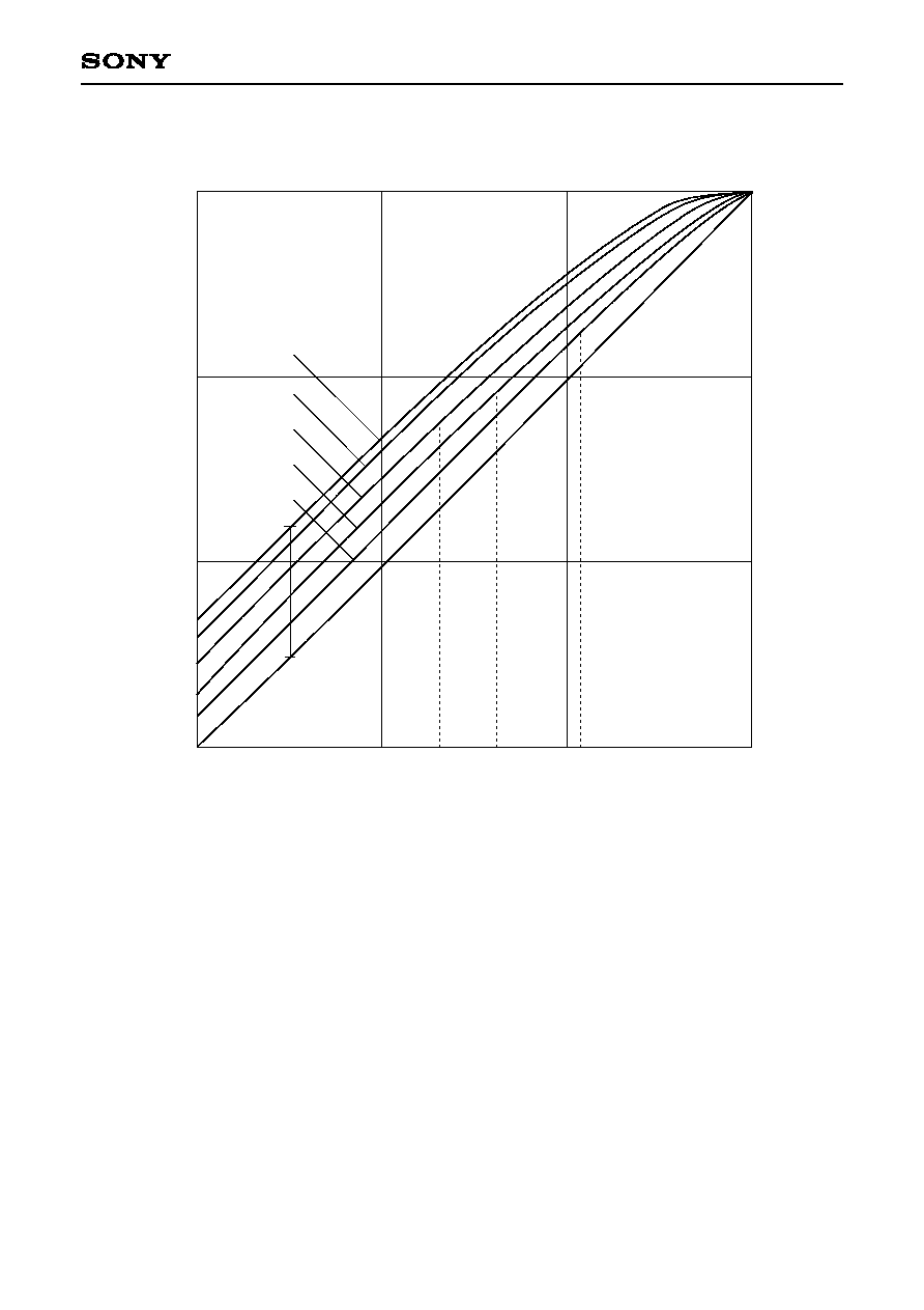
≠ 48 ≠
CXD2719Q
0
≠10
≠20
≠30
≠20
Comp4
≠17
Comp3
≠14
Comp2
≠9.5
Comp1
Threshold Level [dB]
O
u
t
p
u
t
L
e
v
e
l
[
d
B
]
≠20
≠30
≠10
Input Level [dB]
Comp5
Comp4
Comp3
Comp2
Comp1
6.0 [dB]
Linear
Fig. 8-4-2. Compressor I/O Characteristics
≠ 49 ≠
CXD2719Q
(5) Hi-Dump Filter Setting
[Relevant data] Coefficient: ahd (0fH)
This filter is used to attenuate the high frequencies. It is mainly used in the delay line feedback loop to prevent
or alleviate noise generated when high frequency components are multiplied. Table 8-4-8 shows the
parameter table.
To turn off this filter, set "ahd = 8000H".
40
60
80
100
200
400
600
800
EF46
FEEA
FE8D
FE31
FC68
F8EA
F585
F23A
1/1
1/2
1/3
FE8D
FDD5
FD1E
FC68
F8EA
F23A
EBEE
E603
FDD5
FCC3
FBB3
FAA6
F585
EBEE
E32F
DB3B
fc [Hz]
≠ahd
EF08
E073
C97A
B91E
AD94
A578
9FC6
9BCC
1/1
1/2
1/3
E073
C97A
AD94
9FC6
9912
D404
B91E
9FC6
974D
≠ahd
1k
2k
4k
6k
8k
10k
12k
14k
fc [Hz]
Table 8-4-8. Hi-Dump Filter Parameter Table
(6) Secondary LPF Settings
[Relevant data] Coefficients: a00 (10H), a01 (11H), a02 (12H), b01 (13H), b02 (14H), a10 (2bH),
a11 (2cH), a12 (2dH), b11 (2eH), b12 (2fH)
These two LPF are comprised from the same secondary IIR filters. The parameter tables are shown in Tables
8-4-9 to 8-4-11. These tables show the parameters for no decimation, 1/2 decimation and 1/3 decimation,
respectively.
Use Table 8-5-9 (No decimation) for LPF1.
The coefficients used for the LPF0 and LPF1 parameters are as follows.
LPF0: a00 (10H), a01 (11H), a02 (12H), b01 (13H), b02 (14H)
LPF1: a10 (2bH), a11 (2cH), a12 (2dH), b11 (2eH), b12 (2fH)
To turn off the filters, set only a00 and a10 to "8000H" and the other four coefficient values to "0000H".
≠ 50 ≠
CXD2719Q
5200
5300
5400
5500
5600
5700
5800
5900
6000
6100
6200
6300
6400
6500
6600
6700
6800
6900
7000
7100
7200
7300
7400
7500
7600
7700
7800
7900
8000
8100
F4A5
F448
F3EB
F38D
F32D
F2CD
F26D
F20B
F1A8
F145
F0E0
F07B
F016
EFAF
EF47
EEDF
EE76
EE0D
EDA2
ED37
ECCB
EC5E
EBF0
EB82
EB13
EAA4
EA33
E9C2
E950
E8DD
a00
a10
a01
a11
a02
a12
b01
b11
b02
b12
16B6
176F
182A
18E7
19A5
1A65
1B27
1BEA
1CB0
1D77
1E3F
1F09
1FD5
20A2
2171
2241
2313
23E7
24BC
2593
266B
2744
281F
28FC
29DA
2AB9
2B9A
2C7C
2D60
2E45
0B5B
0BB8
0C15
0C73
0CD3
0D33
0D93
0DF5
0E58
0EBB
0F20
0F85
0FEA
1051
10B9
1121
118A
11F3
125E
12C9
1335
13A2
1410
147E
14ED
155C
15CD
163E
16B0
1723
7FDF
7D90
7B43
78F7
76AD
7464
721C
6FD6
6D91
6B4D
690B
66CA
648A
624B
600D
5DD1
5B96
595C
5723
54EA
52B3
507D
4E48
4C14
49E1
47AF
457E
434D
411E
3EEF
D2B4
D391
D469
D53B
D609
D6D2
D796
D855
D910
D9C6
DA77
DB24
DBCD
DC71
DD10
DDAC
DE43
DED6
DF66
DFF0
E077
E0FA
E179
E1F4
E26C
E2DF
E34F
E3BA
E422
E487
Cut-off
frequency [Hz]
8200
8300
8400
8500
8600
8700
8800
8900
9000
9100
9200
9300
9400
9500
9600
9700
9800
9900
10000
10100
10200
10300
10400
10500
10600
10700
10800
10900
11000
OFF
E86A
E7F6
E781
E70C
E696
E61F
E5A7
E52F
E4B6
E43C
E3C1
E346
E2CA
E24D
E1D0
E152
E0D3
E053
DFD3
DF52
DED0
DE4D
DDCA
DD45
DCC0
DC3B
DBB4
DB2D
DAA5
8000
a00
a10
a01
a11
a02
a12
b01
b11
b02
b12
2F2C
3014
30FD
31E8
32D5
33C3
34B2
35A3
3695
3788
387D
3974
3A6C
3B65
3C60
3D5C
3E5A
3F5A
405A
415D
4261
4366
446D
4575
467F
478B
4898
49A6
4AB7
0000
1796
180A
187F
18F4
196A
19E1
1A59
1AD1
1B4A
1BC4
1C3F
1CBA
1D36
1DB3
1E30
1EAE
1F2D
1FAD
202D
20AE
2130
21B3
2236
22BB
2340
23C5
244C
24D3
255B
0000
3CC1
3A93
3867
363B
3410
31E5
2FBB
2D92
2B69
2941
2719
24F2
22CB
20A5
1E7F
1C5A
1A35
1810
15EB
13C7
11A3
0F7F
0D5C
0B38
0915
06F2
04CF
02AC
0089
0000
E4E8
E545
E59E
E5F4
E647
E695
E6E1
E729
E76D
E7AE
E7EC
E826
E85D
E890
E8C0
E8ED
E917
E93D
E960
E980
E99C
E9B5
E9CB
E9DD
E9ED
E9F9
EA02
EA07
EA0A
0000
Cut-off
frequency [Hz]
Table 8-4-9. Secondary LPF Parameter Table (No Decimation, Q = 0.707107)
≠ 51 ≠
CXD2719Q
2600
2700
2800
2900
3000
3100
3200
3300
3400
3500
3600
3700
3800
3900
4000
F4A5
F3EB
F32D
F26D
F1A8
F0E0
F016
EF47
EE76
EDA2
ECCB
EBF0
EB13
EA33
E950
a00
a01
a02
b01
b02
16B6
182A
19A5
1B27
1CB0
1E3F
1FD5
2171
2313
24BC
266B
281F
29DA
2B9A
2D60
0B5B
0C15
0CD3
0D93
0E58
0F20
0FEA
10B9
118A
125E
1335
1410
14ED
15CD
16B0
7FDF
7B43
76AD
721C
6D91
690B
648A
600D
5B96
5723
52B3
4E48
49E1
457E
411E
D2B4
D469
D609
D796
D910
DA77
DBCD
DD10
DE43
DF66
E077
E179
E26C
E34F
E422
Cut-off
frequency [Hz]
4100
4200
4300
4400
4500
4600
4700
4800
4900
5000
5100
5200
5300
5400
5500
OFF
E86A
E781
E696
E5A7
E4B6
E3C1
E2CA
E1D0
E0D3
DFD3
DED0
DDCA
DCC0
DBB4
DAA5
8000
a00
a01
a02
b01
b02
2F2C
30FD
32D5
34B2
3695
387D
3A6C
3C60
3E5A
405A
4261
446D
467F
4898
4AB7
0000
1796
187F
196A
1A59
1B4A
1C3F
1D36
1E30
1F2D
202D
2130
2236
2340
244C
255B
0000
3CC1
3867
3410
2FBB
2B69
2719
22CB
1E7F
1A35
15EB
11A3
0D5C
0915
04CF
0089
0000
E4E8
E59E
E647
E6E1
E76D
E7EC
E85D
E8C0
E917
E960
E99C
E9CB
E9ED
EA02
EA0A
0000
Cut-off
frequency [Hz]
Table 8-4-10. Secondary LPF Parameter Table (1/2 Decimation, Q = 0.707107)
1800
1900
2000
2100
2200
2300
2400
2500
2600
2700
2800
2900
3000
3100
3200
3300
3400
3500
3600
OFF
F3EB
F2CD
F1A8
F07B
EF47
EE0D
ECCB
EB82
EA33
E8DD
E781
E61F
E4B6
E346
E1D0
E053
DED0
DD45
DBB4
8000
a00
a01
a02
b01
b02
182A
1A65
1CB0
1F09
2171
23E7
266B
28FC
2B9A
2E45
30FD
33C3
3695
3974
3C60
3F5A
4261
4575
4898
0000
0C15
0D33
0E58
0F85
10B9
11F3
1335
147E
15CD
1723
187F
19E1
1B4A
1CBA
1E30
1FAD
2130
22BB
244C
0000
7B43
7464
6D91
66CA
600D
595C
52B3
4C14
457E
3EEF
3867
31E5
2B69
24F2
1E7F
1810
11A3
0B38
04CF
0000
D469
D6D2
D910
DB24
DD10
DED6
E077
E1F4
E34F
E487
E59E
E695
E76D
E826
E8C0
E93D
E99C
E9DD
EA02
0000
Cut-off
frequency [Hz]
Table 8-4-11. Secondary LPF Parameter Table (1/3 Decimation, Q = 0.707107)

≠ 52 ≠
CXD2719Q
(7) Delay Time Settings
[Relevant data] Coefficients: Ltp0 (81H), Ltp1 (82H), Ltp2 (83H), Ltp3 (84H), Ltp4 (85H), Rtp0 (86H),
Rtp1 (87H), Rtp2 (88H), Rtp3 (89H), Rtp4 (8aH), Stp0 (8bH), Stp1 (8cH),
Stp2 (8dH), Stp3 (8eH), tp_fb (8fH), ap0_in (90H), ap0_out (91H),
ap1_in (92H), ap1_out (93H)
Setup: SQA05, SQA04, SQC07, SQC06
First, select No decimation, 1/2 decimation or 1/3 decimation.
1/1 (No decimation): SQA11, 10 = "00", SQC07, 06 = "00"
1/2 decimation:
SQA11, 10 = "01", SQC07, 06 = "01"
1/3 decimation:
SQA11, 10 = "10", SQC07, 06 = "1
" (
= Don't care)
Next, set tp_fb (8fH) which determines the comb filter delay time, and ap0_in (90H), ap0_out (91H), ap1_in
(92H) and ap1_out (93H) which determine the all pass filter delay times.
The following conditions apply.
∑ 0
tp_fb, tp_fb + 0020H
ap0_in
ap0_out, ap0_out + 0020H
ap1_in
ap1_out
bfe0H
∑ 0
Comb filter tap (Ltp0 to Stp3)
tp_fb
Note) The minimum unit for all the above coefficients is "0020H". Values larger than this are ignored.
(7)-1. Comb Filter
First, set the comb filter maximum delay time tp_fb (8fH). The coefficient value is calculated as follows.
(Dly)
Decimal
= (Delay [s])
◊
fs [Hz]
◊
32
(The delay value is multiplied by 1/2 and 1/3 during 1/2 and 1/3 decimation, respectively.)
Next set the delay times for the comb filter taps, and calculate the coefficient values in the same manner as for
tp_fb. (0
Tap
tp_fb)
Example) For a maximum delay time of 36ms (1/2 decimation, fs = 44100Hz)
0.036
◊
(1/2)
◊
44100
◊
32 = 25401.6
Rounding up to 25402 and converting to hexadecimal notation:
633aH
However, the address is specified in 0020H increments, so this becomes:
6340H
Therefore, set all (14) of the L, R and S channel taps to 6340H (36 ms) or less. For example, the L
channel settings could be:
Ltp0 = 1ba0H (10ms)
Ltp1 = 2960H (15ms)
Ltp2 = 3720H (20ms)
Ltp3 = 44e0H (25ms)
Ltp4 = 52c0H (30ms)
Set the R and S channels in the same manner.
≠ 53 ≠
CXD2719Q
0000H
36.0ms
6340H
6360H
tp_fb
ap0_in
69.6ms (0000H to bfe0H)
9180H
ap0_out
91a0H
ap1_in
bfe0H
ap1_out
16.8ms
16.8ms
Fig. 8-4-3. Delay Time Setting Example (1/2 Decimation)
Note) Assuming the tap read address to be 0000H, the comb filter has a delay time of "0". However, the all
pass filters are delayed by one sample after reading from the delay RAM.
Therefore, perfect through operation is not possible even if (write address) = (read address).
Table 8-4-12. SFC Mode Delay Time Setting Value Examples
(7)-2. All Pass Filters (APF0, APF1)
The all pass filter delay times are determined by (read address) ≠ (write address - 0020H). Set ap
_in and
ap
_out so that this subtraction results in the target delay time setting value. The calculation method is the
same as that for tp_fb.
Example) When setting a maximum comb filter delay time of 36ms and splitting the remainder evenly
between APF0 and APF1.
(1/2 decimation)
(bfe0H ≠ 6340H)/2 = 2e50H
The address is specified in 0020H increments, so 2e40H is used for APF0, and 2e60H for APF1.
tp_fb = 6340H, so:
ap0_in = 6360H, ap0_out = 6340H + 2e40H = 9180H
ap1_in = 91a0H, ap1_out = 9180H + 2e60H = bfe0H
0020H
0040H
∑
∑
3720H
∑
6e40H
∑
a560H
∑
bf80H
bfa0H
0.022ms
0.045ms
∑
∑
10.000ms
∑
20.000ms
∑
30.000ms
∑
34.739ms
34.761ms
0.045ms
0.090ms
∑
∑
20.000ms
∑
40.000ms
∑
60.000ms
∑
69.478ms
69.523ms
0.068ms
0.136ms
∑
∑
30.000ms
∑
60.000ms
∑
90.000ms
∑
104.217ms
104.285ms
Setting
value
Delay (fs = 44.1kHz)
1/1 (No decimation)
1/2 decimation
1/3 decimation
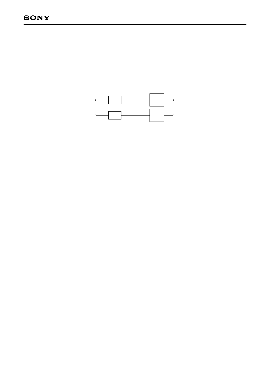
≠ 54 ≠
CXD2719Q
8-5. Bypass Mode
In this mode, the DSP is bypassed. The ADC and DAC are not used and both the L and R channels are in
analog-to-analog through status.
(1) Setting Bypass Mode
Set the uppermost bit (SQA15) of setup register Field A to "1".
The other setup data and coefficient data is "Don't care".
MUX &
LPF
LPF
LIN
LOUT
MUX &
LPF
LPF
RIN
ROUT
Fig. 8-5-1. Bypass Mode
In bypass mode, the output after ADC prefilter and the output after DAC postfilter are swtiched by the analog
switch. The popping noise occurs at switching due to the difference of these filter's reference voltages
(500mV). Therefore, the countermeasure against the noise, such as the system muting, is required when using
this mode.
≠ 55 ≠
CXD2719Q
Appendix 1. Soft Mute
The condition where the final volume coefficient data connected to the CXD2719Q output of each mode is off
(= 0000H) is called "soft mute".
(Soft mute cannot be applied in bypass mode.)
Table 9 shows the coefficients that should be set to 0000H in each mode during soft mute. Table 9 also
includes the loop input volume coefficients and feedback volume coefficients for modes which contain a
feedback loop.
KLV (00), KRV (01), KCV (02), KSV (03), KLd (0e), KRd (0f), KCd (10), KSd (11),
Kfb (12), KDV1 (21), KDV2 (22), KDV3 (23), KLRm1 (24), KLRm2 (25), KLRm3 (26),
KL (f2), KR (f3), KH (f4), KP (f5), KCH (f6), KCP (f7), KS (f8)
Same as Pro Logic mode
Same as Pro Logic or Virtual mode
KLsri (0c), KRsri (0d), Kfb (0e), KLod (32), KRod (33), KSod (34), KCod (37)
Pro Logic mode
Dolby 3 Stereo mode
Noise sequencer mode
SFC mode
Mode name
Coefficient name (Address [H])
Table 9. Recommended Mute Coefficients
RAM Initialization
Although this LSI contains a number of RAM, there is no clear function and the like. Therefore, it is impossible
to predict the type of data existing in the RAM after power-on. Also, the previous mode's data remains even
after the mode is changed, possibly causing momentary noise. If these problems cannot be handled by the
system mute, apply soft mute for a time equal to the maximum delay time of the delay RAM (varies according
to the mode and coefficient settings) during power-on and when changing the mode. This clears all the RAM.
Example 1)
When using 20.0ms for the passive decoder and 14.8ms for the simple SFC delay line
The maximum delay time is 20.0ms, so soft mute must be applied continuously for 20.0ms.
Example 2)
When using the delay RAM in SFC mode with 1/2 decimation
Comb filter delay time = 36.0ms
All pass filter delay time = 16.8ms
The maximum delay time is 36.0ms, so soft mute must be applied for 36.0ms.
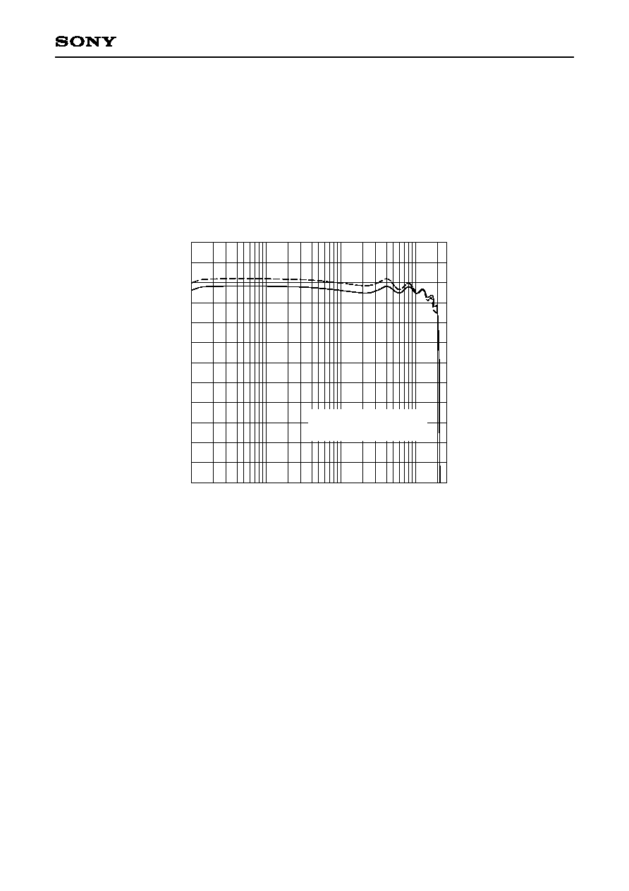
≠ 56 ≠
CXD2719Q
Appendix 2. Compensation Filter
This filter compensates the shoulder characteristics of the digital filters. Fig. 9 shows the frequency response
measured under the following conditions.
∑ Vin = 300mVrms (sine wave)
∑ Output level at 1kHz = 0dB
∑ DC cut filter cut-off = 5kHz
+2
+1
0
≠1
≠2
≠3
≠4
≠5
≠6
≠7
≠8
≠9
≠10
20
10
100
50
200
500
2k
1k
5k
10k
20k
Frequency [Hz]
L
e
v
e
l
[
d
B
]
Hosho filter [L-ch]
0dB = 300mVrms (1kHz sin)
Fig. 9. Compensation Filter Frequency Response (Dotted line: Without the compensation filter)
Operation
Turn the filter on and off in each mode except bypass mode using SQA12 of setup register Field A. See "6.
Setup Register".
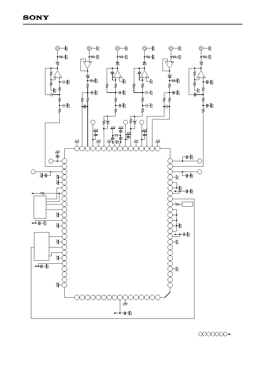
≠ 57 ≠
CXD2719Q
Application Circuit
T.P
T.P
T.P
T.P
V
SS
0
T.P
T.P
T.P
TS
T0
V
DD
0
V
SS
1
TS
T1
TS
T2
TS
T3
TS
T4
XR
ST
BF
OT
CS
L1
CS
L2
V
SS
2
AV
S3
AV
D3
LO
UT
AV
D1A
V
S
1
L
O
1
L
I
N
A
V
D
5
A
V
S
5
X
C
O
U
T
A
V
D
X
X
T
L
O
X
T
L
I
A
V
S
X
X
S
O
U
T
A
V
S
6
A
V
D
6
R
I
N
L
O
2
A
V
S
2
V
SS
6
T.P
T.P
T.P
BC
K
T.P
SI
T.P
V
SS
4
V
DD
1
XS
24
RV
DT
T.P
RE
DY
SC
K
V
SS
3
AV
S4
AV
D4
RO
UT
AV
D2
XL
AT
V
SS
5
LR
CK
XM
ST
T
.
P
T
.
P
T
.
P
T
.
P
T
.
P
T
.
P
V
S
S
7
V
D
D
2
T
.
P
T
.
P
T
.
P
T
.
P
T
.
P
T
.
P
T
.
P
T
.
P
G
A
G
N
D
A
G
N
D
0
.
1
µ
D
G
N
D 0.
1
µ
D
G
N
D
XR
ST
D
G
N
D
D
G
N
D
D
G
N
D
D
G
N
D
D
G
N
D
D
G
N
D
D
G
N
D
D
G
N
D
D
G
N
D
D
G
N
D
D
G
N
D
A
G
N
D
A
A
G
N
D
0
.
1
µ
M
i
c
r
o
c
o
m
p
u
t
e
r
0
.
1
µ
0
.
1
µ
D
G
N
D
D
G
N
D
L
R
C
K
D
A
1
5
D
A
1
6
C
X
D
2
5
0
0
A
Q
X
T
A
I
A
G
N
D
2
2
p
A
G
N
D
A
G
N
D
A
G
N
D
A
G
N
D
1
0
µ
1
0
0
k
C
A
G
N
D
0
.
1
µ
B
0
.
1
µ
A
G
N
D
1
.
2
k
2
2
0
0
p
5
.
6
k
2
2
0
0
p
8
.
2
k
A
G
N
D
A
G
N
D
A
G
N
D
4
7
k
1
0
0
p
1
0
µ
A
G
N
D
S
o
u
t
A
G
N
D
1
0
0
k
A
G
N
D
2
2
k
1
5
k
1
0
0
p
3
3
k
1
0
µ
A
G
N
D
1
M
R
i
n
A
G
N
D
A
G
N
D
D
0
.
1
µ
1
0
µ
1
0
0
k
1
.
2
k
1
0
0
0
p
5
.
6
k
1
0
0
0
p
8
.
2
k
A
G
N
D
A
G
N
D
A
G
N
D
4
7
k
4
7
p
1
0
µ
A
G
N
D
A
G
N
D
1
0
0
k
A
G
N
D
1
5
k
2
2
k
3
3
k
1
0
µ
A
G
N
D
1
M
A
G
N
D
A
G
N
D
3
.
3
k
1
0
0
0
p
1
0
k
1
0
k
A
G
N
D
A
G
N
D
1
0
k
1
0
µ
A
G
N
D
A
G
N
D
1
0
0
k
A
B
C
D
E
F
G
I
C
2
I
C
2
I
C
3
I
C
3
I
C
1
1
0
0
k
1
0
0
k
3
3
0
p
3
3
0
p
1
2
k
A
G
N
D
3
3
0
p
A
G
N
D
0
.
1
µ
F
E
0
.
1
µ
A
G
N
D
A
G
N
D
1
4
5
6
7
8
9
1
0
2
3
1
1
1
2
1
3
1
4
1
5
1
6
1
7
1
8
1
9
2
0
2
1
2
2
2
3
2
4
2
5
2
6
2
7
2
8
2
9
3
0
3
1
3
4
3
5
3
6
3
7
3
8
3
9
4
0
6
5
6
6
6
7
6
8
6
9
7
0
7
1
7
2
7
3
7
4
7
5
7
6
7
7
7
8
7
9
8
0
4
1
4
2
4
3
4
4
4
5
4
6
4
7
4
8
4
9
5
0
5
1
5
2
5
3
5
4
5
5
5
6
5
7
5
8
5
9
6
0
6
1
6
3
6
4
6
2
C
o
u
t
L
i
n
L
o
u
t
3
.
3
k
1
0
0
0
p
1
0
k
1
0
k
A
G
N
D
A
G
N
D
1
0
k
1
0
µ
A
G
N
D
A
G
N
D
1
0
0
k
I
C
1
1
2
k
A
G
N
D
3
3
0
p
R
o
u
t
3
3
0
p
3
3
0
p
1
0
0
p
0
.
1
µ
0
.
1
µ
D
G
N
D
A
G
N
D
A
G
N
D
1
0
0
0
0
p
C
X
D
2
7
1
9
Q
3
2
3
3
2
2
p
4
.
7
µ
:
R
O
U
T
+
5
V
p
o
w
e
r
s
u
p
p
l
y
:
R
I
N
+
5
V
p
o
w
e
r
s
u
p
p
l
y
:
X
S
O
U
T
+
5
V
p
o
w
e
r
s
u
p
p
l
y
:
C
r
y
s
t
a
l
o
s
c
i
l
l
a
t
o
r
c
i
r
c
u
i
t
+
5
V
p
o
w
e
r
s
u
p
p
l
y
:
X
C
O
U
T
+
5
V
p
o
w
e
r
s
u
p
p
l
y
:
L
I
N
+
5
V
p
o
w
e
r
s
u
p
p
l
y
:
L
O
U
T
+
5
V
p
o
w
e
r
s
u
p
p
l
y
N
E
5
5
2
2
,
c
o
n
t
a
i
n
i
n
g
2
a
m
p
l
i
f
i
e
r
s
,
a
r
e
u
s
e
d
f
o
r
o
p
e
r
a
t
i
o
n
a
l
a
m
p
l
i
f
i
e
r
s
.
T
a
k
e
c
a
r
e
f
o
r
t
h
e
i
r
c
o
m
b
i
n
a
t
i
o
n
s
.
U
s
e
±
1
2
V
p
o
w
e
r
s
u
p
p
l
i
e
s
f
o
r
t
h
e
o
p
e
r
a
t
i
o
n
a
l
a
m
p
l
i
f
i
e
r
s
a
n
d
c
o
n
n
e
c
t
0
.
1
µ
F
b
y
p
a
s
s
c
a
p
a
c
i
t
o
r
s
.
U
s
e
D
a
i
s
h
i
n
k
u
(
A
T
-
4
9
,
3
3
.
8
6
8
8
M
H
z
)
f
o
r
t
h
e
c
r
y
s
t
a
l
o
s
c
i
l
l
a
t
o
r
.
W
i
r
i
n
g
i
n
d
i
c
a
t
e
d
b
y
b
o
l
d
l
i
n
e
s
s
h
o
u
l
d
b
e
(
1
)
t
h
i
c
k
,
(
2
)
s
h
o
r
t
,
a
n
d
(
3
)
s
h
i
e
l
d
e
d
a
r
o
u
n
d
i
t
s
p
e
r
i
p
h
e
r
y
b
y
G
N
D
.
R
e
s
i
s
t
o
r
d
e
v
i
a
t
i
o
n
:
±
1
%
,
c
a
p
a
c
i
t
o
r
d
e
v
i
a
t
i
o
n
:
±
5
%
(
E
s
p
e
c
i
a
l
l
y
,
t
h
e
d
e
v
i
a
t
i
o
n
o
f
t
h
e
A
/
D
c
o
n
v
e
r
t
e
r
f
r
o
n
t
-
s
t
a
g
e
r
e
s
i
s
t
o
r
h
a
s
a
b
a
d
i
n
f
l
u
e
n
c
e
o
n
t
h
e
s
e
p
a
r
a
t
i
o
n
w
h
e
n
u
s
i
n
g
P
r
o
L
o
g
i
c
)
T
h
e
p
h
a
s
e
s
o
f
t
h
e
c
e
n
t
e
r
a
n
d
s
u
r
r
o
u
n
d
c
h
a
n
n
e
l
s
a
r
e
i
n
v
e
r
t
e
d
a
n
d
o
u
t
p
u
t
.
T
h
e
r
e
f
o
r
e
,
b
e
s
u
r
e
t
o
i
n
v
e
r
t
t
h
e
m
b
y
t
h
e
e
x
t
e
r
n
a
l
a
m
p
l
i
f
i
e
r
.
:
D
i
g
i
t
a
l
+
5
V
p
o
w
e
r
s
u
p
p
l
y
Application circuits shown are typical examples illustrating the operation of the devices. Sony cannot assume responsibility fo
r
any problems arising out of the use of these circuits or for any infringement of third party patent and other right due to same
.
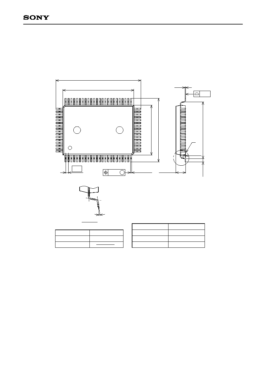
≠ 58 ≠
CXD2719Q
Package Outline
Unit: mm
PACKAGE STRUCTURE
SONY CODE
EIAJ CODE
JEDEC CODE
QFP-80P-L01
QFP080-P-1420
PACKAGE MATERIAL
LEAD TREATMENT
LEAD MATERIAL
PACKAGE MASS
EPOXY RESIN
SOLDER PLATING
42/COPPER ALLOY
1.6g
23.9 ± 0.4
20.0 ≠ 0.1
+ 0.4
1
80
65
64
41
40
25
24
0.8
0.35 ≠ 0.1
+ 0.15
1
4
.
0
≠
0
.
1
+
0
.
4
1
7
.
9
±
0
.
4
1
6
.
3
0.1 ≠ 0.05
+ 0.2
2.75 ≠ 0.15
+ 0.35
0
.
8
±
0
.
2
0.15 ≠ 0.05
+ 0.1
80PIN QFP (PLASTIC)
M
0.2
0.15
0∞ to 10∞
DETAIL A
A