
≠ 1 ≠
CXD2951GA-2
176 pin LFLGA (Plastic)
Single Chip GPS LSI
Description
The CXD2951GA-2 is a dedicated single chip LSI
for the GPS (Global Positioning System), satellite-
based location measurement system. This LSI
enables the configuration of a single chip system
providing a cost-effective, low-power solution.
Compared with conventional methods, position
detection time and sensitivity are substantially
improved with the use of an advanced signal
processing scheme. With the integration of both the
Radio and baseband blocks into a single CMOS IC,
the CXD2951GA-2 is ideal for use in automotive,
cellular handset, handheld navigation, mobile
computing and other location-based applications.
Features
∑ 12-channel GPS receiver capable of simultaneously
receiving 12 satellites
∑ Reception frequency: 1575.42MHz
(L1 band, CA code)
∑ Reference clock (TCXO) frequency:
18.414MHz (GPS, Sony standard),
The unique frequency of major applications is available,
such as GSM and W-CDMA. (optional)
13.000MHz (GSM),
14.400MHz (CDMA),
16.368MHz (GPS),
19.800MHz (PDC/CDMA),
26.000MHz (GSM)
∑ 32 bits RISC CPU (ARM7TDMI)
∑ 288K-bytes Program ROM
∑ 72K-bytes Data RAM
Power is supplied only to 8K-byte Data RAM while
in backup mode.
∑ System power management
∑ 1-channel UART
∑ Internal RTC (Real Time Clock)
∑ 10-bit successive approximation system A/D
converter, A/D data available on NMEA messages
∑ All-in-view positioning
∑ Communication format: Supports NMEA-0183
∑ 1 PPS output
∑ Supports assisted-GPS for cellular (optional)
Radio
∑ Image Rejection Mixer
∑ VCO Tank
∑ IF Filters
Structure
Silicon gate CMOS IC
Absolute Maximum Ratings
∑ Supply voltage I/O
IOV
DD
≠0.5 to +4.6
V
∑ Supply voltage core
CV
DD
≠0.5 to +2.5
V
∑ Supply voltage radio
V
DD
≠0.5 to +2.5
V
∑ Input voltage
V
I
≠0.5 to +6
V
∑ Output voltage
V
O
≠0.5 to +6
V
∑ Operating temperature Topr
≠40 to +85
∞C
∑ Storage temperature
Tstg
≠50 to +150
∞C
Recommended Operating Conditions
∑ Supply voltage I/O
IOV
DD
3.0 to 3.6
V
Under operation with internal ROM, using no
external expansion bus:
IOV
DD
2.6 to 3.6
V
Under operation in backup mode:
BKUPIOV
DD
2.5 (Min.) V
∑ Supply voltage core
CV
DD
1.62 to 1.98
V
∑ Supply voltage radio
V
DD
1.62 to 1.98
V
∑ Operating temperature Topr
≠40 to +85
∞C
Input/Output Pin Capacitance (Baseband)
∑ Input capacitance
C
IN
9 (Max.)
pF
∑ Output capacitance
C
OUT
11 (Max.)
pF
∑ I/O capacitance
C
I/O
11 (Max.)
pF
E04445A49
Sony reserves the right to change products and specifications without prior notice. This information does not convey any license by
any implication or otherwise under any patents or other right. Application circuits shown, if any, are typical examples illustrating the
operation of the devices. Sony cannot assume responsibility for any problems arising out of the use of these circuits.

≠ 2 ≠
CXD2951GA-2
Performance
Baseband
∑ Tracking sensitivity:
≠152dBm (average) or less
∑ Acquisition sensitivity: ≠139dBm (average) or less in Normal mode
≠150dBm (average) or less in High sensitivity mode
Reference data using the Sony's reference board when using both an antenna of 0dBi and a RF amplifier
with NF
2dB, 25dB gain.
∑ TTFF (Time to First Fix):
Time until initial position measurement after power-on with the following conditions:
Cold Start (without both ephemeris and almanac time): 50s (average) / 60s (95% possibility)
Warm Start (without ephemeris but with almanac time): 35s (average) / 40s (95% possibility)
Hot Start (with both ephemeris and almanac time): 2s (minimum) / 6s (95% possibility)
Reference data with elevation angle of 5∞ or more and no interception environment with satellite powers
≠130dBm. (Not in High sensitivity mode)
Note) "95% possibility" means "position time with 95% possibility".
∑ Positioning accuracy:
2DRMS: approx. 5m
Reference data with elevation angle of 5∞ or more and no interception environment with satellite powers
≠130dBm.
∑ Measurement data update time: 1s
∑ Power consumption:
50mW (average) while position calculating with tracking satellites in low power mode
120mW (average) while position calculating with acquiring and tracking satellites
Reference data using the Sony's reference board when the reference clock input is 18.414MHz, and its
amplitude is 3.3V swing.
∑ 1PPS output
1µs or less precision, 1PPS outputs from ECLKOUT (Pin 97).
Note) These values are not guaranteed, depending on the conditions.
Radio
∑ Total Gain (typ.):
100dB
∑ Noise figure (typ.):
8dB
∑ Synthesizer phase noise (typ.):
≠70dBc/Hz (10kHz)
≠80dBc/Hz (100kHz)
∑ PLL spurious (typ.):
≠45dBc (inside fosc ±1.023MHz)
≠55dBc (outside fosc ±1.023MHz)
Note) These values are not guaranteed.
≠ 3 ≠
CXD2951GA-2
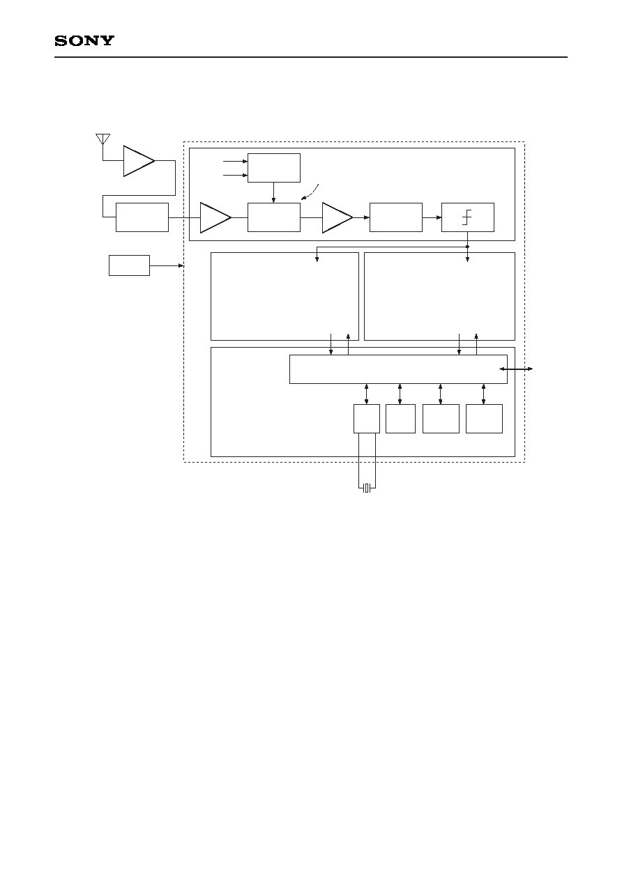
System Block Diagram
ROM
288KB
RAM
72KB
Timer
3ch
ARM7TDMI
Costas Loop & DLL
1 bit
LPF
BPF
Down
Converter
Freq.
Synthesizer
TCXO
CPU
LNA
SAW
Reference clock
18.414MHz
(GPS, Sony standard)
TCXO
LNA
1575.42MHz
1.023MHz
RF/IF
1575.42MHz
1.023MHz
Computation
& Control
∑ Control Acquisition
&
Tracking block
∑ Position calculating
Acquisition Block
∑ Acquire GPS signals
Tracking Block
∑ Locking to GPS signals
∑ 12ch correlations
RTC
I/O
UART
A/D
X'tal
32.768kHz
≠ 4 ≠
CXD2951GA-2
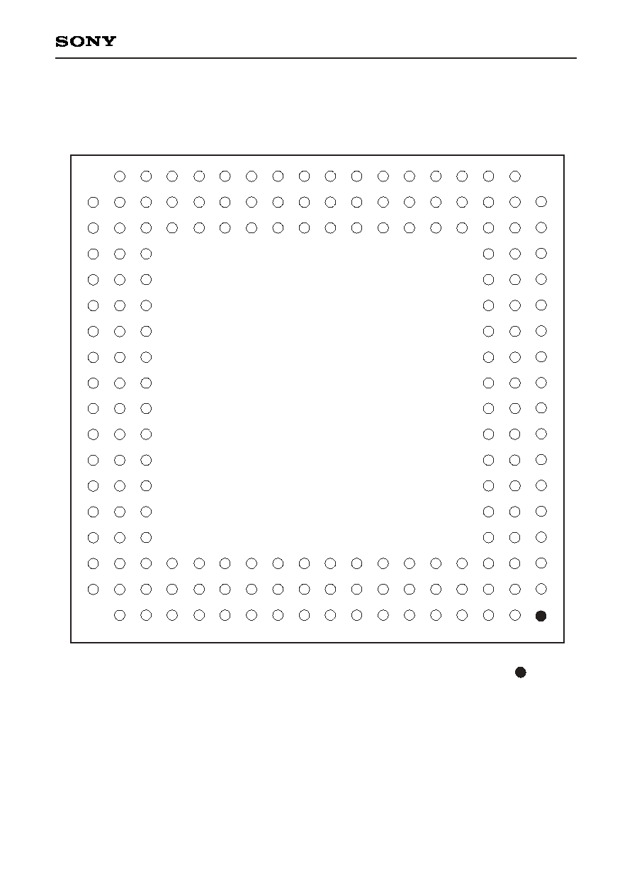
Pin Configuration (Top View)
6
3
176
81
83
82
137
135
140
85
86
84
96
98
100
103
105
107
122
125
127
129
133
136
62
60
61
161
157
156
64
63
65
158
154
153
76
77
74
143
141
144
79
80
78
139
138
142
53
48
55
169
164
166
57
54
52
167
163
162
59
56
58
165
159
160
71
70
69
147
149
151
75
73
72
145
146
148
67
68
66
155
150
152
50
46
51
173
171
168
47
44
43
39
35
32
28
24
21
9
174
172
90
92
93
94
102
104
106
110
118
120
126
128
130
87
88
89
91
95
97
99
101
108
121
123
124
131
132
134
49
45
40
37
33
31
27
29
25
11
7
5
1
175
170
42
41
38
36
34
30
26
22
14
10
8
15
12
111
113
119
19
112
115
116
109
114
117
23
20
13
18
17
16
4
2
EA3
EA5
CV
SS
3
EA9
IOV
DD
2
ETEST0
CV
SS
2
IF2GND IF1GND
TEST
OUTP
MIXGND LNASRC
RFIN
18
17
16
15
14
13
9
8
7
6
5
4
3
2
1
V
U
T
R
P
N
M
L
K
J
H
G
F
E
D
C
B
A
V
U
T
R
P
N
M
L
K
J
H
G
F
E
D
C
B
A
EA0
EA2
EA4
EA7
EA8
EA11
CV
DD
2
VCOM
IF1V
CC
TEST
OUTN
MIXGND MIXGND LNASRC MIXGND NRING
CV
DD
4
EA1
EA6
CV
DD
3
EA10
EA12
ETEST1
RREF
IF2V
CC
TESTINN
TEST
OUTD
TESTINP RFSUB RFRREF LNAMAT
ECLKI
CV
SS
4
IOV
DD
3
V
DD
VCO VCODE
CAP
V
SS
VCO
ECLKO
IOV
SS
3
EXROMI
V
DD
CP
LPFRF
V
SS
CP
EADVRB ECLKOUT EAVDPLL
V
DD
PLL V
SS
PLL
LPFIF
EVIN1 EAVSPLL
EVIN0
ETESTTCK TMS RADIOSUB
EVIN3 EAVSAD
EVIN2
ETESTTMS TDI
TCK
ETEST3 EAVDAD EADVRT
ETESTTDI ETESTTINT TDO
BKUPIOV
DD
ECLKS1 ECLKS2
EPORT10
EPORT8 IOV
SS
1
ECLKS0 IOV
SS
4
EXCS1
EPORT6
EPORT5 EPORT9
EXOE
EXCS0
EXWE3
EPORT4
EPORT2 EPORT7
IOV
DD
7
IOV
SS
8
ETEST4
ETESTTDO
CV
DD
1
CV
SS
1
ECCKI BKUPCV
DD
BKUPCV
SS
TRST
IOV
DD
1 EXTCXO
ECCKO BKUPIOV
SS
EOSCEN
EPORT12 EPORT11 ETCXO
EXWE2
IOV
SS
5
EXWE1
ED27
ED25
ED21
ED12
ED9
ED5
ED3
ED1
ERXD0 EPORT0 IOV
DD
6 EPORT3
EXWE0
IOV
DD
4
ED31
ED29
ED26
ED23
IOV
DD
5
ED13
ED11
ED7
ED6
CV
SS
6
IOV
SS
7
ETXD0 EPORT1
ED30
ED28
ED24
ED22
ED20
IOV
SS
6
ED14
ED10
IOV
SS
2
EA15
EA19
12
11
10
18
17
16
15
14
13
9
8
7
6
5
4
3
2
1
12
11
10
EA13
EA16
EA18
EA14
EA17
ETEST2
ED19
ED17
ED15
ED18
CV
SS
5
CV
DD
5
ED16
EXRS ETESTXRS
ED8
ED4
ED2
ED0
CV
DD
6
: Pin 1 index.

≠ 5 ≠
CXD2951GA-2
Pin Description
Pin
No.
1
2
3
4
5
6
7
8
9
10
11
12
13
14
15
16
17
18
19
20
21
22
23
24
25
26
27
28
Symbol
EPORT0
EPORT1
EPORT2
EPORT3
EPORT4
EPORT5
EPORT6
EPORT7
EPORT8
EPORT9
EPORT10
EPORT11
EPORT12
IOV
SS
1
IOV
DD
1
ETCXO
EXTCXO
CV
SS
1
CV
DD
1
TRST
ETESTTINT
TDO
ETESTTDO
TDI
ETESTTDI
TCK
ETESTTCK
TMS
I/O
I/O/Z
I/O/Z
I/O/Z
I/O/Z
I/O/Z
I/O/Z
I/O/Z
I/O/Z
I/O/Z
I/O/Z
I/O/Z
I/O/Z
I/O/Z
I
O
I
O
O
O
I
I
I
I
I
Description
I/O port 0
(with a software controllable pull-down resistor, Connected to GND with a resistor.)
I/O port 1
(with a software controllable pull-down resistor, See software application note.)
I/O port 2
(with a software controllable pull-down resistor, See software application note.)
I/O port 3
(with a software controllable pull-down resistor, See software application note.)
I/O port 4
(with a software controllable pull-down resistor, See software application note.)
I/O port 5
(with a software controllable pull-down resistor, See software application note.)
I/O port 6
(with a software controllable pull-down resistor, See software application note.)
I/O port 7
(with a software controllable pull-down resistor, See software application note.)
I/O port 8
(with a software controllable pull-down resistor, See software application note.)
I/O port 9
(with a software controllable pull-down resistor, See software application note.)
I/O port 10
(with a software controllable pull-down resistor, See software application note.)
I/O port 11
(with a software controllable pull-down resistor, See software application note.)
I/O port 12
(with a software controllable pull-down resistor, See software application note.)
GND
3.3V
TCXO oscillator (Frequency selectable, See software application note.)
GND
1.8V
Test (Open, with a pull-down resistor)
Test
Test
Test
Test (Open, with a pull-up resistor)
Test (Open, with a pull-up resistor)
Test (Open, with a pull-down resistor)
Test (Open, with a pull-down resistor)
Test (Open, with a pull-up resistor)