- 1 -
E05313-PS
Sony reserves the right to change products and specifications without prior notice. This information does not convey any license
by any implication or otherwise under any patents or other right. Application circuits shown, if any, are typical examples illustrating
the operation of the devices. Sony cannot assume responsibility for any problems arising out of the use of these circuits.
CXD2951GL-4
Single Chip GPS LSI
Description
The CXD2951GL-4 is a dedicated single chip LSI for the GPS (Global Positioning System), satellite-based
location measurement system. This LSI enables the configuration of a single chip system providing a cost-
effective, low-power solution.
Compared with conventional methods, position detection time and sensitivity are substantially improved with
the use of an advanced signal processing scheme. With the integration of both the Radio and baseband blocks
into a single CMOS IC, the CXD2951GL-4 is ideal for use in automotive, cellular handset, handheld navigation,
mobile computing and other location-based applications.
Features
WAAS support
12-channel GPS receiver capable of simultaneously receiving 12 satellites
Reception frequency: 1575.42MHz (L1 band, CA code)
Reference clock (TCXO) frequency: 18.414MHz (GPS, Sony standard),
The unique frequency of major applications is available, such as GSM and W-CDMA. (optional)
13.000MHz (GSM),
14.400MHz (CDMA),
16.368MHz (GPS),
19.800MHz (PDC/CDMA),
26.000MHz (GSM)
32 bits RISC CPU (ARM7TDMI)
288K-bytes Program ROM
72K-bytes Data RAM
Power is supplied only to 8K-byte Data RAM while in backup mode.
System power management
1-channel UART
Internal RTC (Real Time Clock)
10-bit successive approximation system A/D converter
All-in-view positioning
Communication format: Supports NMEA-0183 (Ver 3.01)
1PPS output
<
RADIO
>
Image Rejection Mixer
VCO Tank
IF Filters

CXD2951GL-4
- 2 -
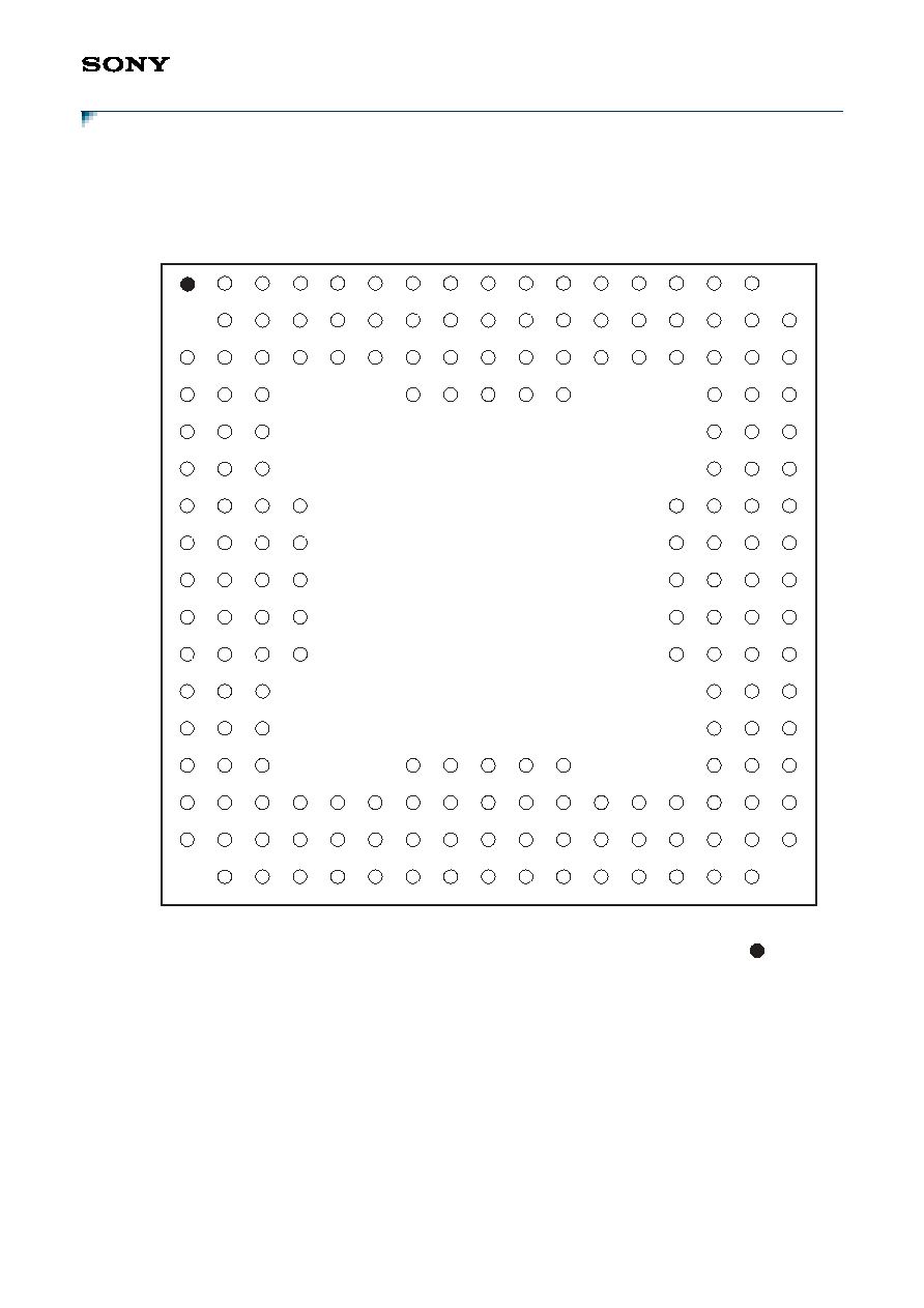
Package
183 pin VFLGA (Plastic)
Structure
Silicon gate CMOS IC
Absolute Maximum Ratings
Recommended Operating Conditions
Input/Output Pin Capacitance (Baseband)
Supply voltage I/O
IOV
DD
�0.5 to +4.6
V
Supply voltage core
CV
DD
�0.5 to +2.5
V
Supply voltage radio
V
DD
�0.5 to +2.5
V
Input voltage
V
I
�0.5 to +6
V
Output voltage
V
O
�0.5 to +6
V
Operating temperature
Topr
�40 to +85
�
C
Storage temperature
Tstg
�50 to +150
�
C
Supply voltage I/O
IOV
DD
3.0 to 3.6
V
*
Under operation with internal ROM, using no external expansion bus:
IOV
DD
2.6 to 3.6
V
*
Under operation in backup mode:
BKUPIOV
DD
2.5 (Min.)
V
Supply voltage core
CV
DD
1.62 to 1.98
V
Supply voltage radio
V
DD
1.62 to 1.98
V
Operating temperature
Topr
�40 to +85
�
C
Input pin capacitance
C
IN
9 (Max.)
pF
Output pin capacitance C
OUT
11 (Max.)
pF
I/O pin capacitance
C
I/O
11 (Max.)
pF

CXD2951GL-4
- 3 -
Performance
Baseband
Tracking sensitivity: �152dBm (average) or less
Acquisition sensitivity: �139dBm (average) or less in Normal mode
*
Reference data using the Sony's reference board when using both an antenna of 0dBi and a RF amplifier
with NF
2dB, 25dB gain.
TTFF (Time to First Fix):
Time until initial position measurement after power-on with the following conditions:
Cold Start (without both ephemeris and almanac time): 40s (average) / 50s (95% possibility)
Warm Start (without ephemeris but with almanac time): 33s (average) / 40s (95% possibility)
Hot Start (with both ephemeris and almanac time): 2s (minimum) / 3s (95% possibility)
*
Reference data with elevation angle of 5
�
or more and no interception environment with satellite powers
�130dBm.
Note) "95% possibility" means "position time with 95% possibility".
Positioning accuracy:
2DRMS: approx. 2m
*
Reference data with elevation angle of 5
�
or more and no interception environment with satellite powers
30dBm.
Measurement data update time: 1s
Power consumption:
50mW (average) while position calculating with tracking satellites in low power mode
120mW (average) while position calculating with acquiring and tracking satellites
*
Reference data using the Sony's reference board when the reference clock input is 18.414MHz, and its
amplitude is 3.3V swing.
1PPS output
1
�
s or less precision, 1PPS outputs from ECLKOUT (Pin 97).
Note) These values are not guaranteed, depending on the conditions.
Radio
Total Gain (typ.):
100dB
Noise figure (typ.):
8dB
Synthesizer phase noise (typ.):
�70dBc/Hz (10kHz)
�80dBc/Hz (100kHz)
PLL spurious (typ.):
�45dBc (inside fosc
�
1.023MHz)
�55dBc (outside fosc
�
1.023MHz)
Note) These values are not guaranteed.