CXD3029R
Description
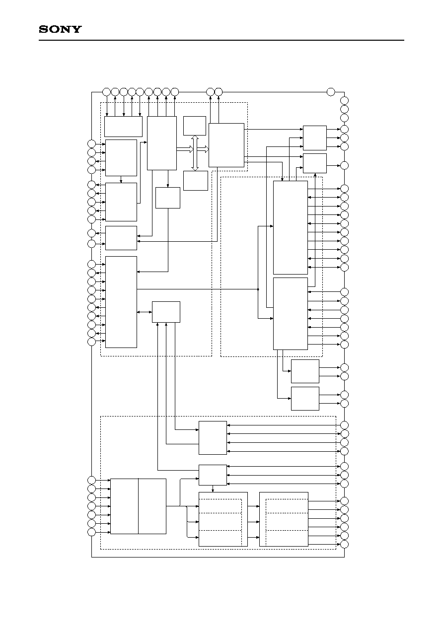
The CXD3029R is a digital signal processor LSI for CD
players. This LSI incorporates a digital servo, high & bass
boost, shock-proof memory controller, 1-bit DAC and
analog low-pass filter.
Features
· All digital signal processing during playback is performed
with a single chip
· Highly integrated mounting possible due to a built-in RAM
Digital Signal Processor (DSP) Block
· Supports CAV (Constant Angular Velocity) playback
· Frame jitter free
· 0.5
×
to 4
×
speed continuous playback possible
· Allows relative rotational velocity readout
· Wide capture range playback mode
· Spindle rotational velocity following method
· Supports 1
×
to 4
×
speed playback
· Supports variable pitch playback
· The bit clock, which strobes the EFM signal, is generated
by the digital PLL.
· EFM data demodulation
· Enhanced EFM frame sync signal protection
· Refined super strategy-based powerful error correction
C1: double correction, C2: quadruple correction
Supported during 4
×
speed playback
· Noise reduction during track jumps
· Auto zero-cross mute
· Subcode demodulation and subcode-Q data error
detection
· Digital spindle servo
· 16-bit traverse counter
· Asymmetry correction circuit
· CPU interface on serial bus
· Error correction monitor signal, etc. output from a new
CPU interface
· Servo auto sequencer
· Fine search performs track jumps with high accuracy
· Digital audio interface outputs
· Digital level meter, peak meter
· Bilingual compatible
· VCO control mode
· CD TEXT data demodulation
· Digital Out can be generated from the audio serial input.
(also supported after shock-proof and digital bass boost
processing, subcode-Q addition function)
Digital Servo (DSSP) Block
· Microcomputer software-based flexible servo control
· Offset cancel function for servo error signal
· Auto gain control function for servo loop
· E:F balance, focus bias adjustment functions
· Surf jump function supporting micro two-axis
· Tracking filter: 6 stages
Focus filter: 5 stages
Shock-proof Memory Controller Block
· Supports an external 4M-bit/16M-bit DRAM
· Time axis-based data linking
· ADPCM compression method (uncompressed/4 bits/
6 bits/8 bits)
Digital Filter, DAC and Analog Low-pass Filter Blocks
· Digital dynamic bass boost and high boost
Bass Boost: 4th-order IIR 24dB/Oct
+10dB/+14dB/+18dB/+22dB
High Boost: Second-order IIR 12dB/Oct
+4dB/+6dB/+8dB/+10dB
· Independent turnover frequency selection possible
Bass Boost: 125Hz/160Hz/200Hz
High Boost: 5kHz/7kHz
· Digital dynamics (compressor)
Volume increased by +5dB at low level
· 8
×
oversampling digital filter
(attenuation: 61dB, ripple within band: ±0.0075dB)
· Digital signal output possible after boost
· Serial data format selectable from (output) 20 bits/
18 bits/16 bits (rearward truncation, MSB first)
· Digital attenuation:
, 60 to +6dB, 2048 steps (linear)
· Soft mute
· Digital de-emphasis
· High-cut filter
Applications
CD players
Structure
Silicon gate CMOS IC
Absolute Maximum Ratings
· Supply voltage
V
DD
, AV
DD
0.3 to +4.6
V
· Input voltage
V
I
0.3 to +4.6
V
(V
SS
0.3V to V
DD
+ 0.3V)
· Output voltage
V
O
0.3 to +4.6
V
· Storage temperature
Tstg
40 to +125
°C
· Supply voltage difference
AV
SS
V
SS
0.3 to +0.3
V
AV
DD
V
DD
0.3 to +0.3V (AV
DD
< 2.2V)
AV
DD
V
DD
0.3 to +1.4V (AV
DD
= 2.2 to 3.6V)
Recommended Operating Conditions
· Supply voltage
V
DD
, AV
DD
0, 3
2.2 to 3.6
V
AV
DD
1, 2, DV
DD
V
DD
to 3.6
V
· Operating temperature Topr
20 to +75
°C
I/O Pin Capacitance
· Input capacitance
C
I
12 (max.)
pF
· Output capacitance
C
O
12 (max.)
pF
Note) Measurement conditions
V
DD
= V
I
= 0V
f
M
= 1MHz
1
E01429-PS
Sony reserves the right to change products and specifications without prior notice. This information does not convey any license by
any implication or otherwise under any patents or other right. Application circuits shown, if any, are typical examples illustrating the
operation of the devices. Sony cannot assume responsibility for any problems arising out of the use of these circuits.
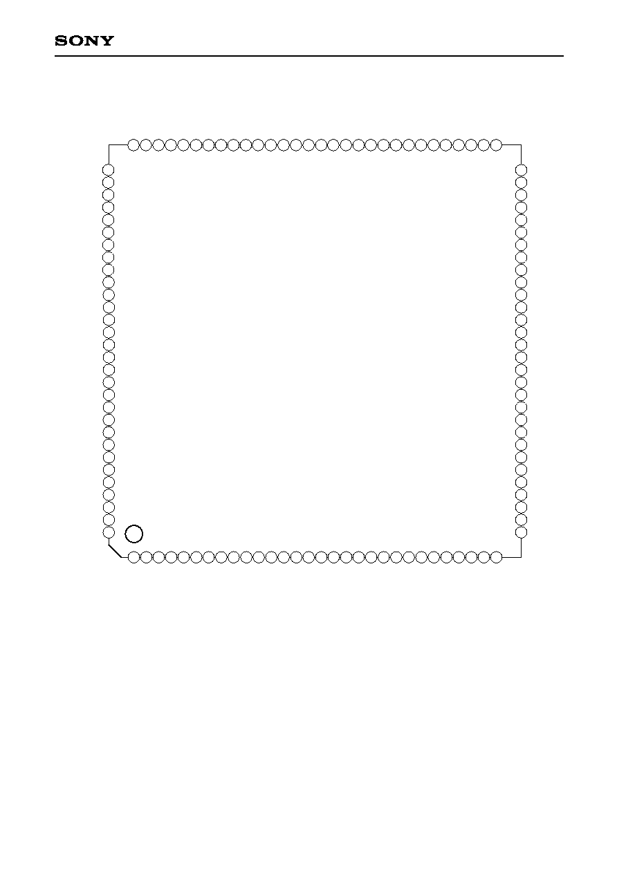
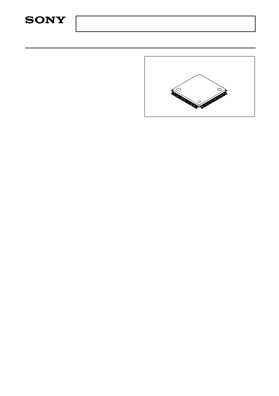
120 pin LQFP (Plastic)
CD Digital Signal Processor with Built-in Digital Servo +
Shock-proof Memory Controller + Digital High & Bass Boost

4
CXD3029R
Pin Description
Pin
No.
1
2
3
4
5
6
7
8
9
10
11
12
13
14
15
16
17
18
19
20
21
22
23
24
25
26
27
28
29
30
31
Power
supply
2-3V
I/F
Digital
O
O
I/O
I/O
I/O
I/O
O
O
O
O
O
O
O
--
O
O
O
I/O
--
I
I
O
I
I
I
O
O
I
I
I/O
I/O
1, 0
1, 0
1, 0
1, 0
1, 0
1, 0
1, 0
1, 0
1, 0
1, 0
1, 0
--
1, 0
1, 0
1, 0
1, 0
--
1, Z, 0
1, 0
1, 0
1, 0
1, 0
DRAM row address strobe signal.
DRAM data input enable signal.
DRAM data bus 1.
DRAM data bus 0.
DRAM data bus 3.
DRAM data bus 2.
Test pin. Do not connect.
Test pin. Do not connect.
DRAM column address strobe signal.
WFCK output. XOE is output by switching with the command.
DRAM address 9.
DRAM address 8.
DRAM address 7.
DRAM interface GND.
DRAM address 6.
DRAM address 5.
DRAM address 4.
DRAM readout enable signal input. XRDE monitor is output by switching
with the command.
Digital power supply.
Serial data transfer clock input from CPU. SQSO and SENS readout
clocks are output by switching with the command.
Serial data input from CPU.
SENS output to CPU. SQSO data is output by switching with the command.
Latch input from CPU. The serial data is latched at the falling edge. XLAT
which is low for 6µs or more is enabled.
CPU serial data output enable signal.
Mute input. Muted when high.
Word clock output f = 2Fs. GRSCOR is output by switching with the command.
High output when the subcode sync is detected. SCOR, which is
interpolated in the IC, is output by switching with the command.
System reset. Reset when low.
Spindle motor external control input.
Subcode Q OK input. XQOK monitor is output by switching with the command.
DRAM write enable signal input. XWRE monitor is output by switching with
the command.
XRAS
XWE
D1
D0
D3
D2
TEST1
TEST2
XCAS
WFCK
A9
A8
A7
DV
SS
A6
A5
A4
XRDE
V
DD
0
CLOK
DATA
SENS
XLAT
XSOE
SYSM
WDCK
SCOR
XRST
PWMI
XQOK
XWRE
Symbol
I/O Value
Description

5
CXD3029R
Pin
No.
32
33
34
35
36
37
38
39
40
41
42
43
44
45
46
47
48
49
50
51
52
53
54
55
56
57
58
59
60
61
62
63
Power
supply
Digital
H/P
X'tal
Lch
Rch
Digital
O
--
I
I
O
O
O
O
I
I
--
O
O
--
I
O
--
O
O
--
--
O
O
--
I
I
--
O
O
I/O
1, 0
--
1, 0
1, 0
1, 0
1, 0
--
1, 0
1, 0
--
--
Analog
Analog
--
--
Analog
Analog
--
--
1, 0
1, 0
1, 0
Microcomputer clock output. R8M and C4M are output by switching with
the command.
Digital GND.
SQSO readout clock input.
SENS serial data readout clock input.
Subcode Q 80-bit and PCM peak and level data output. CD TEXT data output.
DRAM readout prohibited signal.
Write to DRAM prohibited signal.
Subcode P to W serial output.
SBSO readout clock input.
Crystal selection input. Low when the crystal is 16.9344 MHz; high when
the crystal is 33.8688MHz.
Headphone GND.
Lch headphone PDM output.
Rch headphone PDM output.
Headphone power supply.
Master clock power supply.
Crystal oscillation circuit input. The master clock is externally input from
this pin.
Crystal oscillation circuit output.
Master clock GND.
Analog power supply.
Lch analog output.
Lch reference voltage.
Analog GND.
Analog GND.
Rch reference voltage.
Rch analog output.
Analog power supply.
Test pin. Normally GND.
Test pin. Normally GND.
Digital GND.
OR signal output of Lch, Rch "0" detection flag (AND output) and SYSM.
Only "0" detection flag is output by switching with the command.
Digital Out output.
Anti-shock input/output.
R4M
V
SS
0
SQCK
SCLK
SQSO
XEMP
XWIH
SBSO
EXCK
XTSL
HV
SS
HPL
HPR
HV
DD
XV
DD
XTAI
XTAO
XV
SS
AV
DD
1
AOUT1
VREFL
AV
SS
1
AV
SS
2
VREFR
AOUT2
AV
DD
2
TES1
TEST
V
SS
1
LRMU
DOUT
ATSK