 | ÐлекÑÑоннÑй компоненÑ: CXD3519 | СкаÑаÑÑ:  PDF PDF  ZIP ZIP |
Äîêóìåíòàöèÿ è îïèñàíèÿ www.docs.chipfind.ru

1
E00Y07-PS
Sony reserves the right to change products and specifications without prior notice. This information does not convey any license by
any implication or otherwise under any patents or other right. Application circuits shown, if any, are typical examples illustrating the
operation of the devices. Sony cannot assume responsibility for any problems arising out of the use of these circuits.
CXD3519TQ
48 pin TQFP (Plastic)
Reference Voltage and Driver IC for LCD
Description
The CXD3519TQ is suitable IC for applying
reference voltage for gamma correction which is
necessary for TFT liquid crystal display. This IC has
a built-in 9 channels of rail-to-rail buffer circuit which
enables 2-input switch and a common driver circuit.
Features
· Built-in 9 channels of rail-to-rail buffer circuit
· Built-in common driver circuit
· Current consumption: 3.6mA (typ.)
· Package: 48-pin TQFP
Structure
CMOS IC
Applications
Small liquid crystal monitor
Absolute Maximum Ratings (Ta = 25°C)
· Supply voltage
V
DD
V
SS
0.3 to +6.0
V
· Input pin voltage
V
I
V
SS
0.3 to V
DD
+ 0.3 V
· Storage temperature Tstg
55 to +150
°C
· Allowable power dissipation (Ta
85°C)
P
D
220
mW
Operating Conditions
· Supply voltage
V
DD
4.5 to 5.5 (5.0 typ.)
V
· Operating temperature
Topr
35 to +85
°C
2
CXD3519TQ
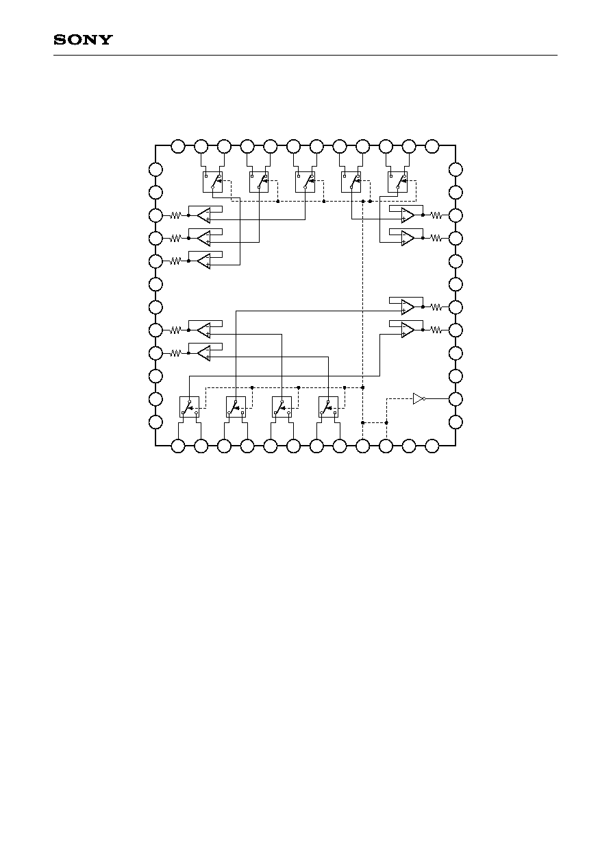
Block Diagram
1
2
3
4
5
6
7
8
9
10
11
12
13
14
15
16
17
18
19
20
21
22
23
24
25
26
27
28
29
30
31
32
33
34
35
36
37
38
39
40
41
42
43
44
45
46
47
48
buff
NC
GND
V6
V5
V4
NC
V
DD
V1
V0
GND
NC
NC
VH3
VL3
VH2
VL2
VH1
VL1
VH0
VL0
SW
SW
GND
NC
NC
VL4
VH4
VL5
VH5
VL6
VH6
VL7
VH7
VL8
VH8
NC
NC
GND
V7
V8
NC
V
DD
V2
V3
GND
V
DD
COMOUT
NC
3
CXD3519TQ
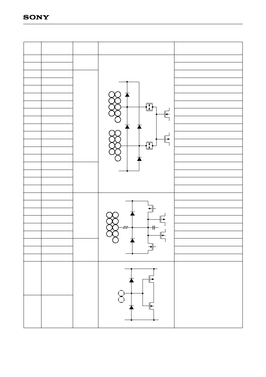
Pin Description
Pin
No.
Symbol
Pin voltage
Equivalent circuit
Description
DC input when SW is high.
DC input when SW is low.
DC input when SW is high.
DC input when SW is low.
DC input when SW is high.
DC input when SW is low.
DC input when SW is high.
DC input when SW is low.
DC input when SW is high.
DC input when SW is low.
DC input when SW is high.
DC input when SW is low.
DC input when SW is high.
DC input when SW is low.
DC input when SW is high.
DC input when SW is low.
DC input when SW is high.
DC input when SW is low.
V0 output.
V1 output.
V2 output.
V6 output.
V7 output.
V8 output.
V3 output.
V4 output.
V5 output.
Input switch.
For V0 to V8 output, VL is
output for low; VH for high.
For COMOUT output, V
DD
level
is output for low; GND level for
high.
Also, Pins 9 and 10 are
connected internally. Input the
same signal, or input one signal
and leave the other signal open.
1
2
3
4
5
6
7
8
26
27
28
29
30
31
32
33
34
35
45
44
18
39
22
21
17
41
40
9
10
VH3
VL3
VH2
VL2
VH1
VL1
VH0
VL0
VH8
VL8
VH7
VL7
VH6
VL6
VH5
VL5
VH4
VL4
V0
V1
V2
V6
V7
V8
V3
V4
V5
SW
SW
0.5 to 4.0V
(max.:
2.0Vp-p)
0.2 to 4.8V
0.5 to 4.0V
(max.:
2.0Vp-p)
0.2 to 4.8V
0.5 to 4.0V
V
DD
VH
VL
GND
1
3
5
7
26
28
30
32
34
2
4
6
8
27
29
31
33
35
V
DD
GND
9
10
V
DD
GND
17
18
21
22
39
40
41
44
45
4
CXD3519TQ
Pin
No.
Symbol
Pin voltage
Equivalent circuit
Description
COM output.
5V power supply.
5V power supply.
5V power supply.
GND.
GND.
GND.
GND.
GND.
No connected.
No connected.
No connected.
No connected.
No connected.
No connected.
No connected.
No connected.
No connected.
No connected.
14
15
19
43
11
16
23
38
46
12
13
20
24
25
36
37
42
47
48
COMOUT
V
DD
V
DD
V
DD
GND
GND
GND
GND
GND
NC
NC
NC
NC
NC
NC
NC
NC
NC
NC
5.0V
5.0V
5.0V
Note)
· GND
Make sure that Pins 11, 16, 23, 38 and 46 are connected to GND potential, and do not release them.
· Decoupling capacitor
Locate decoupling capacitor connected between power supply and GND as near IC pin as possible.
· Design VH and VL input pins not to have capacity.
V
DD
GND
COMOUT 14
5
CXD3519TQ
Electrical Characteristics
(Ta = 25°C, V
DD
= 5V)
No.
1
2
3
4
5
6
7
8
9
10
11
12
13
14
15
16
17
18
Item
Current consumption
VH, VL input current high
VH, VL input current low
SW input current high
SW input current low
VREF voltage gain
SW input voltage high
SW input voltage low
VREF output voltage high
VREF output voltage low
COMOUT output voltage high
COMOUT output voltage low
VREF offset voltage
VREF (V0, 1, 2, 6, 7, 8)
load regulation 1
VREF (V3, 4, 5)
load regulation 2
Setting time 1
Setting time 2
Output impedance
Symbol
I
CC
I
IH
I
IL
I
ISH
I
ISL
AV
V
IH
V
IL
V
OH
V
OL
V
COH
V
COL
V
OFF
V
O
1
V
O
2
ts1
ts2
ts3
ts4
Rimp
Conditions
Input voltage = 2.5V, No load
Input voltage = 4.8V
Input voltage = 0.2V
Input voltage = 5V
Input voltage = 0V
Input voltage = 0.2 to 4.8V
I
SOURCE
= 10mA
I
SINK
= 10mA
I
SOURCE
= 10mA
I
SINK
= 10mA
Input voltage = 0.2 to 4.8V
I
SOURCE
= 10mA
I
SINK
= 10mA
Input voltage = 0.5 to 4.0V
I
SOURCE
= 10mA
I
SINK
= 10mA
Measurement circuits 1, 2
Measurement circuit 3
V0 V8
Min.
--
0.1
0.1
10
10
0.985
2.0
--
V
DD
1.0
--
V
DD
0.1
--
--
--
--
--
--
--
Typ.
3.6
--
--
--
--
--
--
--
--
--
--
--
--
±5
±7
--
--
15
Max.
6.0
0.1
0.1
10
10
--
--
0.8
--
GND + 1.0
--
GND + 0.1
20
±10
±14
10
6
--
Unit
mA
µA
µA
µA
µA
V/V
V
V
V
V
V
V
mV
mV
mV
µs
µs