 | –≠–ª–µ–∫—Ç—Ä–æ–Ω–Ω—ã–π –∫–æ–º–ø–æ–Ω–µ–Ω—Ç: CXD3609R | –°–∫–∞—á–∞—Ç—å:  PDF PDF  ZIP ZIP |

≠ 1 ≠
E02634-PS
Sony reserves the right to change products and specifications without prior notice. This information does not convey any license by
any implication or otherwise under any patents or other right. Application circuits shown, if any, are typical examples illustrating the
operation of the devices. Sony cannot assume responsibility for any problems arising out of the use of these circuits.
CXD3609R
48 pin LQFP (Plastic)
Timing Generator for Progressive Scan CCD Image Sensor
Description
The CXD3609R is a timing generator IC which
generates the timing pulses for performing progressive
scan using the ICX274 CCD image sensor.
Features
∑ Base oscillation frequency 57.2/72MHz
∑ Electronic shutter function
∑ Supports draft/monitoring mode
∑ Trigger shutter function
∑ Vertical driver for CCD image sensor
Applications
∑ Digital still cameras
∑ Image processor
Structure
Silicon gate CMOS IC
Applicable CCD Image Sensors
ICX274 (Type 1/1.8, 2020K pixels)
Pin Configuration
Absolute Maximum Ratings
∑ Supply voltage
V
DD
Vss ≠ 0.3 to +7.0
V
VL
≠10.0 to Vss
V
VH
VL ≠ 0.3 to +26.0
V
∑ Input voltage
V
I
Vss ≠ 0.3 to V
DD
+ 0.3
V
∑ Output voltage
V
O1
Vss ≠ 0.3 to V
DD
+ 0.3
V
V
O2
VL ≠ 0.3 to V
SS
+ 0.3
V
V
O3
VL ≠ 0.3 to VH + 0.3
V
∑ Operating temperature
Topr
≠20 to +75
∞C
∑ Storage temperature
Tstg
≠55 to +150
∞C
Recommended Operating Conditions
∑ Supply voltage
V
DD
a
3.0 to 5.25
V
V
DD
b, V
DD
c 3.0 to 3.6
V
VM
0.0
V
VH
14.5 to 15.5
V
VL
≠7.0 to ≠8.0
V
∑ Operating temperature
Topr
≠20 to +75
∞C
Groups of pins enclosed in the figure indicate
sections for which power supply separation is
possible.
1
2
3
4
5
6
7
8
9
10
11
12
13
14
15
16
17
18
19
20
21
22
23
24
25
26
27
28
29
30
31
32
33
34
35
36
37
38
39
40
41
42
43
44
45
46
47
48
H2A
V
SS
3
H2B
V
DD
3
V
DD
4
XSHP
XSHD
PBLK
CLPDM
OBCLP
ADCLK
V
SS
4
CK
O
CKI
TEST
TRIG
V
DD
5
MCK
O
SSI
SCK
SEN
VR
HR
V
SS
5
H1B
V
DD
2
H1A
V
SS
2
RG
SSGSL
V
DD
1
WEN
ID/EXP
SNCSL
RST
V
SS
1
SUB
V3C
V3B
VL
V3A
V2C
V2B
VH
V2A
V4
V1
VM
≠ 2 ≠
CXD3609R
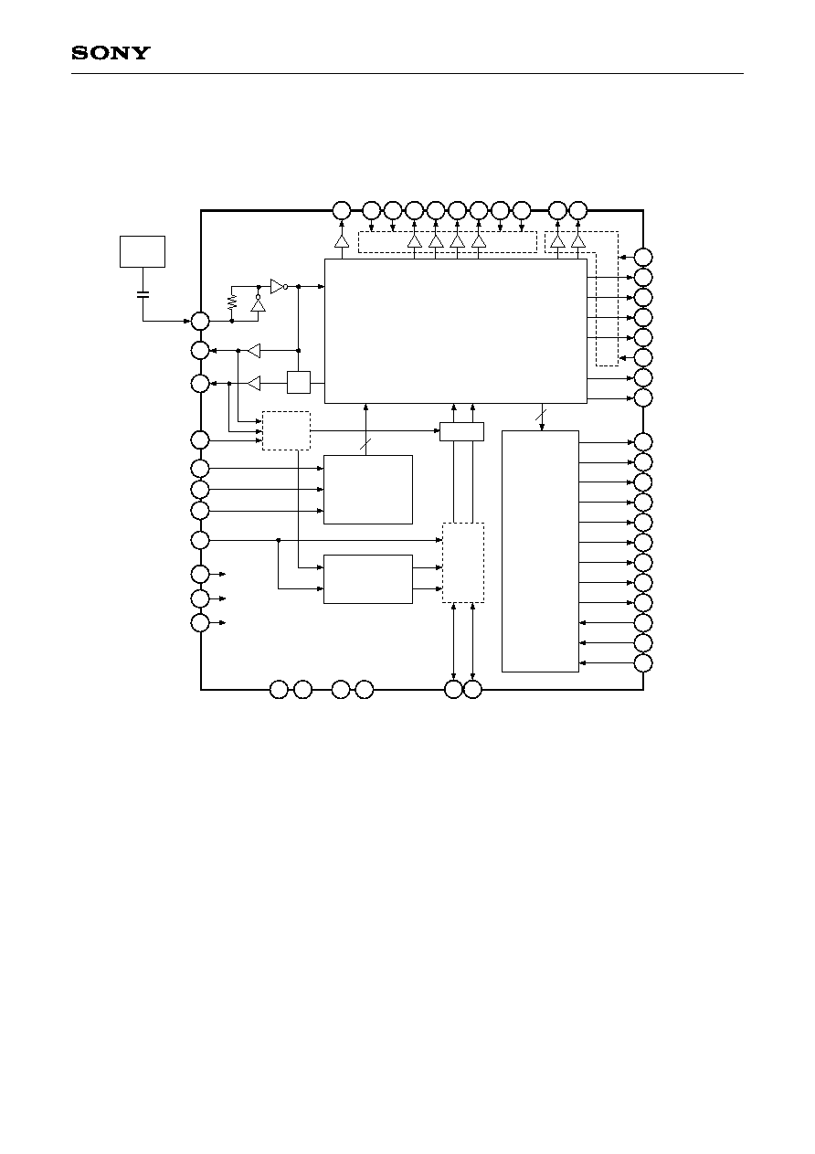
Block Diagram
35 34
42
43
40
38
5
4
22
21
20
26
30
25
V2A
V2B
V2C
V1
WEN
ID/EXP
OBCLP
CLPDM
PBLK
24
17
V
SS
4
V
DD
4
VR
HR
36
7
V
DD
1
1
29
V
DD
5
V
SS
1
V
SS
5
MCKO
CKO
CKI
2
27
TEST
RST
28
TRIG
23 ADCLK
41
48
39
47
46
44
VM
SUB
V4
V3C
V3B
V3A
45
37
VL
VH
31
32
33
SEN
SCK
SSI
V Driver
3
SNCSL
1/2
19
18
XSHD
XSHP
9
13
10
16
V
SS
2
H2A
H1A
V
DD
3
12
H1B
8
RG
15
H2B
11
V
DD
2
14
V
SS
3
Selector
Selector
Latch
Register
Pulse Generator
CKI
SSG
6
SSGSL

≠ 3 ≠
CXD3609R
Pin Description
Pin
No.
1
2
3
4
5
6
7
8
9
10
11
12
13
14
15
16
17
18
19
20
21
22
23
24
25
26
Symbol
I/O
--
I
I
O
O
I
--
O
--
O
--
O
O
--
O
--
--
O
O
O
O
O
O
--
O
I
Description
GND
Internal system reset input. High: Normal operation, Low: Reset control.
Normally apply reset during power-on.
Schmitt trigger input/protective diode on power supply side
Control input used to switch sync system. High: CKI sync, Low: MCKO sync.
With pull-down resistor
Vertical direction line identification pulse output/exposure time identification
pulse output.
Switching possible using the serial interface data. (Default: ID)
Memory write timing pulse output.
Internal SSG enable. High: Internal SSG valid, Low: External sync valid.
With pull-down resistor
3.3V power supply. (Power supply for common logic block)
CCD reset gate pulse output.
Logic phase adjustment possible using the serial interface data.
GND
CCD horizontal register clock output.
Logic phase adjustment possible using the serial interface data.
5/3.3V power supply. (Power supply for H)
CCD horizontal register clock output.
Logic phase adjustment possible using the serial interface data.
CCD horizontal register clock output.
Logic phase adjustment possible using the serial interface data.
GND
CCD horizontal register clock output.
Logic phase adjustment possible using the serial interface data.
5/3.3V power supply. (Power supply for H)
3.3V power supply. (Power supply for CDS)
CCD precharge level sample-and-hold pulse output.
Logic phase adjustment possible using the serial interface data.
CCD data level sample-and-hold pulse output.
Logic phase adjustment possible using the serial interface data.
Pulse output for horizontal and vertical blanking period pulse cleaning.
CCD dummy signal clamp pulse output.
CCD optical black signal clamp pulse output.
The horizontal OB pattern can be changed using the serial interface data.
Clock output for analog/digital conversion IC.
Logic phase adjustment possible using the serial interface data.
GND
Inverter output.
Inverter input.
V
SS
1
RST
SNCSL
ID/EXP
WEN
SSGSL
V
DD
1
RG
V
SS
2
H1A
V
DD
2
H1B
H2A
V
SS
3
H2B
V
DD
3
V
DD
4
XSHP
XSHD
PBLK
CLPDM
OBCLP
ADCLK
V
SS
4
CKO
CKI

≠ 4 ≠
CXD3609R
Pin
No.
27
28
29
30
31
32
33
34
35
36
37
38
39
40
41
42
43
44
45
46
47
48
Symbol
TEST
TRIG
V
DD
5
MCKO
SSI
SCK
SEN
VR
HR
V
SS
5
VM
V1
V4
V2A
VH
V2B
V2C
V3A
VL
V3B
V3C
SUB
I/O
I
I
--
O
I
I
I
I/O
I/O
--
I
O
O
O
--
O
O
O
--
O
O
O
Description
IC test pin. normally fixed to GND.
With pull-down resistor
Trigger mode. Normally fix to power supply.
3.3V power supply. (Power supply for common logic block)
System clock output for signal processing IC.
Serial interface data input for internal mode settings.
Schmitt trigger input/protective diode on power supply side.
Serial interface data input for internal mode settings.
Schmitt trigger input/protective diode on power supply side.
Serial interface data input for internal mode settings.
Schmitt trigger input/protective diode on power supply side.
Vertical sync signal input/output.
Horizontal sync signal input/output.
GND
GND (GND for vertical driver)
CCD vertical register clock output.
CCD vertical register clock output.
CCD vertical register clock output.
15.0V power supply. (Power supply for vertical driver)
CCD vertical register clock output.
CCD vertical register clock output.
CCD vertical register clock output.
≠7.5V power supply. (Power supply for vertical driver)
CCD vertical register clock output.
CCD vertical register clock output.
CCD electronic shutter pulse output.
≠ 5 ≠
CXD3609R
Electrical Characteristics
DC Characteristics
(Within the recommended operating conditions)
1
These input pins are Schmitt trigger inputs, and have a protective diode on the power supply side in the IC.
Therefore, they do not support 5V input.
2
This input pin is with pull-down resistor in the IC.
Note) The above table indicates the condition for 3.3V drive.
Item
Pins
Symbol
Conditions
Min.
Typ.
Max.
Unit
Supply
voltage 1
Supply
voltage 2
Supply
voltage 3
Input
voltage 1
1
Input
voltage 2
2
Input
voltage 3
Input/output
voltage
Output
voltage 1
Output
voltage 2
Output
voltage 3
Output
voltage 4
Output
voltage 5
Output
current 1
Output
current 2
V
DD
2, V
DD
3
V
DD
4
V
DD
1, V
DD
5
RST, SSI,
SCK, SEN
SNCSL,
SSGSL, TEST
TRIG
VR, HR
H1A, H1B,
H2A, H2B
XSHP, XSHD,
PBLK, ADCLK,
OBCLP,
CLPDM
CKO
RG, MCKO
ID/EXP,
WEN
V2A/B/C,
V3A/B/C,
V1, V4
SUB
V
DD
a
V
DD
b
V
DD
c
Vt
+
Vt
≠
V
IH1
V
IL1
V
IH1
V
IL1
V
IH2
V
IL2
V
OH1
V
OL1
V
OH2
V
OL2
V
OH3
V
OL3
V
OH4
V
OL4
V
OH5
V
OL5
V
OH6
V
OL6
I
OL
I
OM1
I
OM2
I
OH
I
OSL
I
OSH
Feed current where I
OH
= ≠1.2mA
Pull-in current where I
OL
= 2.4mA
Feed current where I
OH
= ≠22.0mA
Pull-in current where I
OL
= 14.4mA
Feed current where I
OH
= ≠3.3mA
Pull-in current where I
OL
= 2.4mA
Feed current where I
OH
= ≠6.9mA
Pull-in current where I
OL
= 4.8mA
Feed current where I
OH
= ≠3.3mA
Pull-in current where I
OL
= 2.4mA
Feed current where I
OH
= ≠2.4mA
Pull-in current where I
OL
= 4.8mA
V1, V2A to C, V3A to C, V4 = ≠8.25V
V1, V2A to C, V3A to C, V4 = ≠0.25V
V2A to C, V3A to C = 0.25V
V2A to C, V3A to C = 14.75V
SUB = ≠8.25V
SUB = 14.75V
3.0
3.0
3.0
0.8V
DD
c
0.7V
DD
c
0.8V
DD
c
0.8V
DD
c
V
DD
c ≠ 0.8
V
DD
a ≠ 0.8
V
DD
b ≠ 0.8
V
DD
c ≠ 0.8
V
DD
c ≠ 0.8
V
DD
c ≠ 0.8
10.0
5.0
5.4
3.3
3.3
3.3
5.25
3.6
3.6
0.2V
DD
c
0.3V
DD
c
0.2V
DD
c
0.2V
DD
c
0.4
0.4
0.4
0.4
0.4
0.4
≠5.0
≠7.2
≠4.0
V
V
V
V
V
V
V
V
V
V
V
V
V
V
V
V
V
V
V
V
V
V
V
mA
mA
mA
mA
mA
mA

≠ 6 ≠
CXD3609R
Inverter Input Characteristics for Base Oscillation Clock Duty Adjustment
Item
Logical Vth
Input voltage
Input amplitude
Pins
CKI
Symbol
LVth
V
IH
V
IL
V
IN
Conditions
fmax = 50MHz sine wave
Min.
0.7V
DD
c
0.3
Typ.
V
DD
c/2
Max.
0.3V
DD
c
Unit
V
V
V
Vp-p
Note) Input voltage is the input voltage characteristics for direct input from an external source.
Input amplitude is the input amplitude characteristics in the case of input through a capacitor.
Switching Characteristics
(VH = 15.0V, VM = GND, VL = ≠7.5V)
Item
Rise time
Fall time
Output noise voltage
Symbol
TTLM
TTMH
TTLH
TTML
TTHM
TTHL
VCLH
VCLL
VCMH
VCML
Conditions
VL to VM
VM to VH
VL to VH
VM to VL
VH to VM
VH to VL
Min.
200
200
30
200
200
30
Typ.
350
350
60
350
350
60
Max.
500
500
90
500
500
90
1.0
1.0
1.0
1.0
Unit
ns
ns
ns
ns
ns
ns
V
V
V
V
Notes)
1) The MOS structure of this IC has a low tolerance for static electricity, so full care should be given for
measures to prevent electrostatic discharge.
2) For noise and latch-up countermeasures, be sure to connect a by-pass capacitor (0.1µF or more)
between each power supply pin (VH, VL) and GND.
3) To protect the CCD image sensor, clamp the SUB pin output at VH before input to the CCD image sensor.

≠ 7 ≠
CXD3609R
Switching Waveforms
Waveform Noise
V2A (V2B, V2C, V3A, V3B, V3C)
V1 (V4)
SUB
TTMH
TTHM
VH
VM
VL
VM
VL
VH
VL
90%
10%
90%
10%
TTLM
TTLM
90%
10%
90%
10%
TTLH
TTHL
90%
90%
10%
10%
TTML
90%
10%
TTML
90%
10%
VCMH
VCML
VM
VL
VCLH
VCLL
≠ 8 ≠
CXD3609R
Measurement Circuit
1
2
3
4
5
6
7
8
9
11 12
13
14
15
16
17
18
19
20
21
22
23
24
25
27
28
29
30
31
32
33
34
35
36
37
38
39
40
41
42
43
44
45
46
47
48
VR
CKI
C6
C6
C6
C6
C6
C6
C6
C6
C5
C5
C5
C5
C4
C3
CXD3609R
Serial interface data
HR
+3.3V
≠7.5V
+15.0V
C2
C2
C2
C2
C2
R1
R1
R1
R2
R1
R1
R1
C2
C2
C2
C2
C2
C2
C2
C2
C2
C1
C1
C1
C1
C1
C1
C2
26
10
C1: 3300pF
C2: 560pF
C3: 820pF
C4: 2pF
C5: 97pF at 4-ch output
C6: 10pF
R1: 30
R2: 10
194pF at 2-ch output

≠ 9 ≠
CXD3609R
AC Characteristics
AC characteristics between the serial interface clocks
(Within the recommended operating conditions)
Symbol
t
s1
t
h1
t
s2
t
s3
Definition
SSI setup time, activated by the rising edge of SCK
SSI hold time, activated by the rising edge of SCK
SCK setup time, activated by the rising edge of SEN
SEN setup time, activated by the rising edge of SCK
Min.
20
20
20
20
Typ.
Max.
Unit
ns
ns
ns
ns
Serial interface clock internal loading characteristics (1)
Be sure to maintain a constantly high SEN logic level near the falling edge of the HR in the horizontal
period during which V2A/B/C and V3A/B/C values take the ternary value and during that horizontal period.
(Within the recommended operating conditions)
Symbol
t
s1
t
h1
Definition
SEN setup time, activated by the falling edge of HR
SEN hold time, activated by the falling edge of HR
Min.
0
53
Typ.
Max.
Unit
ns
µs
SSI
0.2V
DD
c
0.2V
DD
c
0.8V
DD
c
ts2
th1
ts1
ts3
0.8V
DD
c
0.8V
DD
c
SCK
SEN
SEN
VR
HR
HR
SEN
th1
ts1
Enlarged view
Example: During progressive scan (high-speed sweep present)
V2A
V2A
0.2V
DD
c
0.8V
DD
c
0.2V
DD
c
Restriction for the operating frequency of 36MHz.

≠ 10 ≠
CXD3609R
Serial interface clock internal loading characteristics (2)
Be sure to maintain a constantly high SEN logic level near the falling edge of VR.
(Within the recommended operating conditions)
Symbol
t
s1
t
h1
Definition
SEN setup time, activated by the falling edge of VR
SEN hold time, activated by the falling edge of VR
Min.
0
200
Typ.
Max.
Unit
ns
ns
Serial interface clock output variation characteristics
Normally, the serial interface data is loaded to the CXD3609R at the timing shown in "Serial interface clock
internal loading characteristics (1)" above. However, one exception to this is when the data such as STB is
loaded to the CXD3609R and controlled at the rising edge of SEN. See "Description of Operation".
(Within the recommended operating conditions)
Symbol
t
pdPULSE
Definition
Output signal delay, activated by the rising edge of SEN
Min.
10
Typ.
Max.
100
Unit
ns
VR
HR
SEN
th1
ts1
VR
HR
0.2V
DD
c
0.8V
DD
c
0.2V
DD
c
Enlarged view
Example: During progressive scan (high-speed sweep present)
RST loading characteristics
(Within the recommended operating conditions)
Symbol
t
w1
Definition
RST pulse width
Min.
35
Typ.
Max.
Unit
ns
RST
0.2V
DD
c
tw1
0.8V
DD
c
0.8V
DD
c
SEN
Output signal
tpdPULSE

≠ 11 ≠
CXD3609R
VR and HR phase characteristics
(Within the recommended operating conditions)
Symbol
t
s1
t
h1
Definition
VR setup time, activated by the falling edge of HR
VR hold time, activated by the falling edge of HR
Min.
0
0
Typ.
Max.
Unit
ns
ns
HR loading characteristics
MCKO load capacitance = 10pF
(Within the recommended operating conditions)
Symbol
t
s1
t
h1
Definition
HR setup time, activated by the rising edge of MCKO
HR hold time, activated by the rising edge of MCKO
Min.
13
0
Typ.
Max.
Unit
ns
ns
Output variation characteristics
WEN and ID/EXP load capacitance = 10pF
(Within the recommended operating conditions)
Symbol
t
pd1
Definition
Time until the above outputs change after the rise of MCKO
Min.
20
Typ.
Max.
60
Unit
ns
0.2V
DD
c
VR
HR
ts1
th1
0.2V
DD
c
0.2V
DD
c
0.8V
DD
c
HR
MCKO
ts1
th1
0.2V
DD
c
0.2V
DD
c
0.8V
DD
c
MCKO
WEN, ID/EXP
tpd1

≠ 12 ≠
CXD3609R
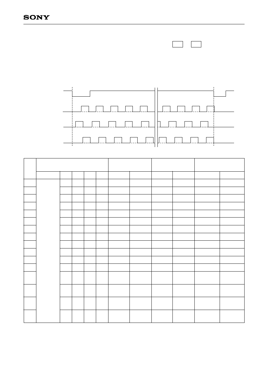
Description of Operation
Pulses output from the CXD3609R are controlled mainly by the RST pin and by the serial interface data. The
Pin Status Table is shown below, and the details of serial interface control are described on the following
pages.
Pin Status Table
1
It is for output. For input, all items are "ACT".
Note) ACT means that the circuit is operating, and DIS means that loading is stopped. L indicates a low
output level, and H a high output level in the controlled status.
Also, VH, VM and VL indicate the voltage levels applied to VH (Pin 41), VM (Pin 37) and VL (Pin 45),
respectively, in the controlled status. Note that in sleep mode and standby mode, VH and VL power
supply should be stopped together with the CCD image sensor.
L
ACT
--
ACT
--
L
ACT
ACT
ACT
L
L
--
--
VM
VM
VM
--
VM
VM
VM
--
VM
VM
VH
Pin
No.
1
2
3
4
5
6
7
8
9
10
11
12
13
14
15
16
17
18
19
20
21
22
23
24
Symbol
V
SS
1
RST
SNCSL
ID/EXP
WEN
SSGSL
V
DD
1
RG
V
SS
2
H1A
V
DD
2
H1B
H2A
V
SS
3
H2B
V
DD
3
V
DD
4
XSHP
XSHD
PBLK
CLPDM
OBCLP
ADCLK
V
SS
4
CAM
SLP
STB
RST
Pin
No.
25
26
27
28
29
30
31
32
33
34
35
36
37
38
39
40
41
42
43
44
45
46
47
48
Symbol
CKO
CKI
TEST
TRIG
V
DD
5
MCKO
SSI
SCK
SEN
VR
HR
V
SS
5
VM
V1
V4
V2A
VH
V2B
V2C
V3A
VL
V3B
V3C
SUB
CAM
SLP
STB
RST
ACT
ACT
ACT
ACT
ACT
ACT
ACT
ACT
ACT
ACT
ACT
ACT
ACT
ACT
ACT
ACT
ACT
ACT
ACT
ACT
ACT
ACT
ACT
ACT
ACT
L
L
VM
VM
VH
VH
VH
VH
VH
VH
VH
L
ACT
ACT
L
ACT
ACT
ACT
L
L
VM
VM
VH
VH
VH
VH
VH
VH
VH
ACT
ACT
DIS
ACT
DIS
DIS
DIS
H
H
VM
VL
VM
VM
VM
VL
VL
VL
VL
SST
SST
--
ACT
ACT
L
L
ACT
--
L
--
L
--
L
L
--
L
--
--
L
L
L
L
L
L
--
ACT
ACT
ACT
ACT
ACT
ACT
ACT
ACT
ACT
ACT
ACT
ACT
ACT
ACT
ACT
ACT
ACT
ACT
L
L
ACT
L
L
L
L
L
L
L
L
L
L
L
ACT
ACT
L
L
ACT
L
L
L
L
L
L
L
L
L
L
L
L
ACT
L
L
ACT
ACT
ACT
ACT
ACT
ACT
ACT
ACT
H
H
H
ACT

≠ 13 ≠
CXD3609R
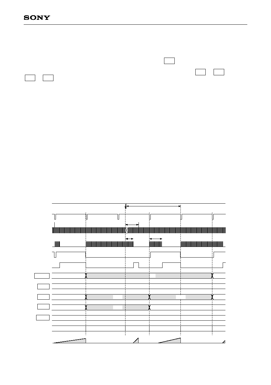
Serial Interface Control
The CXD3609R basically loads and reflects the serial interface data sent in the following format. The position
at which the data is reflected differs depending on the data, but normally the data is reflected at the rising edge
of SEN, the falling edge of VR, or immediately before the readout block. See the load column for the reflection
position of each data.
Note that as an exception, data loading is subject to restrictions during trigger shutter drive and long-time
exposure. See these separate items for details.
There are three categories of serial interface data: the CXD3609R drive control data (hereafter "control data"),
electronic shutter data (hereafter "shutter data") and trigger shutter data (hereafter "TRIG data").
The details of each data are described below.
SSI
SCK
SEN
00
01
02
03
04
05
06
07
42
43
41
44
45
46
47

≠ 14 ≠
CXD3609R
Data
D00
to
D07
D08,
D09
D10,
D11
D12
to
D15
D16
D17
D18,
D19
D20
to
D22
D23
D24,
D25
D26,
D27
D28,
D29
D30,
D31
D32
D33
D34,
D35
D36,
D37
D38,
D39
D40
to
D47
Symbol
CHIP
CTG
--
MODE
OSCH
TRIGSL
SMD
--
STPHS
LDHS
LDRG
LDSP
LDSD
--
EXP
PTOB
LDAD
STB
--
Function
Chip enbale
Category switching
--
Drive mode switching
Base oscillation switching
TRIG control switching
Electronic shutter mode switching
--
H block stop control (2ch)
H block logic phase adjustment
RG logic phase adjustment
XSHP logic phase adjustment
XSHD logic phase adjustment
--
ID/EXP output switching
OBCLP waveform pattern switching
ADCLK logic phase adjustment
Standby control
--
Data = 1
10000001
Enabled
Other values
Disabled
See Category.
--
--
See Drive mode.
28MHz
36MHz
OFF
ON
See Electronic shutter mode switching.
--
--
4ch
2ch
See Logic phase adjustment.
See Logic phase adjustment.
See Logic phase adjustment.
See Logic phase adjustment.
--
--
ID
EXP
See OBCLP waveform pattern.
See Logic phase adjustment.
See Standby.
--
--
Control Data
RST
All
0
All
0
All
0
All
0
0
0
All
0
All
0
0
All
0
All
0
All
0
All
0
0
0
All
0
1
0
All
0
All
0
Data = 0

≠ 15 ≠
CXD3609R
Data
D00
to
D07
D08,
D09
D10
to
D13
D14
to
D23
D24
to
D35
D36,
D37
D38
to
D47
Symbol
CHIP
CTG
--
SVR
SHR
--
SPL
Function
Chip enable
Category switching
--
Electronic shutter vertical period
specification
Electronic shutter horizontal period
specification
--
High-speed shutter position
specification
Data = 0
Data = 1
10000001
Enabled
Other values
Disabled
See Category.
--
--
See Electronic shutter.
See Electronic shutter.
--
--
See Electronic shutter.
Shutter Data
RST
All
0
All
0
All
0
All
0
All
0
All
0
All
0
≠ 16 ≠
CXD3609R
Data
D00
to
D07
D08,
D09
D10,
D11
D12
D13
to
D23
D24
to
D35
D36
to
D40
D42
to
D47
Symbol
CHIP
CTG
--
TRHS
TRSH
TRSG
--
SINT
Function
Chip enable
Category switching
--
(Under trigger shutter drive)
High-speed sweep switching
(Under trigger shutter drive)
Electronic shutter horizontal period
specification
(Under trigger shutter drive)
SG generation position specification
--
Electronic shutter fine adjustment
specification
Data = 0
Data = 1
10000001
Enabled
Other values
Disabled
See Category.
--
--
Present
Not present
See Trigger shutter.
See Trigger shutter.
--
--
See Electronic shutter.
TRIG Data
RST
All
0
All
0
All
0
All
0
All
0
All
0
All
0
All
0

≠ 17 ≠
CXD3609R
Detailed Description of Each Data
Shared data: D08 and D09 CTG [Category]
Of the data provided to the CXD3609R by the serial interface, the CXD3609R loads D10 and subsequent
data to each data register as shown in the table below according to the combination of D08 and D09 .
D09
0
0
1
1
D08
0
1
0
1
Description of operation
Loading to control data register
Loading to shutter data register
Loading to TRIG data register
Test mode
Note that the CXD3609R can apply these categories consecutively within the same vertical period. However,
care should be taken as the data is overwritten if the same category is applied.

≠ 18 ≠
CXD3609R
Control data: D12 to D15 MODE [Drive mode]
The CXD3609R realizes various drive modes using control data D12 to D15 MODE.
The drive mode-related bits are loaded to the CXD3609R and reflected at the falling edge of VR.
The details are described below.
The various basic drive modes are switched using the upper two bits D12 and D13 of the control data
MODE.
Draft mode is the mode called 2/4-line readout mode in the ICX274.
Monitoring mode is the mode called 2/8-line readout mode in the ICX274. This is a drive mode with an even
higher frame rate than draft mode that can be used for purposes such as monitoring and auto focus (AF).
Progressive scan mode is the ICX274 drive mode in which the data for all lines are read. Vertical transfer high-
speed sweep period present/not present can be selected.
See the ICX274 data sheet for details of the readout lines for other modes.
The periods and Timing Charts when each mode is driven with the internal SSG are listed below.
D14
0
1
0
1
Description of operation
(D13/12) = (0, 0)
Draft
Draft
Center scan 1
Center scan 2
D15
0
0
1
1
(D13/12) = (0, 1)
Monitoring
Monitoring
AF1
AF2
(D13/12) = (1, 0)
Progressive scan (high-
speed sweep not present)
Progressive scan (high-
speed sweep not present)
Center scan 3
Progressive scan (high-
speed sweep present)
(D13/12) = (1, 1)
Addition 1
Addition 1
Addition 1
Addition 1
Progressive scan
Progressive scan
≠ High-speed sweep ≠
Center scan 3
Draft
Addtion
Center scan 1
Center scan 2
Monitoring
AF1
AF2
Mode
Drive
frequency
fps
Internal SSG period
Hotizontal
Vertical
Normal
High-speed sweep
Frame shift
Readout
1920ck
2070ck
2352ck
Chart-11
Chart-13
Chart-12
1492H + 1860ck
1251H + 480ck
1741H + 1530ck
1563H + 1021ck
◊
2
497H + 1260ck
625H + 1200ck
692H + 810ck
870H + 900ck
692H + 810ck
870H + 900ck
461H + 1230ck
580H + 601ck
461H + 1230ck
580H + 601ck
405H + 1470ck
◊
2
510H + 1680ck
202H + 1323ck
◊
2
255H + 840ck
101H + 1323ck
127H + 1596ck
Chart-1
Chart-4
Chart-7
Chart-7.1
Chart-2
Chart-10
Chart-5
Chart-5.1
Chart-6
Chart-6.1
Chart-3
Chart-8
Chart-8.1
Chart-9
Chart-9.1
Chart-23
Chart-29
Chart-25
Chart-26
Chart-27
Chart-28
Chart-24
Chart-30
--
Chart-4
Chart-16
--
Chart-15
--
Chart-17
Chart-18
--
Chart-20
--
Chart-19
--
Chart-21
Chart-22
28
36
28
36
28
36
28
36
28
36
28
36
28
36
28
36
28
36
28
36
10
15
30
20
30
60
120
V-Chart
H-Chart
≠ 19 ≠
CXD3609R
Control data: D16 OSCH [Drive frequency pattern switching]
This switches the internal SSG VR pattern. Change the base oscillation frequency applied to CKI to match
each pattern.
D14
0
1
Description of operation
28MHz operation drive
36MHz operation drive
Control data: D17 TRIGSL [TRIG control switching]
This sets the TRIG pulse standby mode for performing TRIG drive. See TRIG control for a detailed description
of TRIG drive.
Control data: D18 and D19 SMD [Electronic shutter mode switching]
This enables the various electronic shutter settings. See Shutter control for a detailed description of shutter
drive.
D19
0
0
1
1
Description of operation
Electronic shutter off
Electronic shutter on
Readout stopped setting, electronic shutter off
Readout stopped setting, a part of electronic shutter enabled
D18
0
1
0
1
Control data: D23 STPHS [H block stop control]
This adjusts the driving capability by outputting the H driver output on 4ch or 2ch.
During 2ch output, the H1B and H2B pins are stopped. In addition, the load applied to the CXD3609R
increases during 2ch output, so use of an external driver should also be considered depending on the
situation.
D23
0
1
Description of operation
4ch output
2ch output
Control data: D24 and D25 LDHS [H block logic phase]
This indicates the H block logic phase adjustment data. The default is 0∞.
D25
0
0
1
1
D24
0
1
0
1
Degree of adjustment (∞)
0
90
180
270
Control data: D26 to D31 LDRG, LDSP, LDSD [Each pulse logic phase]
These indicate the RG, XSHP and XSHD logic phase adjustment data. The adjustment width is the same as
for LDHS. The default is 0∞.
≠ 20 ≠
CXD3609R
Control data: D33 EXP [ID/EXP output switching]
The ID/EXP pin (Pin 4) output can be switched to the ID pulse or the EXP pulse using D33 EXP. The default
is the "ID" pulse. See the Timing Charts for the ID pulse.
The EXP pulse indicates the exposure time when it is high. Normally, high is indicated from the falling edge of
the last SUB to the falling edge of the next SG.
Note that the EXP pulse changes as follows when SUB does not rise.
Mode
Draft, 2-line addition 2, center scan 1
2-line addition 1, center scan 2
Monitoring, progressive scan, center scan 3, AF1, AF2
Last SG generation position
600, 750ck
1128, 1278ck
1100, 1250ck
EXP pulse rise point
804ck
1296ck
1322ck
Also, switching between ID and EXP is performed at the ID reset timing (the ID transition point during the
horizontal period with each V1A/B/C and V3A/B/C ternary output), and the pulse is also reset to low at this point.
See the explanatory diagrams under Electronic shutter for an image of ID/EXP pulse changes.
Control data: D34 and D35 PTOB [OBCLP waveform pattern]
This indicates the OBCLP waveform pattern. The default is "Normal".
Control data: D36 and D37 LDAD [ADCLK logic phase]
This indicates the ADCLK logic phase adjustment data. The default is "90∞" relative to MCKO.
D37
0
0
1
1
D36
0
1
0
1
Degree of adjustment (∞)
0
90
180
270
Control data: D38 and D39 STB [Standby]
The operating mode is switched as follows. However, the standby bits are loaded to the CXD3609R and control
is applied immediately at the rising edge of SEN.
See the Pin Status Table for the pin status in each mode.
D39
X
0
1
1
D38
0
1
0
1
Operating mode
CAM
SLP
SST
STB
Normal operating mode
Sleep mode
Siesta mode
Standby mode
Symbol
D35
0
0
1
1
D34
0
1
0
1
Waveform pattern
(Normal)
(Shifted rearward)
(Shifted forward)
(Wide)

≠ 21 ≠
CXD3609R
Shutter data: [Electronic shutter]
The CXD3609R realizes various electronic shutter functions by using shutter data D18 and D19 SMD and
shutter data D14 to D23 SVR, D24 to D35 SHR, D38 to D47 SPL and TRIG data D42 to D47 SINT.
These functions are described in detail below.
First, the various modes are shown below. These modes are switched using control data D13 and D14 SMD.
MSB
D35
X
D34
0
D33
0
D32
1
D31
1
D30
1
D29
0
D28
0
LSB
1
C
SHR is expressed
as 1C3h .
D27
0
D26
0
D25
1
D24
1
3
[Electronic shutter stopped mode]
During this mode, all shutter data items are invalid.
SUB is not output in this mode, so the shutter speed is the accumulation time for one field.
[High-speed/low-speed shutter mode]
The electronic shutter data is expressed as shown in the table below using D24 to D35 SHR as an example.
However, MSB (D35) is a reserve bit for the future specification, and it is handled as a dummy on this IC.
Symbol
SVR
SHR
SPL
SINT
Data
Shutter: D14 to D23
Shutter: D24 to D35
Shutter: D38 to D47
TRIG:
D42 to D47
Description
Number of vertical periods specification (000h
SVR
3FFh)
Number of horizontal periods specification (000h
SHR
3FFh)
Vertical period specification for high-speed shutter operation
(000h
SPL
3FFh)
SUB position specification (mentioned later for details)
Note) The bit data definition area is assured in terms of the CXD3609R functions, and does not assure the
CCD characteristics.
Description of SVR, SHR and SPL Operations
The period during which SVR and SHR are specified together is the shutter speed. An image of the exposure
time calculation formula is shown below. In actual operation, the precise exposure time is calculated from the
operating frequency, VR and HR periods, decoding value during the horizontal period, and other factors. Here,
SG means sensor gate, that is to say, ternary value of V2A/B/C and V3A/B/C.
(Exposure time) = SVR
◊
(1V period) + {(number of HR per 1V) ≠ (SHR + 1)}
◊
(1H period)
+ (distance from SUB
to SG
during the readout period)
During this mode, the shutter data items have the following meanings.
D14
0
0
1
1
Description of operation
Electronic shutter stopped mode
High-speed/low-speed shutter mode
Readout stopped mode,
Electronic shutter stopped mode
Readout stopped mode,
High-speed shutter mode
D13
0
1
0
1
SVR
Invalid
SHR
SPL
Invalid
SINT
Readout block stop
Invalid
Valid
Valid
Invalid
Valid
Invalid
Valid
Valid

≠ 22 ≠
CXD3609R
Further, SPL can be used during this mode to specify the SUB output at the optional vertical period during the
low-speed shutter period.
In the case below, SUB is output based on SHR at the SPL vertical period out of (SVR + 1) vertical periods.
Incidentally, SPL is counted as "000h", "001h", "002h" and so on in conformance with SVR. At this time even if
SPL > SVR is set, operation conforms to the state when SPL = SVR.
Using this function it is possible to achieve smooth exposure time transitions when changing from low-speed
shutter to high-speed shutter or vice versa.
VR
SUB
WEN
01
EXP
SHR
002h
10Fh
00
000h
050h
SVR
SHR
SVR
SMD
Exposure time
00
V2A
SPL
VR
SUB
WEN
01
EXP
SHR
002h
10Fh
00
000h
0A3h
SVR
SHR
SVR
001h
000h
SPL
SMD
Exposure time
00
000
001
002
V2A
Concretely, when specifying high-speed shutter, SVR is set to "000h". (See the figure.) During low-speed
shutter, or in other words when SVR is set to "001h" or higher, the serial interface data is not loaded until this
period is finished.
The vertical period indicated here corresponds to one field in each drive mode. In addition, the number of
horizontal periods applied to SHR can be considered as (number of SUB pulses ≠ 1).
≠ 23 ≠
CXD3609R
Description of SINT Operation
The exposure time can be finely adjusted by specifying the TRIG data: D42 to D47 SINT in this setting.
Concretely, this specifies the SUB output position during the horizontal period where the last SUB specified by
SHR is output. The setting values are shown in the table below. When this function is disabled, the internal
counter is also stopped.
This function makes it possible to smoothly shift the exposure time even during ultra-high-speed shutter
operation.
Posi-
tion
Serial bits
Progressive scan,
center scan 3
Monitoring,
AF1, AF2
Draft, 2-line addtion,
center scan 1, center scan 2
D47/D46
D45 D44 D43 D42
A
B
C
D
E
F
G
H
I
J
K
L
M
N
O
P
position
position
position
position
position
position
0
0
0
0
0
0
0
0
1
1
1
1
1
1
1
1
0
0
0
0
1
1
1
1
0
0
0
0
1
1
1
1
0
0
1
1
0
0
1
1
0
0
1
1
0
0
1
1
0
1
0
1
0
1
0
1
0
1
0
1
0
1
0
1
187
307
427
547
667
787
907
1027
1147
1267
1387
1507
1627
1747
1867
1987
(67)
247
367
487
607
727
847
967
1087
1207
1327
1447
1567
1687
1807
1927
(7)
2047
(127)
619
766
913
1060
1207
1354
1501
1648
1795
1942
2089
2236
2383
(31)
2530
(178)
2677
(325)
2824
(472)
679
826
973
1120
1267
1414
1561
1708
1855
2002
2149
2296
2443
(91)
2590
(238)
2737
(385)
2884
(532)
334
463
592
721
850
979
1108
1237
1366
1495
1624
1753
1882
2011
2140
(76)
2269
(205)
394
523
652
781
910
1039
1168
1297
1426
1555
1684
1813
1942
2071
(1)
2200
(130)
2329
(259)
HR
P
A
B
C
D
0
L
M
N
O
M
N
O
P
J
K
L
1920/2352/2070
Progressive scan,
center scan 3
Monitoring,
AF1, AF2
O
P
A
B
K
L
M
N
Draft,
2-line addition,
center scan 1,
center scan 2
A
C

≠ 24 ≠
CXD3609R
[Readout stopped setting, electronic shutter stopped]
This controls the V2A/B/C and V3A/B/C ternary outputs (readout pulse block). When this control is active,
ternary output and modulation are stopped in the readout block. This realizes long-time exposure that is not
limited by the internal counter.
[Readout stopped setting, high-speed shutter enabled]
This controls the V2A/B/C and V3A/B/C ternary outputs (readout pulse block). When this control is active,
ternary output and modulation are stopped in the readout portion. In addition, electronic shutter SHR and SINT
are enabled. This realizes optional long-time exposure that is not limited by the internal counter.
VR
SUB
VCK
WEN
10
EXP
00
SMD
Exposure time
00
V2A
VR
SUB
VCK
WEN
11
EXP
00
SMD
Exposure time
00
10Fh
050h
SHR
V2A
≠ 25 ≠
CXD3609R
[TRIG control]
The CXD3609R has a trigger shutter function for loading images at an optional timing. This control is different
from the conventional electronic shutter in that it is a shutter mode that it allows optional setting of the
exposure start time.
When the trigger signal is applied to the TRIG pin with control data D17 TRIGSL set to ON (trigger standby
mode), the TRIG data is loaded and reflected at the next HR falling edge.
In addition, the exposure time (shutter speed) for this control is set by TRIG data D13 to D23 TRSH and
D24 to D35 TRSG.
In standby mode, SUB rises every 1H, and the charge accumulated in the sensor is constantly discarded. In
addition, the V clocks (V1 to V4) also constantly operate, so the undesired charge inside the vertical CCD is
eliminated.
Therefore, the SG pulse stops until the external trigger is input, which means that the video cannot be
monitored until the external trigger is input and signal readout is performed. After the external trigger is input,
the preset number of shutter pulses and SG are generated. Note that when the serial data specifies number of
SUB pulses > SG generation position, operation is the same as when number of SUB pulses = SG generation
position.
When the SG position is not input 2H or more before the VR falling edge, VR is not accepted internally and
trigger drive continues.
When exposure is completed under any conditions other than the above, the exposure charge is transferred
and output using the falling edge of VR as the reference. In this case, V1 to V4, CLPDM, CLPOB, PBLK and
other pulses outside the readout block are output in the same manner as progressive scan mode. When
transfer finishes, the trigger standby mode repeats.
Note that during trigger standby mode and trigger drive, serial data other than the following are not accepted,
regardless of VR. In addition, TRIG is not accepted during trigger drive.
Serial data accepted even during trigger standby and drive
[Control data] STB, [Control data] TRIGSL, [TRIG data] TRHS, TRSH and TRSG
Recovery to normal mode returns to the mode before entering the trigger standby mode.
VR
TRIG
SUB
WEN
EXP
TRSG
TRSH
MODE
TRHS
TRIGSL
Exposure time
V2A
Progressive scan mode
Trigger standby mode Trigger drive
Trigger out drive
Trigger standby mode
Progressive scan mode
Trigger input not accepted
1C3h
100h
1C3h
0
0
1
0
0100
0
0
0
0
TRSG
TRSH
TRSH

≠ 26 ≠
CXD3609R
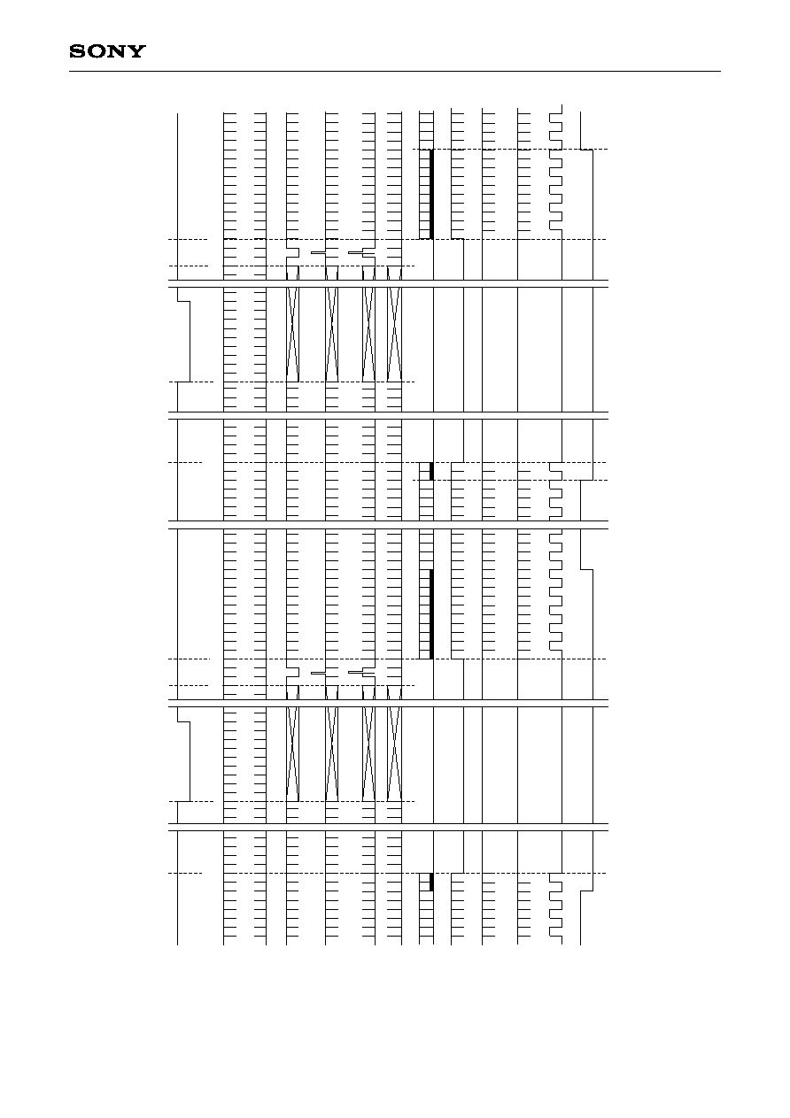
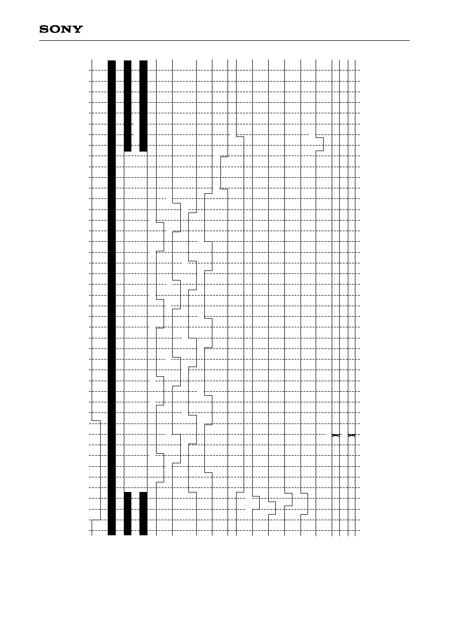
Char
t-1
V
e
r
tical Direction
Timing Char
t
MODE
Prog
ressiv
e scan mode
≠
high-speed s
w
eep not present
≠
28MHz (36MHz) driv
e
Applicab
le CCD ima
g
e sensor
∑
ICX274
The n
umber of SUB pulses is deter
mined b
y
the ser
ial interf
ace data.
This char
t sho
ws the case where SUB pulses are output in a
ll hor
i
z
ontal per
iods
.
ID/EXP of this char
t sho
ws ID
.
ID is lo
w f
or lines where CCD OUT contains the R component, and high f
or lines where CCD OUT con
tains the B component.
D
u
r
ing 28MHz dr
i
v
e
,
the
VR per
iod is 1493H, and at 1493H one hor
i
z
ontal per
iod is 1860c
k.
Dur
ing 36MHz dri
v
e
,
the
VR per
iod is 1252H, and at 1252H one hor
i
z
ontal per
iod is 480c
k.
VR
HR
SUB
V1
V2A/B/C
CCD OUT
PBLK
OBCLP
CLPDM
ID/EXP
WEN
V3A/B/C
V4
1
1251
1
1236
1235
1
2
3
4
5
6
7
8
9
10
1
2
3
4
5
6
7
8
9
10
1
2
3
4
5
6
7
8
9
10
1
2
3
4
5
6
7
8
9
10
1236
1235
1493 (1252)
1493 (1252)
A
A
3
1251
3

≠ 27 ≠
CXD3609R
Char
t-2
V
e
r
tical Direction
Timing Char
t
MODE
D
r
aft mode 28MHz (36MHz) dr
iv
e
Applicab
le CCD ima
g
e sensor
∑
ICX274
The n
umber of SUB pulses is deter
mined b
y
the ser
ial interf
ace data.
This char
t sho
ws the case where SUB pulses are output in a
ll hor
i
z
ontal per
iods
.
ID/EXP of this char
t sho
ws ID
.
ID is lo
w f
or lines where CCD OUT contains the R component, and high f
or lines where CCD OUT con
tains the B component.
D
u
r
ing 28MHz dr
iv
e
,
the
VR per
iod is 693H, and at 693H one hor
i
z
ontal per
iod is 810c
k.
Dur
ing 36MHz dr
iv
e
,
the
VR per
i
od is 871H, and at 871H one hor
i
z
ontal per
iod is 900c
k.
VR
HR
SUB
V1
V2C
CCD OUT
PBLK
OBCLP
CLPDM
ID/EXP
WEN
V2A/B
V3C
V3A/B
V4
693 (871)
693 (871)
1236
1235
5
6
9
10
3
4
7
8
1236
1235
1231
1232
5
6
9
10
3
4
7
8
A
624
624
2
2
A
1
1

≠ 28 ≠
CXD3609R
Char
t-3
V
e
r
tical Direction
Timing Char
t
MODE
Monitor
ing mode 28MHz (36MHz) dr
iv
e
Applicab
le CCD ima
g
e sensor
∑
ICX274
The n
umber of SUB pulses is deter
mined b
y
the ser
ial interf
ace data.
This char
t sho
ws the case where SUB pulses are output in a
ll hor
i
z
ontal per
iods
.
ID/EXP of this char
t sho
ws ID
.
ID is lo
w f
or lines where CCD OUT contains the R component, and high f
or lines where CCD OUT con
tains the B component.
D
u
r
ing 28MHz dr
iv
e
,
the
VR per
iod is 407H, and at 406H and 407H one hor
i
z
ontal per
iod is 1470c
k.
Dur
ing 36MHz dr
iv
e
,
the
VR per
i
od is 511H, and at 511H one hor
i
z
ontal per
iod is 1680c
k.
VR
HR
SUB
V1
V2A
CCD OUT
PBLK
OBCLP
CLPDM
ID/EXP
WEN
V2B/C
V3A
V3B/C
V4
407 (511)
407 (511)
1233
1230
3
8
1
6
9
14
17
22
25
1233
1230
3
8
1
6
9
14
17
22
25
1225
1225
A
313
313
2
2
A
1
1
≠ 29 ≠
CXD3609R
Char
t-4
V
e
r
tical Direction
Timing Char
t
MODE
Prog
ressiv
e scan mode
≠
high-speed s
w
eep present
≠
28MHz (36MHz) driv
e
Applicab
le CCD ima
g
e sensor
∑
ICX274
The n
umber of SUB pulses is deter
mined b
y
the ser
ial interf
ace data.
This char
t sho
ws the case where SUB pulses are output in a
ll hor
i
z
ontal per
iods
.
ID/EXP of this char
t sho
ws ID
.
ID is lo
w f
or lines where CCD OUT contains the R component, and high f
or lines where CCD OUT con
tains the B component.
D
u
r
ing 28MHz dr
i
v
e
,
the
VR per
iod is 1742H, and at 1742H one hor
i
z
ontal per
iod is 1530c
k.
Dur
ing 36MHz dr
i
v
e
,
the
VR per
iod is 1565H, and at 1564H and 1565H one hor
i
z
ontal per
iod is 1021c
k.
VR
HR
SUB
V1
V2A/B/C
CCD OUT
PBLK
OBCLP
CLPDM
ID/EXP
WEN
V3A/B/C
V4
1322
1236
1235
1
2
3
1
2
3
4
5
6
7
8
9
10
1236
1235
1
2
3
1
2
3
4
5
6
7
8
9
10
74
74
A
D
A
D
1742 (1565)
1742 (1565)
1322
71
71
1
1

≠ 30 ≠
CXD3609R
Char
t-5
V
e
r
tical Direction
Timing Char
t
MODE
Center scan 1 mode 28MHz dr
i
v
e
Applicab
le CCD ima
g
e sensor
∑
ICX274
The n
umber of SUB pulses is deter
mined b
y
the ser
ial interf
ace data.
This char
t sho
ws the case where SUB pulses are output in a
ll hor
i
z
ontal per
iods
.
ID/EXP of this char
t sho
ws ID
.
ID is lo
w f
or lines where CCD OUT contains the R component, and high f
or lines where CCD OUT con
tains the B component.
At 462H one hori
z
ontal per
iod is 1230c
k
.
VR
HR
SUB
V1
V2C
CCD OUT
PBLK
OBCLP
CLPDM
ID/EXP
WEN
V2A/B
V3C
V3A/B
V4
462
1055
188
191
192
195
1055
1052
460
452
16
18
462
460
452
16
18
188
191
192
195
A
DB
A
DB
1052
1
1
2
2

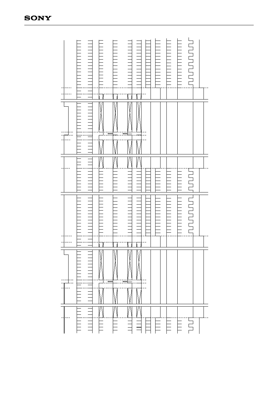
≠ 31 ≠
CXD3609R
Char
t-5.1
V
e
r
tical Direction
Timing Char
t
MODE
Center scan 1 mode 36MHz dr
i
v
e
Applicab
le CCD ima
g
e sensor
∑
ICX274
The n
umber of SUB pulses is deter
mined b
y
the ser
ial interf
ace data.
This char
t sho
ws the case where SUB pulses are output in a
ll hor
i
z
ontal per
iods
.
ID/EXP of this char
t sho
ws ID
.
ID is lo
w f
or lines where CCD OUT contains the R component, and high f
or lines where CCD OUT con
tains the B component.
At 581H one hor
iz
ontal per
iod is 601c
k.
VR
HR
SUB
V1
V2C
CCD OUT
PBLK
OBCLP
CLPDM
ID/EXP
WEN
V2A/B
V3C
V3A/B
V4
581
581
1188
1187
55
56
59
60
1188
1187
55
56
59
60
1184
1184
1183
1183
578
578
A
DB
A
DB
1
2
2
1
7
9
7
9
577
577

≠ 32 ≠
CXD3609R
Char
t-6
V
e
r
tical Direction
Timing Char
t
MODE
Center scan 2 mode 28MHz dr
i
v
e
Applicab
le CCD ima
g
e sensor
∑
ICX274
The n
umber of SUB pulses is deter
mined b
y
the ser
ial interf
ace data.
This char
t sho
ws the case where SUB pulses are output in a
ll hor
i
z
ontal per
iods
.
ID/EXP of this char
t sho
ws ID
.
ID is lo
w f
or lines where CCD OUT contains the R component, and high f
or lines where CCD OUT con
tains the B component.
At 462H one hori
z
ontal per
iod is 1230c
k
.
VR
HR
SUB
V1
V2C
CCD OUT
PBLK
OBCLP
CLPDM
ID/EXP
WEN
V2A/B
V3C
V3A/B
V4
188
191
192
195
1055
1053
1052
1050
186
189
190
193
188
191
192
195
1055
1053
1052
1050
186
189
190
193
1051
1049
1048
1046
DB
DB
1
454
462
16
18
454
16
18
462
1
2
2
A
A
≠ 33 ≠
CXD3609R
Char
t-6.1
V
e
r
tical Direction
Timing Char
t
MODE
Center scan 2 mode 36MHz dr
i
v
e
Applicab
le CCD ima
g
e sensor
∑
ICX274
The n
umber of SUB pulses is deter
mined b
y
the ser
ial interf
ace data.
This char
t sho
ws the case where SUB pulses are output in a
ll hor
i
z
ontal per
iods
.
ID/EXP of this char
t sho
ws ID
.
ID is lo
w f
or lines where CCD OUT contains the R component, and high f
or lines where CCD OUT con
tains the B component.
At 581H one hor
iz
ontal per
iod is 601c
k.
VR
HR
SUB
V1
V2C
CCD OUT
PBLK
OBCLP
CLPDM
ID/EXP
WEN
V2A/B
V3C
V3A/B
V4
1188
55
56
59
60
1186
1187
1185
1184
1182
1183
1181
53
54
57
58
55
56
59
60
53
54
57
58
1188
1186
1187
1185
1184
1182
1183
1181
A
DB
A
DB
578
581
7
9
578
9
581
1
7
2
2
1
577
577

≠ 34 ≠
CXD3609R
Char
t-7
V
e
r
tical Direction
Timing Char
t
MODE
Center scan 3 mode 28MHz dr
i
v
e
Applicab
le CCD ima
g
e sensor
∑
ICX274
The n
umber of SUB pulses is deter
mined b
y
the ser
ial interf
ace data.
This char
t sho
ws the case where SUB pulses are output in a
ll hor
i
z
ontal per
iods
.
ID/EXP of this char
t sho
ws ID
.
ID is lo
w f
or lines where CCD OUT contains the R component, and high f
or lines where CCD OUT con
tains the B component.
At 498H one hori
z
ontal per
iod is 1260c
k
.
VR
HR
SUB
V1
V2A/B/C
CCD OUT
PBLK
OBCLP
CLPDM
ID/EXP
WEN
V3A/B/C
V4
840
839
397
398
840
839
397
398
A
DB
D
B
1
479
498
33
35
1
497
35
479
497
33
2
2
A
498
≠ 35 ≠
CXD3609R
Char
t-7.1
V
e
r
tical Direction
Timing Char
t
MODE
Center scan 3 mode 36MHz dr
i
v
e
Applicab
le CCD ima
g
e sensor
∑
ICX274
The n
umber of SUB pulses is deter
mined b
y
the ser
ial interf
ace data.
This char
t sho
ws the case where SUB pulses are output in a
ll hor
i
z
ontal per
iods
.
ID/EXP of this char
t sho
ws ID
.
ID is lo
w f
or lines where CCD OUT contains the R component, and high f
or lines where CCD OUT con
tains the B component.
At 626H one hori
z
ontal per
iod is 1200c
k
.
VR
HR
SUB
V1
V2A/B/C
CCD OUT
PBLK
OBCLP
CLPDM
ID/EXP
WEN
V3A/B/C
V4
908
907
329
330
908
907
329
330
A
DB
A
DB
625
626
30
610
28
610
626
28
30
625
1
2
1
2
≠ 36 ≠
CXD3609R
Char
t-8
V
e
r
tical Direction
Timing Char
t
MODE
AF1 mode 28MHz dr
i
v
e
Applicab
le CCD ima
g
e sensor
∑
ICX274
The n
umber of SUB pulses is deter
mined b
y
the ser
ial interf
ace data.
This char
t sho
ws the case where SUB pulses are output in a
ll hor
i
z
ontal per
iods
.
ID/EXP of this char
t sho
ws ID
.
ID is lo
w f
or lines where CCD OUT contains the R component, and high f
or lines where CCD OUT con
tains the B component.
At 203H and 204H one hor
i
z
ontal per
iod is 1323c
k.
VR
HR
SUB
V1
V2A
CCD OUT
PBLK
OBCLP
CLPDM
ID/EXP
WEN
V2B/C
V3A
V3B/C
V4
958
286
289
953
958
286
289
953
A
DB
A
DB
204
202
191
20
22
204
202
191
20
22
1
2
2
1

≠ 37 ≠
CXD3609R
Char
t-8.1
V
e
r
tical Direction
Timing Char
t
MODE
AF1 mode 36MHz dr
i
v
e
Applicab
le CCD ima
g
e sensor
∑
ICX274
The n
umber of SUB pulses is deter
mined b
y
the ser
ial interf
ace data.
This char
t sho
ws the case where SUB pulses are output in a
ll hor
i
z
ontal per
iods
.
ID/EXP of this char
t sho
ws ID
.
ID is lo
w f
or lines where CCD OUT contains the R component, and high f
or lines where CCD OUT con
tains the B component.
At 256H one hor
iz
ontal per
iod is 840c
k.
VR
HR
SUB
V1
V2A
CCD OUT
WEN
V2B/C
V3A
V3B/C
V4
1089
153
158
1089
1086
153
158
1086
A
DB
A
DB
256
255
249
12
14
256
255
249
12
14
1
1
2
2
PBLK
OBCLP
CLPDM
ID/EXP

≠ 38 ≠
CXD3609R
Char
t-9
V
e
r
tical Direction
Timing Char
t
MODE
AF2 mode 28MHz dr
i
v
e
Applicab
le CCD ima
g
e sensor
∑
ICX274
The n
umber of SUB pulses is deter
mined b
y
the ser
ial interf
ace data.
This char
t sho
ws the case where SUB pulses are output in a
ll hor
i
z
ontal per
iods
.
ID/EXP of this char
t sho
ws ID
.
ID is lo
w f
or lines where CCD OUT contains the R component, and high f
or lines where CCD OUT con
tains the B component.
At 102H one hori
z
ontal per
iod is 1323c
k
.
VR
HR
SUB
V1
V2A
CCD OUT
PBLK
OBCLP
CLPDM
ID/EXP
WEN
V2B/C
V3A
V3B/C
V4
705
537
542
702
705
537
542
702
A
DB
A
DB
101
81
36
38
102
101
81
36
38
102
1
2
1
2

≠ 39 ≠
CXD3609R
Char
t-9.1
V
e
r
tical Direction
Timing Char
t
MODE
AF2 mode 36MHz dr
i
v
e
Applicab
le CCD ima
g
e sensor
∑
ICX274
The n
umber of SUB pulses is deter
mined b
y
the ser
ial interf
ace data.
This char
t sho
ws the case where SUB pulses are output in a
ll hor
i
z
ontal per
iods
.
ID/EXP of this char
t sho
ws ID
.
ID is lo
w f
or lines where CCD OUT contains the R component, and high f
or lines where CCD OUT con
tains the B component.
At 128H one hori
z
ontal per
iod is 1596c
k
.
PBLK
OBCLP
CLPDM
ID/EXP
VR
HR
SUB
V1
V2A
CCD OUT
WEN
V2B/C
V3A
V3B/C
V4
769
473
478
766
769
473
478
766
A
DB
A
DB
1
128
127
109
32
34
1
128
127
109
32
34
2
2

≠ 40 ≠
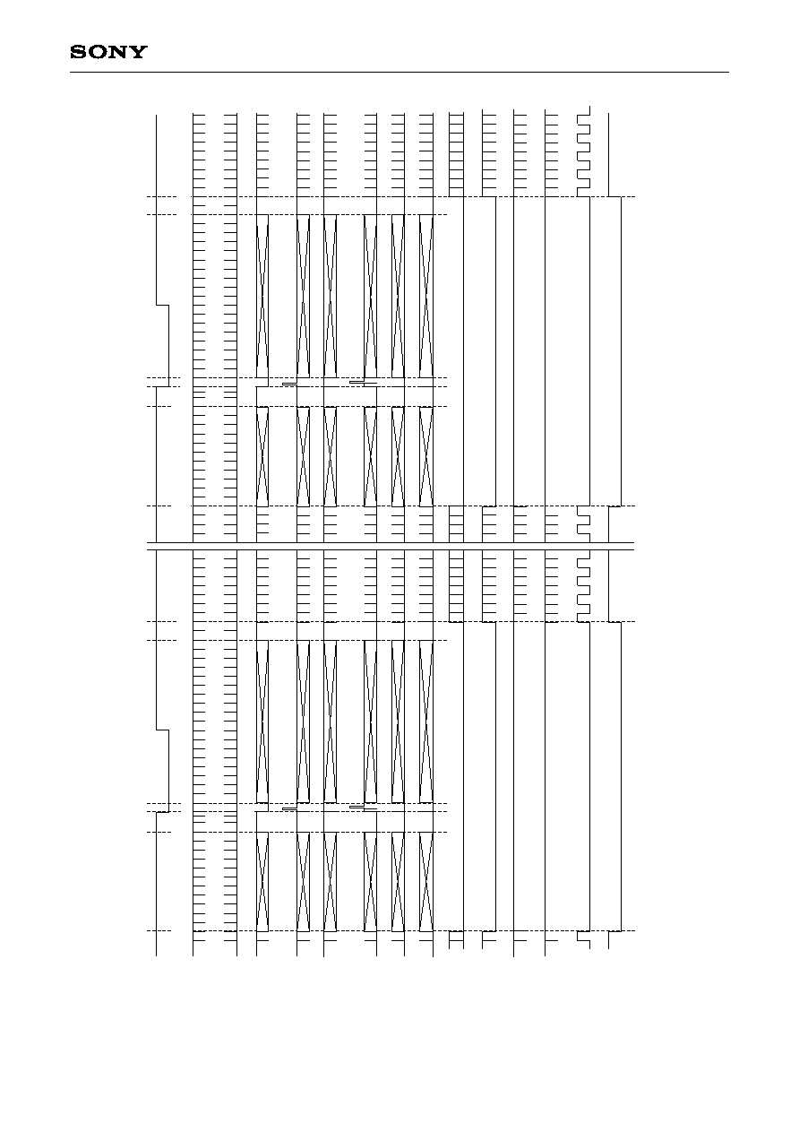
CXD3609R
Char
t-10
V
e
r
tical Direction
Timing Char
t
MODE
2-line addition mode 28MHz (36MHz) dr
iv
e
Applicab
le CCD ima
g
e sensor
∑
ICX274
The n
umber of SUB pulses is deter
mined b
y
the ser
ial interf
ace data.
This char
t sho
ws the case where SUB pulses are output in a
ll hor
i
z
ontal per
iods
.
ID/EXP of this char
t sho
ws ID
.
ID is lo
w f
or lines where CCD OUT contains the R component, and high f
or lines where CCD OUT con
tains the B component.
D
u
r
ing 28MHz dr
iv
e
,
the
VR per
iod is 693H, and at 693H one hor
i
z
ontal per
iod is 810c
k.
Dur
ing 36MHz dr
iv
e
,
the
VR per
i
od is 871H, and at 871H one hor
i
z
ontal per
iod is 900c
k.
PBLK
OBCLP
CLPDM
ID/EXP
VR
HR
SUB
V1
CCD OUT
WEN
V2A/B
V3A/B
V4
1
693 (871)
626
1
693 (871)
626
1236
5
6
9
10
1234
1235
1233
1232
1230
1231
1229
3
4
7
8
2
1
1236
5
6
9
10
1234
1235
1233
1232
1230
1231
1229
3
4
7
8
2
1
3
4
7
8
1
2
5
6
3
4
7
8
1
2
5
6
A
A
V2C
V3C
2
2

≠ 41 ≠
CXD3609R
Char
t-11
Horizontal Direction
Timing Char
t
MODE
Prog
ressiv
e scan mode
≠
high-speed s
w
eep present/not present
≠
28MHz (36MHz) dr
iv
e
Center scan 3 mode 28MHz (36MHz) dr
i
v
e
Applicab
le CCD ima
g
e sensor
∑
ICX274
The HR of this char
t indicates the actual CXD3609R load timing.
The n
umbers at the output pulse tr
ansition points indicate the count at the MCK
O
r
ise from the f
all of HR.
The HR f
all per
iod should be between appro
ximately 5.0 to 28.7µs (when the dr
i
v
e frequency is 28MHz).
This char
t sho
ws a per
iod of 185c
k (6.5µs).
The inter
nal SSG operates at this timing.
ID/EXP and
WEN are output at the timings sho
wn abo
v
e
at the v
e
r
tical positions sho
wn in Char
t-1 and Char
t-7.
HR
H1A/B
H2A/B
MCKO
V1
PBLK
OBCLP (1)
OBCLP (4)
V2A/B/C
V4
1920
0
CLPDM
300
100
200
400
70
124
106
160
52
142
V3A/B/C
88
178
SUB
187
247
52
256
296
284
52
284
OBCLP (2)
44
20
4
34
10
OBCLP (3)
50
26
10
50
158
282
ID/EXP
258
158
WEN
≠ 42 ≠
CXD3609R
Char
t-12
Horizontal Direction
Timing Char
t
MODE
Monitor
ing mode 28MHz (36MHz) dr
iv
e
AF1 and AF2 mode 28MHz (36MHz) dr
i
v
e
Applicab
le CCD ima
g
e sensor
∑
ICX274
The HR of this char
t indicates the actual CXD3609R load timing.
The n
umbers at the output pulse tr
ansition points indicate the count at the MCK
O
r
ise from the f
all of HR.
The HR f
all per
iod should be between appro
ximately 5.0 to 28.7µs (when the dr
i
v
e frequency is 28MHz).
This char
t sho
ws a per
iod of 185c
k (6.5µs).
The inter
nal SSG operates at this timing.
ID/EXP and
WEN are output at the timings sho
wn abo
v
e
at the v
e
r
tical positions sho
wn in Char
t-3, Char
t-8 and Char
t-9.
HR
H1A/B
H2A/B
MCKO
V1
PBLK
OBCLP (1)
OBCLP (4)
V2A/B/C
V4
CLPDM
V3A/B/C
SUB
OBCLP (2)
OBCLP (3)
ID/EXP
WEN
2352
0
600
200
400
800
70
214
88
178
688
728
716
52
716
44
20
4
34
10
50
26
10
50
158
714
690
158
100
300
500
700
52
124
268
358
412
502
556
106
250
160
304
394
448
538
592
142
286
196
340
430
484
574
232
322
376
466
520
610
52
619
679

≠ 43 ≠
CXD3609R
Char
t-13
Horizontal Direction
Timing Char
t
MODE
D
r
aft mode 28MHz (36MHz) dr
iv
e
2-line addition mode 28MHz (36MHz) dr
iv
e
Center scan 1 and center scan 2 mode 28MHz (36MHz) dr
i
v
e
Applicab
le CCD ima
g
e sensor
∑
ICX274
The HR of this char
t indicates the actual CXD3609R load timing.
The n
umbers at the output pulse tr
ansition points indicate the count at the MCK
O
r
ise from the f
all of HR.
The HR f
all per
iod should be between appro
ximately 5.0 to 28.7µs (when the dr
i
v
e frequency is 28MHz).
This char
t sho
ws a per
iod of 185c
k (6.5µs).
The inter
nal SSG operates at this timing.
ID/EXP and
WEN are output at the timings sho
wn abo
v
e
at the v
e
r
tical positions shown in Char
t-2, Char
t-5, Char
t-6 and Char
t-10.
HR
H1A/B
H2A/B
MCKO
V1
PBLK
OBCLP (1)
OBCLP (4)
V2A/B/C
V4
CLPDM
V3A/B/C
SUB
OBCLP (2)
OBCLP (3)
ID/EXP
WEN
2070
0
400
300
4
214
88
178
406
446
434
52
434
44
20
52
34
10
50
26
10
50
158
432
408
158
100
200
500
124
70
268
106
250
160
304
142
286
196
232
322
52
334
394

≠ 44 ≠
CXD3609R
Char
t-14
Horizontal Direction
Timing Char
t
(D:
high-speed s
weep)
MODE
Prog
ressiv
e scan mode
≠
high-speed s
w
eep present
≠
28MHz (36MHz) dr
iv
e
Applicab
le CCD ima
g
e sensor
∑
ICX274
The HR of this char
t indicates the actual CXD3609R load timing.
The n
umbers at the output pulse tr
ansition points indicate the count at the MCK
O
r
ise from the f
all of HR.
The HR f
all per
iod should be between appro
ximately 5.0 to 28.7µs (when the dr
i
v
e frequency is 28MHz).
This char
t sho
ws a per
iod of 185c
k (6.5µs).
The inter
nal SSG operates at this timing.
HR
V1
V4
1920
0
71H
1ck
1800
200
400
4
100
300
500
52
70
430
214
286
#1
#3
#2
#5
#4
52
124
196
142
268
340
358
412
#1865
#1864
106
88
160
178
250
232
322
304
394
376
466
448
1834
1834
1816
1816
1798
1798
1780
1780
1762
1762
1744
1744
1726
1726
502
484
70
430
214
286
52
124
196
142
268
340
358
412
106
88
160
178
250
232
322
304
394
376
466
448
502
484
256
284
296
4
52
#6
1708
1708
1888
1852
#1866
1906
1906
1888
1870
1870
1852
H1A/B
H2A/B
MCKO
V2A/B/C
V3A/B/C

≠ 45 ≠
CXD3609R
Char
t-15
Horizontal Direction
Timing Char
t
(D:
high-speed s
weep)
MODE
Center scan 1 and center scan 2 mode 28MHz dr
iv
e
Applicab
le CCD ima
g
e sensor
∑
ICX274
The HR of this char
t indicates the actual CXD3609R load timing.
The n
umbers at the output pulse tr
ansition points indicate the count at the MCK
O
r
ise from the f
all of HR.
The HR f
all per
iod should be between appro
ximately 5.0 to 28.7µs (when the dr
i
v
e frequency is 28MHz).
This char
t sho
ws a per
iod of 185c
k (6.5µs).
The inter
nal SSG operates at this timing.
HR
V1
V4
2070
0
460H or 462H
1
2000
1900
200
400
4
100
300
500
52
70
430
214
286
#1
#3
#2
#5
#4
52
124
196
142
268
340
358
412
#229
#228
106
88
160
178
250
232
322
304
394
376
466
448
2032
2014
1996
1978
1960
1942
1924
502
484
70
430
214
286
52
124
196
142
268
340
358
412
106
88
160
178
250
232
322
304
394
376
466
448
502
484
406
434
446
4
52
#6
1906
2032
2014
1996
1978
1960
1942
1924
1906
H1A/B
H2A/B
MCKO
V2A/B/C
V3A/B/C

≠ 46 ≠
CXD3609R
Char
t-15.1
Horizontal Direction
Timing Char
t
(D:
high-speed s
weep)
MODE
Center scan 1 and center scan 2 mode 36MHz dr
iv
e
Applicab
le CCD ima
g
e sensor
∑
ICX274
The HR of this char
t indicates the actual CXD3609R load timing.
The n
umbers at the output pulse tr
ansition points indicate the count at the MCK
O
r
ise from the f
all of HR.
The HR f
all per
iod should be between appro
ximately 5.0 to 28.7µs (when the dr
i
v
e frequency is 28MHz).
This char
t sho
ws a per
iod of 185c
k (6.5µs).
The inter
nal SSG operates at this timing.
HR
V1
V4
2070
0
581H
1 (2070)
2000
1900
200
400
4
100
300
500
52
70
430
214
286
#1
#3
#2
#5
#4
52
124
196
142
268
340
358
412
#85
#84
106
88
160
178
250
232
322
304
394
376
466
448
2014
1996
1978
1960
1942
1924
1906
502
484
70
430
214
286
52
124
196
142
268
340
358
412
106
88
160
178
250
232
322
304
394
376
466
448
502
484
406
434
446
4
52
#6
1870
2014
1996
1978
1960
1942
1924
1906
1870
H1A/B
H2A/B
MCKO
V2A/B/C
V3A/B/C

≠ 47 ≠
CXD3609R
Char
t-16
Horizontal Direction
Timing Char
t
(D:
high-speed s
weep)
MODE
Center scan 3 mode 28MHz dr
i
v
e
Applicab
le CCD ima
g
e sensor
∑
ICX274
The HR of this char
t indicates the actual CXD3609R load timing.
The n
umbers at the output pulse tr
ansition points indicate the count at the MCK
O
r
ise from the f
all of HR.
The HR f
all per
iod should be between appro
ximately 5.0 to 28.7µs (when the dr
i
v
e frequency is 28MHz).
This char
t sho
ws a per
iod of 185c
k (6.5µs).
The inter
nal SSG operates at this timing.
HR
V1
V4
1920
0
497H
1
1800
200
400
4
100
300
500
52
70
430
214
286
#1
#3
#2
#5
#4
52
124
196
142
268
340
358
412
#479
#478
106
88
160
178
250
232
322
304
394
376
466
448
1882
1864
1846
1828
1810
1792
1774
502
484
70
430
214
286
52
124
196
142
268
340
358
412
106
88
160
178
250
232
322
304
394
376
466
448
502
484
256
284
296
4
52
#6
1756
1882
1864
1846
1828
1810
1792
1774
1756
H1A/B
H2A/B
MCKO
V2A/B/C
V3A/B/C

≠ 48 ≠
CXD3609R
Char
t-16.1
Horizontal Direction
Timing Char
t
(D:
high-speed s
weep)
MODE
Center scan 3 mode 36MHz dr
i
v
e
Applicab
le CCD ima
g
e sensor
∑
ICX274
The HR of this char
t indicates the actual CXD3609R load timing.
The n
umbers at the output pulse tr
ansition points indicate the count at the MCK
O
r
ise from the f
all of HR.
The HR f
all per
iod should be between appro
ximately 5.0 to 28.7µs (when the dr
i
v
e frequency is 28MHz).
This char
t sho
ws a per
iod of 185c
k (6.5µs).
The inter
nal SSG operates at this timing.
HR
V1
V4
1920
0
625H
1
1800
200
400
4
100
300
500
52
70
430
214
286
#1
#3
#2
#5
#4
52
124
196
142
268
340
358
412
#399
#398
106
88
160
178
250
232
322
304
394
376
466
448
1882
1864
1846
1828
1810
1792
1774
502
484
70
430
214
286
52
124
196
142
268
340
358
412
106
88
160
178
250
232
322
304
394
376
466
448
502
484
256
284
296
4
52
#6
1756
1882
1864
1846
1828
1810
1792
1774
1756
H1A/B
H2A/B
MCKO
V2A/B/C
V3A/B/C

≠ 49 ≠
CXD3609R
Char
t-17
Horizontal Direction
Timing Char
t
(D:
high-speed s
weep)
MODE
AF1 mode
, 28MHz dr
i
v
e
Applicab
le CCD ima
g
e sensor
∑
ICX274
The HR of this char
t indicates the actual CXD3609R load timing.
The n
umbers at the output pulse tr
ansition points indicate the count at the MCK
O
r
ise from the f
all of HR.
The HR f
all per
iod should be between appro
ximately 5.0 to 28.7µs (when the dr
i
v
e frequency is 28MHz).
This char
t sho
ws a per
iod of 185c
k (6.5µs).
The inter
nal SSG operates at this timing.
HR
V1
V4
2352
0
202H
1
2200
2300
200
400
4
100
300
500
52
70
430
214
286
#1
#3
#2
#5
#4
52
124
196
142
268
340
358
412
#358
#357
106
88
160
178
250
232
322
304
394
376
466
448
2290
2272
2254
2236
2218
2200
2182
502
484
70
430
214
286
52
124
196
142
268
340
358
412
106
88
160
178
250
232
322
304
394
376
466
448
502
484
4
52
#6
2164
2290
2272
2254
2236
2218
2200
2182
2164
H1A/B
H2A/B
MCKO
V2A/B/C
V3A/B/C

≠ 50 ≠
CXD3609R
Char
t-17.1
Horizontal Direction
Timing Char
t
(D:
high-speed s
weep)
MODE
AF1 mode
, 36MHz dr
i
v
e
Applicab
le CCD ima
g
e sensor
∑
ICX274
The HR of this char
t indicates the actual CXD3609R load timing.
The n
umbers at the output pulse tr
ansition points indicate the count at the MCK
O
r
ise from the f
all of HR.
The HR f
all per
iod should be between appro
ximately 5.0 to 28.7µs (when the dr
i
v
e frequency is 28MHz).
This char
t sho
ws a per
iod of 185c
k (6.5µs).
The inter
nal SSG operates at this timing.
HR
V1
V4
2352
0
255H
1
2200
2300
200
400
4
100
300
500
52
70
430
214
286
#1
#3
#2
#5
#4
52
124
196
142
268
340
358
412
#195
#194
106
88
160
178
250
232
322
304
394
376
466
448
2314
2296
2278
2260
2242
2224
2206
502
484
70
430
214
286
52
124
196
142
268
340
358
412
106
88
160
178
250
232
322
304
394
376
466
448
502
484
4
52
#6
2188
2314
2296
2278
2260
2242
2224
2206
2188
H1A/B
H2A/B
MCKO
V2A/B/C
V3A/B/C
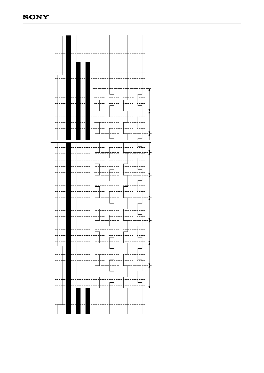
≠ 51 ≠
CXD3609R
Char
t-18
Horizontal Direction
Timing Char
t
(D:
high-speed s
weep)
MODE
AF2 mode
, 28MHz dr
i
v
e
Applicab
le CCD ima
g
e sensor
∑
ICX274
The HR of this char
t indicates the actual CXD3609R load timing.
The n
umbers at the output pulse tr
ansition points indicate the count at the MCK
O
r
ise from the f
all of HR.
The HR f
all per
iod should be between appro
ximately 5.0 to 28.7µs (when the dr
i
v
e frequency is 28MHz).
This char
t sho
ws a per
iod of 185c
k (6.5µs).
The inter
nal SSG operates at this timing.
HR
V1
V4
2352
0
101H
1
2200
2300
200
400
4
100
300
500
52
70
430
214
286
#1
#3
#2
#5
#4
52
124
196
142
268
340
358
412
#652
#651
106
88
160
178
250
232
322
304
394
376
466
448
2290
2272
2254
2236
2218
2200
2182
502
484
70
430
214
286
52
124
196
142
268
340
358
412
106
88
160
178
250
232
322
304
394
376
466
448
502
484
4
52
#6
2164
2290
2272
2254
2236
2218
2200
2182
2164
H1A/B
H2A/B
MCKO
V2A/B/C
V3A/B/C

≠ 52 ≠
CXD3609R
Char
t-18.1
Horizontal Direction
Timing Char
t
(D:
high-speed s
weep)
MODE
AF2 mode
, 36MHz dr
i
v
e
Applicab
le CCD ima
g
e sensor
∑
ICX274
The HR of this char
t indicates the actual CXD3609R load timing.
The n
umbers at the output pulse tr
ansition points indicate the count at the MCK
O
r
ise from the f
all of HR.
The HR f
all per
iod should be between appro
ximately 5.0 to 28.7µs (when the dr
i
v
e frequency is 28MHz).
This char
t sho
ws a per
iod of 185c
k (6.5µs).
The inter
nal SSG operates at this timing.
HR
V1
V4
2352
0
127H
1
2200
2300
200
400
4
100
300
500
52
70
430
214
286
#1
#3
#2
#5
#4
52
124
196
142
268
340
358
412
#587
#586
106
88
160
178
250
232
322
304
394
376
466
448
2314
2296
2278
2260
2242
2224
2206
502
484
70
430
214
286
52
124
196
142
268
340
358
412
106
88
160
178
250
232
322
304
394
376
466
448
502
484
4
52
#6
2188
2314
2296
2278
2260
2242
2224
2206
2188
H1A/B
H2A/B
MCKO
V2A/B/C
V3A/B/C

≠ 53 ≠
CXD3609R
Char
t-19
Horizontal Direction
Timing Char
t
(B: frame shift)
MODE
Center scan 1 and center scan 2 mode 28MHz dr
iv
e
Applicab
le CCD ima
g
e sensor
∑
ICX274
The HR of this char
t indicates the actual CXD3609R load timing.
The n
umbers at the output pulse tr
ansition points indicate the count at the MCK
O
r
ise from the f
all of HR.
The HR f
all per
iod should be between appro
ximately 5.0 to 28.7µs (when the dr
i
v
e frequency is 28MHz).
This char
t sho
ws a per
iod of 185c
k (6.5µs).
The inter
nal SSG operates at this timing.
HR
V1
V4
2070
0
15H
900
1000
200
400
4
100
300
500
52
106
394
844
#1
#3
#2
#194
#193
70
214
3
58
250
502
952
988
160
124
2
68
304
448
412
898
862
1042
1006
88
376
52
196
340
232
484
9
34
970
178
142
286
322
466
430
916
880
1060
1024
406
H1A/B
H2A/B
MCKO
V2A/B/C
V3A/B/C

≠ 54 ≠
CXD3609R
Char
t-19.1
Horizontal Direction
Timing Char
t
(B: frame shift)
MODE
Center scan 1 and center scan 2 mode 36MHz dr
iv
e
Applicab
le CCD ima
g
e sensor
∑
ICX274
The HR of this char
t indicates the actual CXD3609R load timing.
The n
umbers at the output pulse tr
ansition points indicate the count at the MCK
O
r
ise from the f
all of HR.
The HR f
all per
iod should be between appro
ximately 5.0 to 28.7µs (when the dr
i
v
e frequency is 28MHz).
This char
t sho
ws a per
iod of 185c
k (6.5µs).
The inter
nal SSG operates at this timing.
HR
V1
V4
2070
0
6H
400
500
200
400
4
100
300
500
52
106
3
94
322
#1
#3
#2
#61
#60
70
214
358
250
502
430
466
160
124
268
304
4
48
412
376
340
520
484
88
376
52
196
340
232
484
4
12
448
178
142
286
322
4
66
430
394
358
538
502
406
H1A/B
H2A/B
MCKO
V2A/B/C
V3A/B/C

≠ 55 ≠
CXD3609R
Char
t-20
Horizontal Direction
Timing Char
t
(B: frame shift)
MODE
Center scan 3 mode 28MHz dr
i
v
e
Applicab
le CCD ima
g
e sensor
∑
ICX274
The HR of this char
t indicates the actual CXD3609R load timing.
The n
umbers at the output pulse tr
ansition points indicate the count at the MCK
O
r
ise from the f
all of HR.
The HR f
all per
iod should be between appro
ximately 5.0 to 28.7µs (when the dr
i
v
e frequency is 28MHz).
This char
t sho
ws a per
iod of 185c
k (6.5µs).
The inter
nal SSG operates at this timing.
HR
V1
V4
1920
0
32H
900
1000
200
400
4
100
300
500
52
106
3
94
826
#1
#3
#2
#407
#406
214
3
58
250
502
934
970
160
124
268
304
4
48
412
880
844
1024
988
88
376
196
340
232
484
9
16
952
178
142
286
322
4
66
430
898
862
1042
1006
256
H1A/B
H2A/B
MCKO
V2A/B/C
V3A/B/C
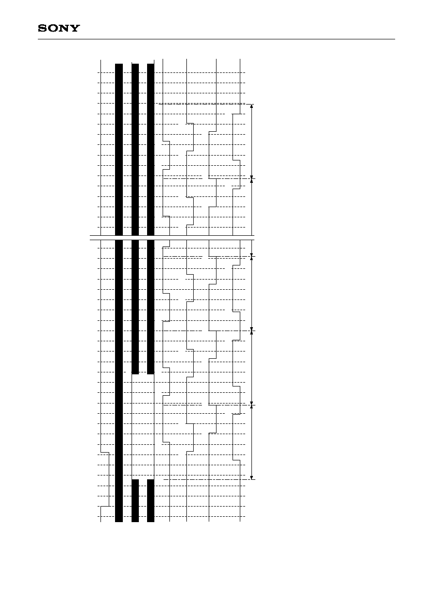
≠ 56 ≠
CXD3609R
Char
t-20.1
Horizontal Direction
Timing Char
t
(B: frame shift)
MODE
Center scan 3 mode 36MHz dr
i
v
e
Applicab
le CCD ima
g
e sensor
∑
ICX274
The HR of this char
t indicates the actual CXD3609R load timing.
The n
umbers at the output pulse tr
ansition points indicate the count at the MCK
O
r
ise from the f
all of HR.
The HR f
all per
iod should be between appro
ximately 5.0 to 28.7µs (when the dr
i
v
e frequency is 28MHz).
This char
t sho
ws a per
iod of 185c
k (6.5µs).
The inter
nal SSG operates at this timing.
HR
V1
V4
1920
0
27H
900
1000
200
400
4
100
300
500
52
106
3
94
634
#1
#3
#2
#339
#338
214
3
58
250
502
742
778
160
124
268
304
4
48
412
688
652
832
796
88
376
196
340
232
484
7
24
760
178
142
286
322
4
66
430
706
670
850
814
256
H1A/B
H2A/B
MCKO
V2A/B/C
V3A/B/C
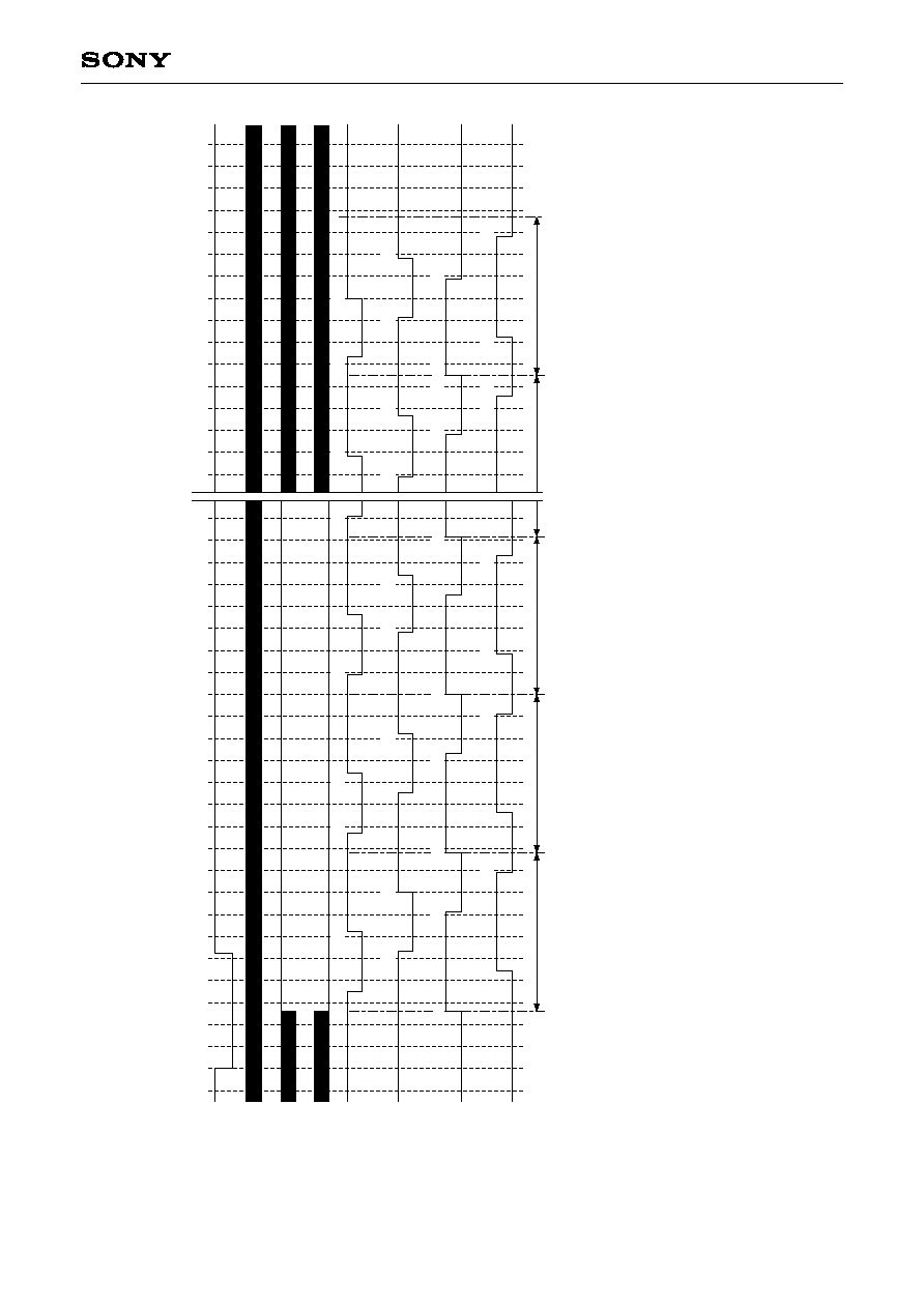
≠ 57 ≠
CXD3609R
Char
t-21
Horizontal Direction
Timing Char
t
(B: frame shift)
MODE
AF1 mode
, 28MHz dr
i
v
e
Applicab
le CCD ima
g
e sensor
∑
ICX274
The HR of this char
t indicates the actual CXD3609R load timing.
The n
umbers at the output pulse tr
ansition points indicate the count at the MCK
O
r
ise from the f
all of HR.
The HR f
all per
iod should be between appro
ximately 5.0 to 28.7µs (when the dr
i
v
e frequency is 28MHz).
This char
t sho
ws a per
iod of 185c
k (6.5µs).
The inter
nal SSG operates at this timing.
HR
V1
V4
2352
0
19H
1800
1900
200
400
4
100
300
500
52
106
394
1738
#1
#3
#2
#291
#290
70
214
358
250
502
1846
1882
160
124
268
304
448
412
1792
1756
1936
1900
88
376
52
196
340
232
484
1828
1864
178
142
286
322
466
430
1810
1774
1954
1918
H1A/B
H2A/B
MCKO
V2A/B/C
V3A/B/C
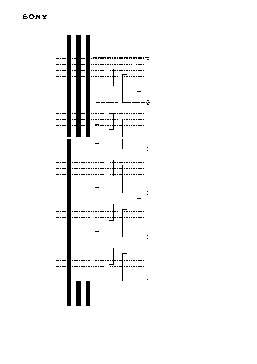
≠ 58 ≠
CXD3609R
Char
t-21.1
Horizontal Direction
Timing Char
t
(B: frame shift)
MODE
AF1 mode
, 36MHz dr
i
v
e
Applicab
le CCD ima
g
e sensor
∑
ICX274
The HR of this char
t indicates the actual CXD3609R load timing.
The n
umbers at the output pulse tr
ansition points indicate the count at the MCK
O
r
ise from the f
all of HR.
The HR f
all per
iod should be between appro
ximately 5.0 to 28.7µs (when the dr
i
v
e frequency is 28MHz).
This char
t sho
ws a per
iod of 185c
k (6.5µs).
The inter
nal SSG operates at this timing.
HR
V1
V4
2352
0
11H
1600
1700
200
400
4
100
300
500
52
106
394
1546
#1
#3
#2
#159
#158
70
214
358
250
502
1654
1690
160
124
268
304
448
412
1600
1564
1744
1708
88
376
52
196
340
232
484
1636
1672
178
142
286
322
466
430
1618
1582
1762
1726
H1A/B
H2A/B
MCKO
V2A/B/C
V3A/B/C

≠ 59 ≠
CXD3609R
Char
t-22
Horizontal Direction
Timing Char
t
(B: frame shift)
MODE
AF2 mode
, 28MHz dr
i
v
e
Applicab
le CCD ima
g
e sensor
∑
ICX274
The HR of this char
t indicates the actual CXD3609R load timing.
The n
umbers at the output pulse tr
ansition points indicate the count at the MCK
O
r
ise from the f
all of HR.
The HR f
all per
iod should be between appro
ximately 5.0 to 28.7µs (when the dr
i
v
e frequency is 28MHz).
This char
t sho
ws a per
iod of 185c
k (6.5µs).
The inter
nal SSG operates at this timing.
HR
V1
V4
2352
0
33H
500
600
200
400
4
100
300
500
52
106
394
394
#1
#3
#2
#543
#542
70
214
358
250
502
502
538
160
124
268
304
448
412
448
412
592
556
88
376
52
196
340
232
484
484
520
178
142
286
322
466
430
466
430
610
574
H1A/B
H2A/B
MCKO
V2A/B/C
V3A/B/C
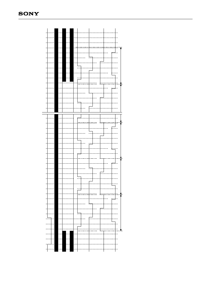
≠ 60 ≠
CXD3609R
Char
t-22.1
Horizontal Direction
Timing Char
t
(B: frame shift)
MODE
AF2 mode
, 36MHz dr
i
v
e
Applicab
le CCD ima
g
e sensor
∑
ICX274
The HR of this char
t indicates the actual CXD3609R load timing.
The n
umbers at the output pulse tr
ansition points indicate the count at the MCK
O
r
ise from the f
all of HR.
The HR f
all per
iod should be between appro
ximately 5.0 to 28.7µs (when the dr
i
v
e frequency is 28MHz).
This char
t sho
ws a per
iod of 185c
k (6.5µs).
The inter
nal SSG operates at this timing.
HR
V1
V4
2352
0
31H
600
700
800
200
400
4
100
300
500
52
106
394
586
#1
#3
#2
#479
#478
70
214
358
250
502
694
730
160
124
268
304
448
412
640
604
784
748
88
376
52
196
340
232
484
676
712
178
142
286
322
466
430
658
622
802
766
H1A/B
H2A/B
MCKO
V2A/B/C
V3A/B/C

≠ 61 ≠
CXD3609R
Char
t-23
Horizontal Direction
Timing Char
t
(A:
readout b
loc
k)
MODE
Prog
ressiv
e scan mode
≠
high-speed s
w
eep not present
≠
28MHz (36MHz) dr
iv
e
Applicab
le CCD ima
g
e sensor
∑
ICX274
The HR of this char
t indicates the actual CXD3609R load timing.
The n
umbers at the output pulse tr
ansition points indicate the count at the MCK
O
r
ise from the f
all of HR.
HR
V1
V2A/B/C
V4
1920
1
1920
1
V3A/B/C
SUB
282
342
282
342
70
124
106
1
60
52
142
1
96
88
178
214
1100
1250
70
106
124
52
88
142

≠ 62 ≠
CXD3609R
Char
t-24
Horizontal Direction
Timing Char
t
(A:
readout b
loc
k)
MODE
Monitor
ing mode 28MHz (36MHz) dr
iv
e
Applicab
le CCD ima
g
e sensor
∑
ICX274
The HR of this char
t indicates the actual CXD3609R load timing.
The n
umbers at the output pulse tr
ansition points indicate the count at the MCK
O
r
ise from the f
all of HR.
HR
V1
V2A
V4
2352
1
2352
1
V3A
SUB
V2B/C
V3B/C
282
342
70
124
106
160
52
142
88
178
214
268
250
304
196
286
232
322
358
412
394
448
340
430
376
466
502
556
538
592
484
574
520
610
646
628
1100
1250
1322
1412
1466
1556
1376
1430
1520
1394
1484
1538
1340
1358
1448
1502
70
124
106
160
52
142
88
178
214
268
250
304
196
286
232
322
358
412
394
448
336
426
376
466
502
556
538
592
480
570
520
610
619
679

≠ 63 ≠
CXD3609R
Char
t-25
Horizontal Direction
Timing Char
t
(A:
readout b
loc
k)
MODE
D
r
aft mode 28MHz (36MHz) dr
iv
e
Applicab
le CCD ima
g
e sensor
∑
ICX274
The HR of this char
t indicates the actual CXD3609R load timing.
The n
umbers at the output pulse tr
ansition points indicate the count at the MCK
O
r
ise from the f
all of HR.
HR
V1
V2C
V4
1920
1
V3C
SUB
V2A/B
V3A/B
70
124
106
160
52
142
88
178
214
268
250
304
196
2
86
232
322
358
340
334
394
1920
1
70
124
106
160
52
142
88
178
214
2
68
250
304
196
2
86
232
322
358
340
334
394
600
840
822
876
858
804
894
930
984
966
1020
912
1002
948
1038
1056
1074
750
1332
1314
1368
1350
1296
1386
1422
1476
1458
1512
1404
1494
1440
1530

≠ 64 ≠
CXD3609R
Char
t-26
Horizontal Direction
Timing Char
t
(A:
readout b
loc
k)
MODE
2-line addition mode 28MHz (36MHz) dr
iv
e
Applicab
le CCD ima
g
e sensor
∑
ICX274
The HR of this char
t indicates the actual CXD3609R load timing.
The n
umbers at the output pulse tr
ansition points indicate the count at the MCK
O
r
ise from the f
all of HR.
HR
V1
V2C
V4
1920
1
V3C
SUB
V2A/B
V3A/B
70
124
106
160
52
142
88
178
214
268
250
304
196
286
232
322
358
340
334
394
1920
1
70
124
106
160
52
142
88
178
214
268
250
304
196
286
232
322
358
340
334
394
600
840
822
876
858
804
894
930
984
966
1020
912
1002
948
1038
1056
1074
750
1128
1278
1332
1314
1368
1350
1296
1386
1422
1476
1458
1512
1404
1494
1440
1530

≠ 65 ≠
CXD3609R
Char
t-27
Horizontal Direction
Timing Char
t
(A:
readout b
loc
k)
MODE
Center scan 1 mode 28MHz (36MHz) dr
i
v
e
Applicab
le CCD ima
g
e sensor
∑
ICX274
The HR of this char
t indicates the actual CXD3609R load timing.
The n
umbers at the output pulse tr
ansition points indicate the count at the MCK
O
r
ise from the f
all of HR.
HR
V1
V2C
V4
2070
1
2070
1
V3C
SUB
V2A/B
V3A/B
70
124
106
160
52
142
88
178
214
268
250
304
196
286
232
322
358
340
334
390
70
124
106
160
52
142
88
178
214
268
250
304
196
286
232
322
358
340
334
390
600
840
822
876
858
804
894
930
984
966
1020
912
1002
948
1038
1056
1074
750
1128
1110
1164
1146
1092
1182
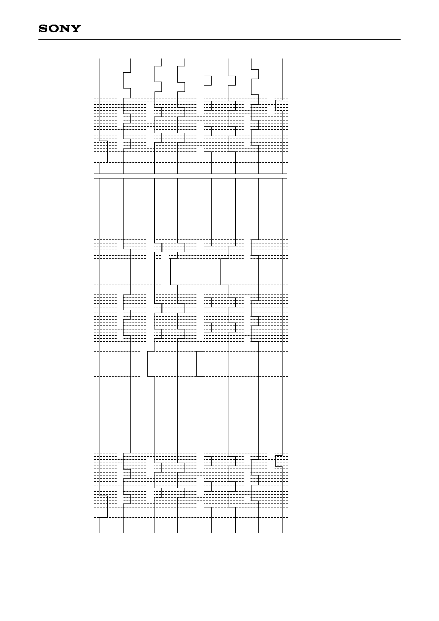
≠ 66 ≠
CXD3609R
Char
t-28
Horizontal Direction
Timing Char
t
(A:
readout b
loc
k)
MODE
Center scan 2 mode 28MHz (36MHz) dr
i
v
e
Applicab
le CCD ima
g
e sensor
∑
ICX274
The HR of this char
t indicates the actual CXD3609R load timing.
The n
umbers at the output pulse tr
ansition points indicate the count at the MCK
O
r
ise from the f
all of HR.
HR
V1
V2C
V4
2070
1
2070
1
V3C
SUB
V2A/B
V3A/B
70
124
106
160
52
142
88
178
214
268
250
304
196
286
232
322
358
340
334
390
70
124
106
160
52
142
88
178
214
268
250
304
196
286
232
322
358
340
334
390
600
840
822
876
858
804
894
930
984
966
1020
912
1002
948
1038
1056
1074
750
1332
1314
1368
1128
1278
1350
1296
1386
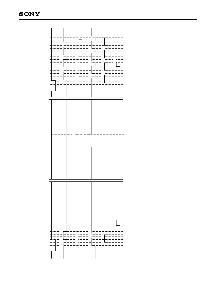
≠ 67 ≠
CXD3609R
Char
t-29
Horizontal Direction
Timing Char
t
(A:
readout b
loc
k)
MODE
Center scan 3 mode 28MHz (36MHz) dr
i
v
e
Applicab
le CCD ima
g
e sensor
∑
ICX274
The HR of this char
t indicates the actual CXD3609R load timing.
The n
umbers at the output pulse tr
ansition points indicate the count at the MCK
O
r
ise from the f
all of HR.
HR
V1
V2A/B/C
V4
1920
1
1920
1
V3A/B/C
SUB
282
342
282
342
70
124
106
160
52
142
196
88
178
214
1100
1250
106
142
196
268
340
430
484
160
250
304
394
448
88
124
214
268
358
412
178
232
322
376
466

≠ 68 ≠
CXD3609R
Char
t-30
Horizontal Direction
Timing Char
t
(A:
readout b
loc
k)
MODE
AF1 and AF2 mode 28MHz (36MHz) dr
i
v
e
Applicab
le CCD ima
g
e sensor
∑
ICX274
The HR of this char
t indicates the actual CXD3609R load timing.
The n
umbers at the output pulse tr
ansition points indicate the count at the MCK
O
r
ise from the f
all of HR.
HR
V1
V2A
V4
2352
1
2352
1
V3A
SUB
V2B/C
V3B/C
619
679
70
124
106
160
52
142
88
178
214
268
250
304
196
286
232
322
358
412
394
448
340
430
376
466
502
556
538
592
484
574
520
610
646
628
1100
1250
1322
1412
1466
1556
1610
1700
1376
1430
1520
1574
1664
1394
1484
1538
1628
1682
1340
1358
1448
1502
1592
1646
70
124
106
160
52
142
88
178
214
268
250
304
196
286
232
322
358
412
394
448
336
426
376
466
502
556
538
592
480
570
520
610
619
679

≠ 69 ≠
CXD3609R
Char
t-31
High-Speed Phase
Timing Char
t
MODE
Applicab
le CCD ima
g
e sensor
∑
ICX274
HR' of this char
t indicates the actual CXD3606R load timing.
The phase relationship of each pulse sho
ws the logical position relationship
.
F
or the actual output w
a
v
e
f
o
r
m, a dela
y is added
to each pulse
.
The logic phase of ADCLK can be specified b
y
the ser
ial interf
ace data.
HR
ADCLK
MCKO
XSHD
RG
HR'
CKI
CKO
XSHP
H1A/B
H2A/B
256/406/688
1
52

≠ 70 ≠
CXD3609R
Char
t-32
V
e
r
tical Direction Sequence Char
t
MODE
Prog
ressiv
e scan mode
≠
high-speed s
w
eep not present
≠
28MHz (36MHz) driv
e
T
r
igger in mode
T
r
igger
mode
T
r
igger out mode
Applicab
le CCD ima
g
e sensor
∑
ICX274
The n
umber of SUB pulses is deter
mined b
y
the ser
ial interf
ace data.
This char
t sho
ws the case where SUB pulses are output in a
ll hor
i
z
ontal per
iods
.
ID/EXP of this char
t sho
ws ID
.
ID is lo
w f
or lines where CCD OUT contains the R component, and high f
or lines where CCD OUT con
tains the B component.
D
u
r
ing 28MHz dr
i
v
e
,
the
VR per
iod is 1493H, and at 1493H one hor
i
z
ontal per
iod is 1860c
k.
Dur
ing 36MHz dri
v
e
,
the
VR per
iod is 1252H, and at 1252H one hor
i
z
ontal per
iod is 480c
k.
The
VD f
all is not accepted until 2H after SG generation.
F
or e
xample
, when SG is generated at 23H,
VR is not accepted from 1H
to 24H, b
ut is accepted from 25H onw
ard.
Ev
en when SG gener
ation position > n
umber of SUB pulses in the ser
ial data, SG gener
ation position = number of SUB pulses is us
ed.
VR
HR
SUB
V1
V2A/B/C
CCD OUT
PBLK
OBCLP
CLPDM
ID/EXP
WEN
V3A/B/C
V4
1
1251
1
123456789
10
123456789
10
1493 (1252)
1493 (1252)
TRIG
All pixels
TRIG
TRIG-OUT
1236
1235
TRIG-IN
VD fall is not accepted until 2H after SG generation
(71)
(1)
High-speed sweep existent/
not existent setting
Number of SUB lines (ex. 75 lines, 72 to 4096 lines)
SG generation position setting (ex. 85H, 72H, to 4096H)
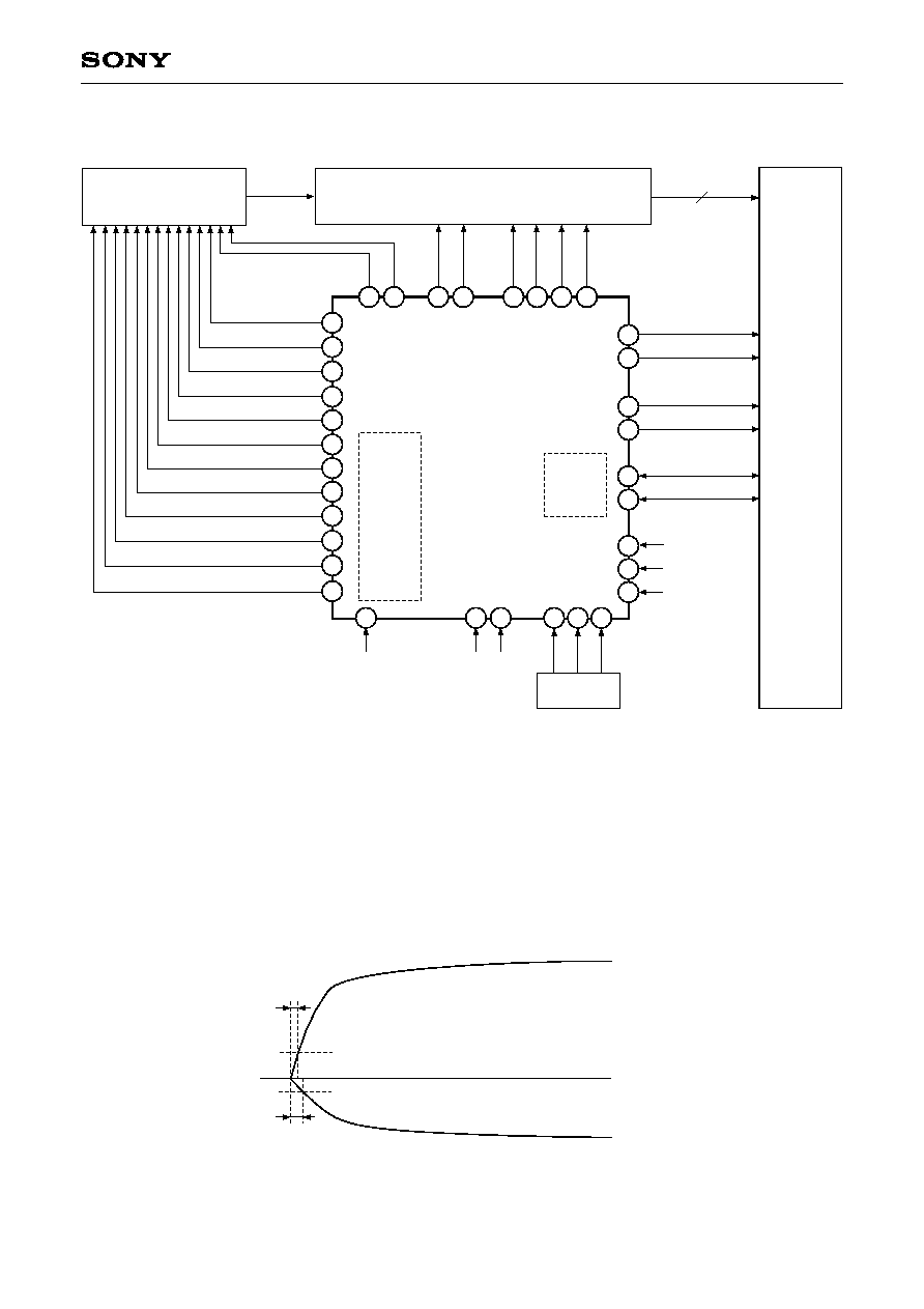
≠ 71 ≠
CXD3609R
Application Circuit Block diagram
Notes for Power-on
Of the three ≠7.5V, +15.0V, +3.3V power supplies, be sure to start up the ≠7.5V and +15.0V power supplies in
the following order to prevent the SUB pin of the CCD image sensor from going to negative potential.
Application circuits shown are typical examples illustrating the operation of the devices. Sony cannot assume responsibility for
any problems arising out of the use of these circuits or for any infringement of third party patent and other right due to same.
26
31 32
34
35
30
25
23
22
21
20
19
18
MCKO
VR
HR
CKO
Digital OUT
ADCLK
OBCLP
CLPDM
PBLK
XSHD
XSHP
15
13
SCK
33
SEN
SSI
CKI
27
TEST
28
TRIG
CCD OUT
V-Dr
SSG
5
4
WEN
ID/EXP
6
3
2
SSGSL
SNCSL
RST
H1A
10
12
H1B
H2A
H2B
8
RG
38
39
40
V2A
V4
V1
42
43
44
V3A
46
47
V3B
V3C
48
SUB
V2C
V2B
CCD
ICX274
CDS/ADC Block
Signal
Processor
Block
TG
CXD3609R
Controller
t1
t2
+15.0V
0V
≠7.5V
20%
20%
t2
t1

≠ 72 ≠
CXD3609R
Package Outline Unit: mm
Sony Corporation
SONY CODE
EIAJ CODE
JEDEC CODE
PACKAGE MATERIAL
LEAD TREATMENT
LEAD MATERIAL
PACKAGE MASS
EPOXY RESIN
COPPER ALLOY
PACKAGE STRUCTURE
48PIN LQFP (PLASTIC)
9.0 ± 0.2
7.0 ± 0.1
1
12
13
24
25
36
37
48
(0.22)
0.18 ≠ 0.03
+ 0.08
0.2g
LQFP-48P-L01
LQFP048-P-0707
(8.0)
0.5 ±
0.2
0.127 ≠ 0.02
+ 0.05
A
1.5 ≠ 0.1
+ 0.2
0.1
PALLADIUM PLATING
NOTE: Dimension "
" does not include mold protrusion.
0.1 ± 0.1
0.5 ±
0.2
0∞ to 10∞
DETAIL A
0.13 M
0.5
S
S
B
DETAIL B:PALLADIUM
0.127 ±
0.04
0.18 ± 0.03