--1--
E95444A57-TE
CXG1012N
High-Frequency SPDT Antenna Switch
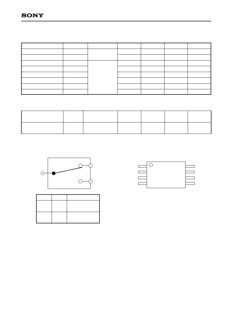
SSOP-8P-L01 (Plastic)
Absolute Maximum Ratings (Ta=25 ∞C)
∑ Control voltage
Vctl
6
V
∑ Operating temperature
Topr
≠35 to +85
∞C
∑ Storage temperature
Tstg
≠65 to +150
∞C
Operating Condition
Control voltage
0/3
V
Description
The CXG1012N is an antenna switch MMIC. This
IC is designed using the Sony's GaAs J-FET process
and operates at a single positive power supply.
Features
∑ Single positive power supply operation
∑ Insertion loss
0.5 dB (Typ.) at 2.0 GHz
∑ Medium power switching
P1dB (Typ.)
29 dBm
at 2.0 GHz
V
CTL
(H)=3.0V
33 dBm
at 2.0 GH
Z
V
CTL
(H)=4.0 V
Application
Antenna switch for digital cordless telephones
Structure
GaAs J-FET MMIC
Sony reserves the right to change products and specifications without prior notice. This information does not convey any license by
any implication or otherwise under any patents or other right. Application circuits shown, if any, are typical examples illustrating the
operation of the devices. Sony cannot assume responsibility for any problems arising out of the use of these circuits.
For the availability of this product, please contact the sales office.
--3--
CXG1012N
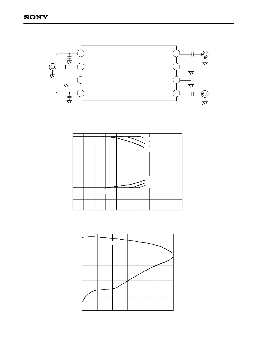
Recommended Circuit
Example of Representative Characteristics (Ta=25 ∞C)
100pF
100pF
CTLB
Port1
CTLA
Port3
Port2
100pF
100pF
100pF
CXG1012N
1
2
3
4
5
6
7
8
0
≠2
≠4
≠6
0
≠10
≠20
≠30
20
24
28
36
32
40
Insertion loss (dB)
Isolation (dB)
V
CTL
(H) =3V
V
CTL
(H) =4V
V
CTL
(H) =5V
V
CTL
(H) =3
V
V
CTL
(H) =4V
V
CTL
(H) =5V
Insertion loss
3
2
1
0
≠5
≠4
≠3
≠2
≠1
0
≠50
≠40
≠30
≠20
≠10
0
Frequency (GHz)
Insertion loss (dB)
Isolation (dB)
Insertion loss, isolation vs. Frequency
Insertion loss
Isolation
Insertion loss, isolation vs. Input power
Input power (dBm)
Isolation