--1--
E96526-TE
Sony reserves the right to change products and specifications without prior notice. This information does not convey any license by
any implication or otherwise under any patents or other right. Application circuits shown, if any, are typical examples illustrating the
operation of the devices. Sony cannot assume responsibility for any problems arising out of the use of these circuits.
High-Frequency SPDT Antenna Switch
CXG1024N
Absolute Maximum Ratings (Ta=25 ∞C)
∑ Supply voltage
V
DD
8
V
∑ Control voltage
Vctl (H)≠Vctl (L)
8
V
∑ Operating temperature Topr
≠35 to +85
∞C
∑ Storage temperature
Tstg
≠65 to +150
∞C
∑ Input Power
Pin (RF2, RF3, RF4) 37
dBm
Pin (RF1, RF5, RF6) 30
dBm
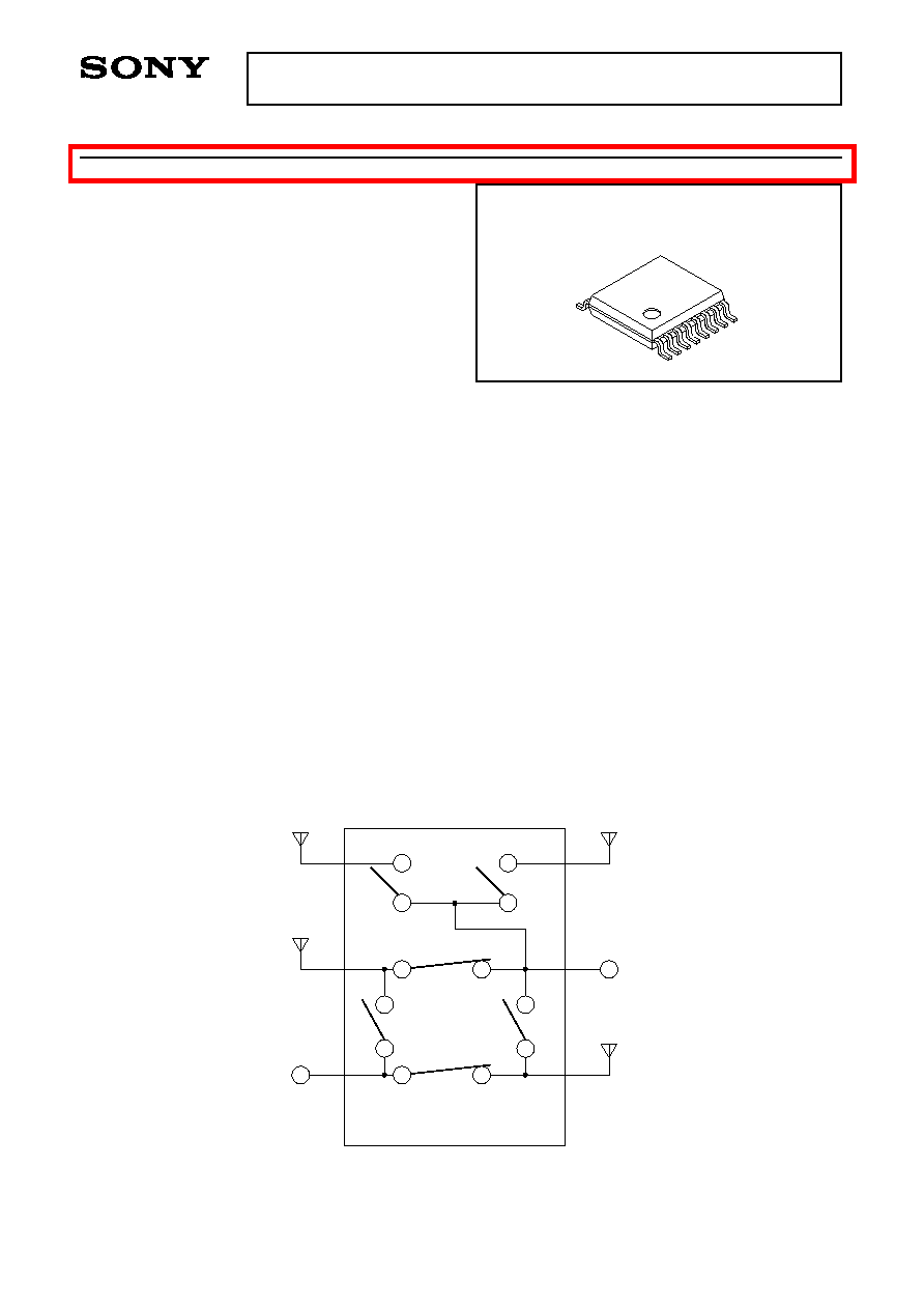
Description
The CXG1024N is a high power antenna switch
MMIC to connect T
X
/R
X
to one of 4 antennas. This
IC is designed using the Sony's GaAs J-FET
process and operates at a single positive power
supply.
Features
∑ Single positive power supply operation
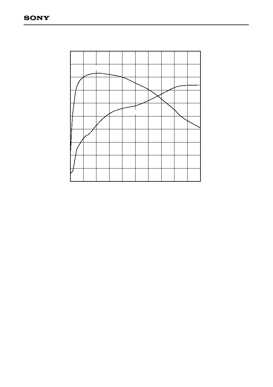
∑ Low insertion loss
0.4 dB (Typ.)
at 1.0 GHz
(T
X
Port)
∑ Isolation
21 dB (Typ.)
at 1.0 GHz
(T
X
Port)
∑ High power switching
P1 dB (Typ.)
32 dBm
at 1.5 GHz
V
CTL
(H)=3.0 V
35 dBm
at 1.5 GHz
V
CTL
(H)=4.0 V
Applications
Antenna switch for digital cellular telephones
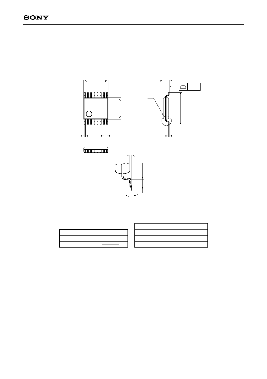
Structure
GaAs J-FET MMIC
16 pin SSOP (Plastic)
Function Block Diagram
Diversity Antenna 2
Diversity Antenna 1
Antenna 2
Antenna 1
T
X
R
X
For the availability of this product, please contact the sales office.
--2--
CXG1024N
Pin Configuration and Recommended Circuit
RF1
CTLC
V
DD
RF2
GND
CTLB
RF3
GND
RF6
CTLD
GND
RF5
GND
CTLA
RF4
GND
100pF
1
100pF
100pF
100pF
100pF
100k
8
CTLB
CTLA
CTLD
CTLC
CTLA
CTLB
16
9
100pF
100pF
100PF
100pF
100pF
100k
100pF
Logic Table
ON-Port
RF3≠RF2
RF3≠RF4
RF5≠RF2
RF5≠RF4
RF5≠RF6
RF5≠RF1
CTLA
H
L
L
H
L
L
CTLB
L
H
H
L
L
L
CTLC
H or L
H or L
L
L
L
H
CTLD
H or L
H or L
L
L
H
L
Recommended Operating Conditions
Item
Control Voltage (high)
Control Voltage (low)
Difference of Control Voltage
Supply voltage
Symbol
Vctl (H)
Vctl (L)
Vctl (H)≠Vctl (L)
V
DD
Min.
≠6
Vctl (H)≠0.6
Typ.
Vctl (H)≠0.5
Max.
6
6
Vctl (H)≠0.4
--3--
CXG1024N
Electrical Characteristics
(Ta=25 ∞C)
Insertion Loss
Isolation
VSWR
1 dB
Compression
Power
Switching Time
Control Current
Supply Current
Symbol
IL.
ISO.
VS.
P1 dB
t
SW
Ictl
I
DD
Signal
Passes
RF3≠RF2
RF3≠RF4
RF5≠RF2
RF5≠RF4
RF5≠RF1
RF5≠RF6
RF3≠RF2
RF3≠RF4
RF5≠RF2
RF5≠RF4
RF5≠RF1
RF5≠RF6
RF3≠RF2
RF3≠RF4
RF5≠RF2
RF5≠RF4
RF5≠RF1
RF5≠RF6
RF3≠RF2
RF3≠RF4
RF5≠RF2
RF5≠RF4
RF5≠RF1
RF5≠RF6
Test
Condition
2
Pin=30 dBm
2
Pin=20 dBm
2
Pin=20 dBm
2
Pin=20 dBm
2
Pin=30 dBm
2
Pin=20 dBm
2
Pin=30 dBm
2
Pin=20 dBm
3
2
1
3
2
1
2
2
Frequency
1 GHz
1.5 GHz
2 GHz
1 GHz
1.5 GHz
2 GHz
1 GHz
1.5 GHz
2 GHz
1 GHz
1.5 GHz
2 GHz
1 GHz
1.5 GHz
2 GHz
1 GHz
1.5 GHz
2 GHz
0.1 to 2 GHz
0.1 to 2 GHz
1.5 GHz
1.5 GHz
1.5 GHz
1.5 GHz
1.5 GHz
1.5 GHz
0.1 to 2 GHz
Min.
Typ.
Max.
Unit
0.4
0.65
0.5
0.8
0.7
1.0
0.5
0.8
0.65
0.95
0.9
1.2
dB
0.6
0.9
0.75
1.05
1.2
1.5
0.4
0.7
0.5
0.8
0.7
1.0
18
21
15
18
12
15
dB
21
24
17
20
15
18
1.3
1.5
1.3
1.5
30
32
33
35
35
37
dBm
22
24
25
27
27
29
200
nsec
µA
100
µA
100
1 : Vctl (H)=5 V, Vctl (L)=0 V, V
DD
=4.5 V
3 : Vctl (H)=3 V, Vctl (L)=0 V, V
DD
=2.5 V
2 : Vctl (H)=4 V, Vctl (L)=0 V, V
DD
=3.5 V