--1--
E99408-TE
Sony reserves the right to change products and specifications without prior notice. This information does not convey any license by
any implication or otherwise under any patents or other right. Application circuits shown, if any, are typical examples illustrating the
operation of the devices. Sony cannot assume responsibility for any problems arising out of the use of these circuits.
Absolute Maximum Ratings (Ta=25 ∞C)
∑ Control voltage
Vctl
7
V
∑ Operating temperature
Topr
≠35 to +85
∞C
∑ Storage temperature
Tstg
≠65 to +150
∞C
Operating Condition
Control voltage
CTL (H)
2.5 to 5
V
CTL (L)
0 to 0.5
V
Description
The CXG1077TN is a SPDT (Single Pole Dual
Throw) antenna switch MMIC used in personal
communication handsets such as JCDMA.
This IC is designed using the Sony's GaAs J-FET
process.
Features
∑ Low control voltage Vctl (H) =2.8 V
∑ Low control current
Ictl=30 µA (Typ.) @2.8 V
∑ Low insertion loss
0.35 dB (Typ.) @900 MHz
∑ High power handling P1dB: 33 dBm (Typ.) @900 MHz
∑ High intercept point Ip3=60 dBm (Typ.)
∑ Small package
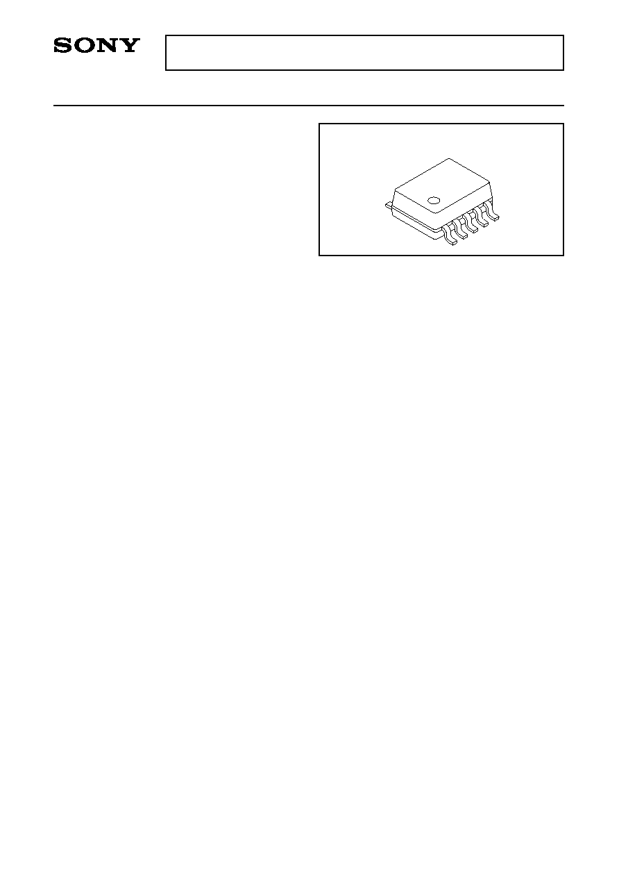
TSSOP-10pin
Application
SPDT switch for digital cellular telephones such as
JCDMA handsets.
Structure
GaAs J-FET MMIC
High Power SPDT Switch
10 pin (Plastic)
CXG1077TN
--2--
CXG1077TN
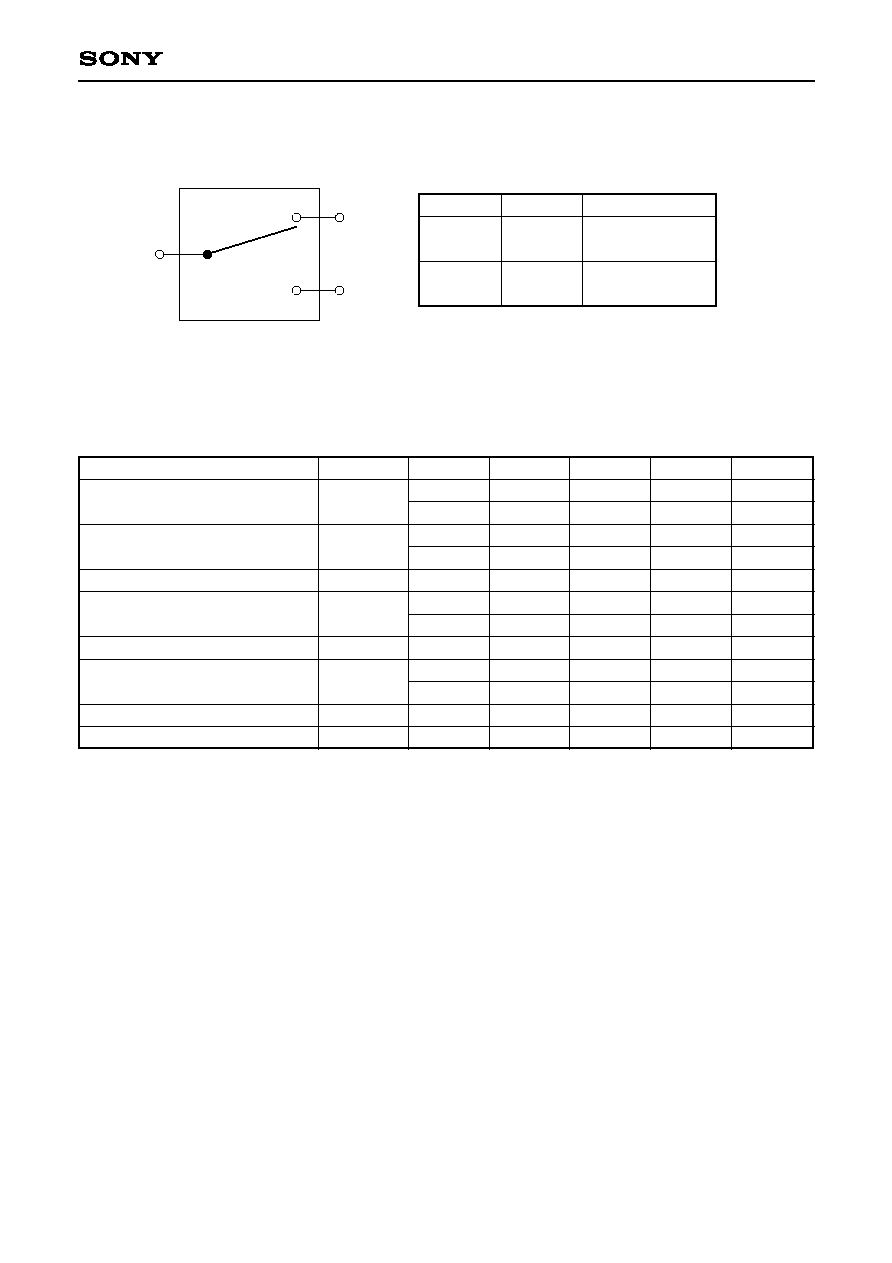
Block Diagram
RF3
RF1
RF2
VCTLA
High
Low
VCTLB
Low
High
RF1-RF2 ON
RF1-RF3 OFF
RF1-RF2 OFF
RF1-RF3 ON
Electrical Characteristics
(Ta=25 ∞C)
Insertion loss
Isolation
VSWR
Output harmonics
Input IP3
Input power for 1 dB compression
Switching speed TSW
Control current
Symbol
IL
ISO
VSWR
2fo, 3fo
IIP3
P1dB
TSW
I CTL
Min.
20
15
28
28
Typ.
0.35
0.5
22
17
1.2
60
33
33
100
30
Max.
0.6
0.8
1.4
≠30
≠30
54
300
50
Unit
dB
dB
dB
dB
dBm
dBm
dBm
dBm
dBm
ns
µA
1
Pin=25 dBm, 900 MHz, CW, 0/2.8 V Control
2
Pin=25 dBm, 1.8 GHz, CW, 0/2.8 V Control
3
Pin=21 dBm (900 MHz) +21 dBm (901 MHz), 0/2.8 V Control
Condition
1
2
1
2
1,
2
1
2
3
1
2

--3--
CXG1077TN
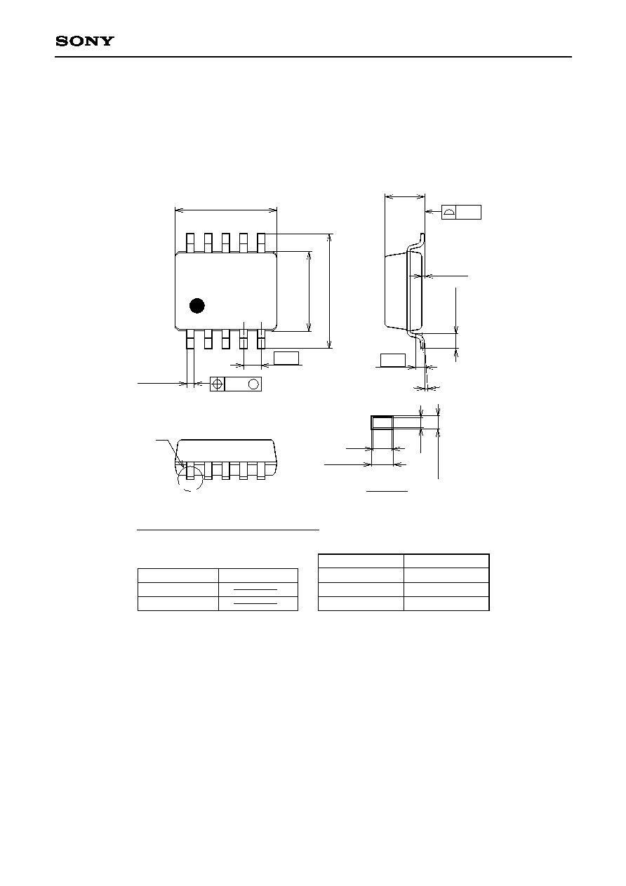
Package Outline/Pin Configuration
When using the CXG1077TN, the following external components should be used:
C1:
This is used for signal line filtering. 100 pF is recommended.
C2:
This is used for RF De-coupling and must be used in all applications. 100 pF is recommended.
Rctl: This resistor is used to give improved ESD performance.
10pin TSSOP (PLASTIC)
RF2
CTLA
GND
GND
GND
RF1
GND
GND
RF3
CTLB
10
1
Unit : mm
Recommended Circuit
CTLA
RF1
51k
CXG1077TN
C2 100pF
Rctl 1k
C1 100pF
RF2
C2 100pF
RF3
C2 100pF
6
7
8
9
10
CTLB
Rctl 1k
C1 100pF
1
2
3
4
5