
CXG1090EN
High Power 2
◊
4 Antenna Switch MMIC with Integrated Control Logic
Description
The CXG1090EN is a high power antenna switch
MMIC. This IC is suited to connect Tx/Rx to one of 4
antennas in cellular handset such as PDC.
The CXG1090EN has the integrated control logic
and can be operated with CMOS input.
This IC is designed using the Sony's GaAs J-FET
process which enable the CXG1090EN to be operated
with low voltage.
Features
∑ Low insertion loss: 0.30dB (Typ.)@900MHz, 0.40dB (Typ.)@1.5GHz
∑ Small package: 16-pin VSON
∑ High power handling: Pl dB: 37dBm
∑ CMOS compatible input control
∑ Low bias voltage: V
DD
= 3.0V
Applications
2
◊
4 antenna switch for digital cellular telephones such as PDC handsets
Structure
GaAs J-FET MMIC
Absolute Maximum Ratings
∑ Bias voltage
V
DD
7
V @Ta = 25∞C
∑ Control voltage
V
CTL
5
V @Ta = 25∞C
∑ Operating temperature Topr
≠35 to +85
∞C
∑ Storage temperature
Tstg
≠65 to +150
∞C
Note on Handling
GaAs MMICs are ESD sensitive devices. Special handling precautions are required.
≠ 1 ≠
E00222-PS
Sony reserves the right to change products and specifications without prior notice. This information does not convey any license by
any implication or otherwise under any patents or other right. Application circuits shown, if any, are typical examples illustrating the
operation of the devices. Sony cannot assume responsibility for any problems arising out of the use of these circuits.
16 pin VSON (Plastic)
≠ 2 ≠
CXG1090EN
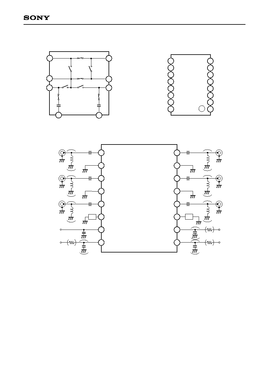
Block Diagram
RF5
(Rx)
RF4
(Ant/Ext.1)
RF6
(Diversity 1)
RF2
(Ant/Ext. 2)
RF3
(Tx)
RF1
(Diversity 2)
RF-GND6
RF-GND1
F1
F3
F6
F5
F7
F8
F2
F4
4
6
8
9
11
13
14
3
Pin Configuration
1
2
3
4
5
6
7
8
9
10
11
12
13
14
15
16
RF4
GND
RF5
GND
RF6
RF-GND6
V
DD
CTLA
RF3
GND
RF2
GND
RF1
RF-GND1
CTLC
CTLB
Recommended Circuit
1
2
3
4
5
6
7
8
9
10
11
12
13
14
15
16
RF3
GND
GND
RF-GND1
CTLC
CTLB
100pF
RF2
RF4
V
DD
CTLA
RF5
GND
GND
RF-GND6
RF6
100pF
100pF
100pF
L1
L1
L1
L1
100pF
100pF
100pF
100pF
1k
1k
RF1
L1
L1
Z6
Z1
100pF
1k
100pF
DC blocking capacitors (CRF) are needed.
Recommended to use bypass capacitors (Cbypass).
Recommended to use control resistors (RCTL), when it is necessary to improve the electrostatic discharge
strength (ESD).

≠ 4 ≠
CXG1090EN
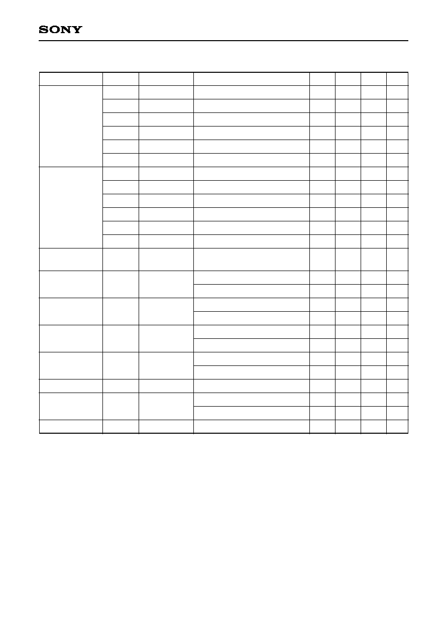
Electrical Characteristics 1
(V
CTL
(L) = 0V, V
CTL
(H) = 3V, Ta = 25∞C)
Item
Frequency
Condition
Pin = 29.5dBm, V
DD
= 2.8 to 3.0V
Pin = 29.5dBm, V
DD
= 2.8 to 3.0V
Pin = 7dBm, V
DD
= 2.8 to 3.0V
Pin = 7dBm, V
DD
= 2.8 to 3.0V
Pin = 7dBm, V
DD
= 2.8 to 3.0V
Pin = 7dBm, V
DD
= 2.8 to 3.0V
Pin = 29.5dBm, V
DD
= 2.8 to 3.0V
Pin = 29.5dBm, V
DD
= 2.8 to 3.0V
Pin = 7dBm, V
DD
= 2.8 to 3.0V
Pin = 7dBm, V
DD
= 2.8 to 3.0V
Pin = 7dBm, V
DD
= 2.8 to 3.0V
Pin = 7dBm, V
DD
= 2.8 to 3.0V
Pin = 29.5dBm, V
DD
= 3.0V
1
Pin = 29.5dBm, V
DD
= 2.8V
1
Pin = 29.5dBm, V
DD
= 3.0V
1
Pin = 29.5dBm, V
DD
= 2.8V
1
Pin = 29.5dBm, V
DD
= 3.0V
1
Pin = 29.5dBm, V
DD
= 2.8V
1
Pin = 29.5dBm, V
DD
= 3.0V
1
Pin = 29.5dBm, V
DD
= 2.8V
1
V
DD
= 3.0V
V
DD
= 2.8V
17
17
17
17
31
24
0.32
0.30
0.55
0.55
0.5
0.5
19
21
21
19
38
29
≠67
≠67
≠75
≠75
≠67
≠67
≠67
≠67
85
0.45
0.4
1.0
0.55
0.55
0.85
0.85
0.8
0.8
1.4
≠57
≠55
≠65
≠62
≠60
≠57
≠60
≠57
150
1
0.9
5.0
dB
dB
dB
dB
dB
dB
dB
dB
dB
dB
dB
dB
dBc
dBc
dBc
dBc
dBc
dBc
dBc
dBc
µA
mA
mA
µs
RF3-RF2
RF3-RF4
RF5-RF2
RF5-RF4
RF5-RF1
RF5-RF6
RF3-RF2
RF3-RF4
RF5-RF2
RF5-RF4
RF5-RF1
RF5-RF6
Each ON
Port
RF3-RF2
RF3-RF4
RF3-RF2
RF3-RF4
RF3-RF2
RF3-RF4
RF3-RF2
RF3-RF4
Insertion loss
Isolation
VSWR
ACP (±50kHz)
ACP (±100kHz)
2nd harmonics
3nd harmonics
Control current
Bias current
Switching speed
889 to 960MHz
889 to 960MHz
810 to 885MHz
810 to 885MHz
810 to 885MHz
810 to 885MHz
889 to 960MHz
889 to 960MHz
810 to 885MHz
810 to 885MHz
810 to 885MHz
810 to 885MHz
810 to 960MHz
889 to 960MHz
889 to 960MHz
889 to 960MHz
889 to 960MHz
Min.
Typ.
Max.
Unit
1
Input signal: ACP (±50kHz) < ≠65dBc, APC (±100kHz) < ≠75dBc,
2nd harmonics < ≠65dBc, 3rd harmonics < ≠65dBc
≠ 5 ≠
CXG1090EN
Electrical Characteristics 2
(V
CTL
(L) = 0V, V
CTL
(H) = 3V, Ta = 25∞C)
Item
Frequency
Condition
Pin = 29.5dBm, V
DD
= 2.8 to 3.0V
Pin = 29.5dBm, V
DD
= 2.8 to 3.0V
Pin = 7dBm, V
DD
= 2.8 to 3.0V
Pin = 7dBm, V
DD
= 2.8 to 3.0V
Pin = 7dBm, V
DD
= 2.8 to 3.0V
Pin = 7dBm, V
DD
= 2.8 to 3.0V
Pin = 29.5dBm, V
DD
= 2.8 to 3.0V
Pin = 29.5dBm, V
DD
= 2.8 to 3.0V
Pin = 7dBm, V
DD
= 2.8 to 3.0V
Pin = 7dBm, V
DD
= 2.8 to 3.0V
Pin = 7dBm, V
DD
= 2.8 to 3.0V
Pin = 7dBm, V
DD
= 2.8 to 3.0V
Pin = 29.5dBm, V
DD
= 3.0V
1
Pin = 29.5dBm, V
DD
= 2.8V
1
Pin = 29.5dBm, V
DD
= 3.0V
1
Pin = 29.5dBm, V
DD
= 2.8V
1
Pin = 29.5dBm, V
DD
= 3.0V
1
Pin = 29.5dBm, V
DD
= 2.8V
1
Pin = 29.5dBm, V
DD
= 3.0V
1
Pin = 29.5dBm, V
DD
= 2.8V
1
V
DD
= 3.0V
V
DD
= 2.8V
12
15
15
13
35
20
0.40
0.40
0.65
0.65
0.60
0.60
15
18
18
16
40
25
≠67
≠67
≠75
≠75
≠67
≠67
≠67
≠67
85
0.45
0.4
1.0
0.70
0.70
0.95
0.95
0.90
0.90
1.4
≠55
≠53
≠65
≠62
≠60
≠57
≠57
≠55
150
1
0.9
5.0
dB
dB
dB
dB
dB
dB
dB
dB
dB
dB
dB
dB
dBc
dBc
dBc
dBc
dBc
dBc
dBc
dBc
µA
mA
mA
µs
RF3-RF2
RF3-RF4
RF5-RF2
RF5-RF4
RF5-RF1
RF5-RF6
RF3-RF2
RF3-RF4
RF5-RF2
RF5-RF4
RF5-RF1
RF5-RF6
Each ON
Port
RF3-RF2
RF3-RF4
RF3-RF2
RF3-RF4
RF3-RF2
RF3-RF4
RF3-RF2
RF3-RF4
Insertion loss
Isolation
VSWR
ACP (±50kHz)
ACP (±100kHz)
2nd harmonics
3nd harmonics
Control current
Bias current
Switching speed
1429 to 1453MHz
1429 to 1453MHz
1477 to 1501MHz
1477 to 1501MHz
1477 to 1501MHz
1477 to 1501MHz
1429 to 1453MHz
1429 to 1453MHz
1477 to 1501MHz
1477 to 1501MHz
1477 to 1501MHz
1477 to 1501MHz
1429 to 1501MHz
1429 to 1453MHz
1429 to 1453MHz
1429 to 1453MHz
1429 to 1453MHz
Min.
Typ.
Max.
Unit
1
Input signal: ACP (±50kHz) < ≠65dBc, APC (±100kHz) < ≠75dBc,
2nd harmonics < ≠65dBc, 3rd harmonics < ≠65dBc

≠ 6 ≠
CXG1090EN
Package Outline
Unit: mm
0.05
SONY CODE
EIAJ CODE
JEDEC CODE
PACKAGE MATERIAL
LEAD TREATMENT
LEAD MATERIAL
PACKAGE MASS
EPOXY RESIN
SOLDER PLATING
COPPER ALLOY
PACKAGE STRUCTURE
TERMINAL SECTION
0
.
2
±
0
.
0
1
0
.
2
3
±
0
.
0
2
0
.
0
3
±
0
.
0
3
Soldrer Plating
0.14
ranges of 0.1mm and 0.25mm from the end of a terminal.
NOTE: 1) The dimensions of the terminal section apply to the
16PIN VSON(PLASTIC)
VSON-16P-01
0.02 g
0.2 S B
A
3.5
2
.
7
2
.
5
0.4
B
0.2 S
B
A
0.05 M S A-B
2x
4x
S
S
0.9 MAX
0.6
0
.
5
±
0
.
2
0.13 ± 0.025
+ 0.09
≠ 0.03
1.4
0.35 ± 0.1
0
.
3
5
±
0
.
1
