 | –≠–ª–µ–∫—Ç—Ä–æ–Ω–Ω—ã–π –∫–æ–º–ø–æ–Ω–µ–Ω—Ç: CXG1194XR | –°–∫–∞—á–∞—Ç—å:  PDF PDF  ZIP ZIP |
- 1 -
E05X02-PS
This IC is ESD sensitive device. Special handling precautions are required.
The actual ESD test data will be available later.
Sony reserves the right to change products and specifications without prior notice. This information does not convey any license
by any implication or otherwise under any patents or other right. Application circuits shown, if any, are typical examples illustrating
the operation of the devices. Sony cannot assume responsibility for any problems arising out of the use of these circuits.
CXG1194XR
SP4T Antenna Switch for GSM/UMTS
Description
The CXG1194XR is a high power SP4T antenna switch for GSM/UMTS applications. The low insertion loss on
transmit means increased talk time as the Tx power amplifier can be operated at a lower output level. On chip
logic reduces component count and simplifies the PCB layout by allowing direct connection of the switch to
digital baseband control lines with CMOS logic levels. This switch is SP4T, one antenna can be routed to either
of the 2Tx or 2Rx ports. It requires 2 CMOS control lines. The Sony GaAs JPHEMT MMIC process is used for
low insertion loss.
(Applications: GSM dual-band handsets, GSM/UMTS dual-mode handsets)
Features
Insertion loss (Tx) : 0.35dB (Typ.) at 34dBm (GSM900)
0.45dB (Typ.) at 32dBm (GSM1800)
Package
Small and Low height package size: 14-pin XQFN (2.5mm
◊
2.5mm
◊
0.35mm (Typ.))
Structure
GaAs JPHEMT MMIC
CXG1194XR
- 2 -
Absolute Maximum Ratings
(Ta = 25
∞
C)
Copper-clad lamination of glass board (4 layers) : 30mm square, t = 0.8mm, FR-4.
Note) Use this product without exceeding the PD value specified in this specification.
If it is used with exceeding the PD value even for a moment, the heat generated by the operation may
cause the degradation or breakdown of the product.
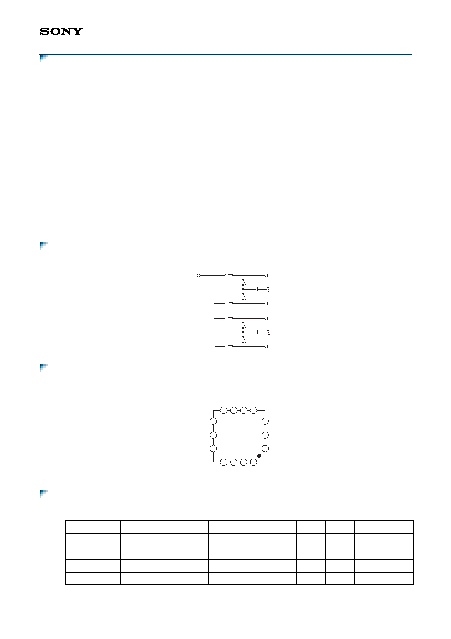
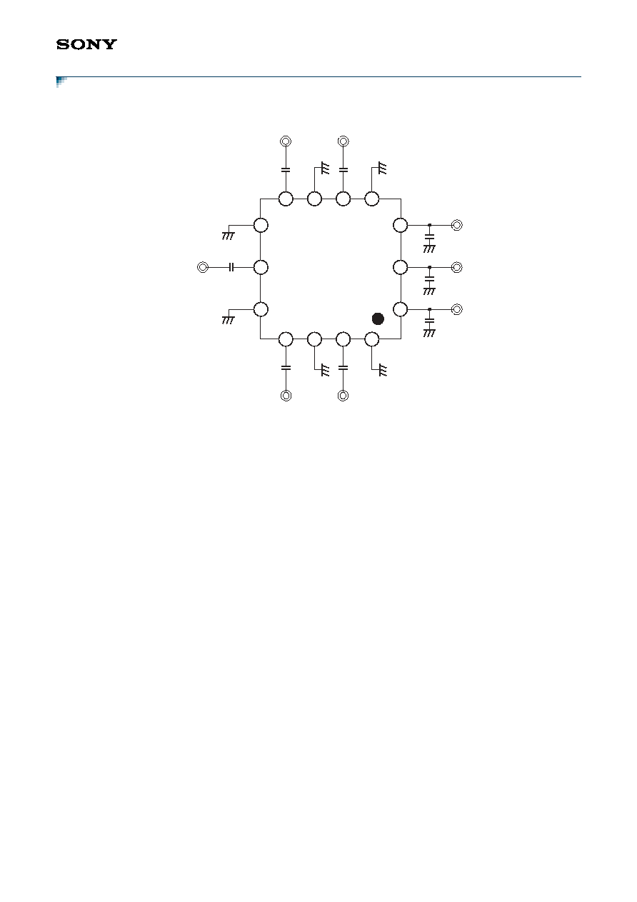
Block Diagram
Pin Configuration
Truth Table
Bias Voltage
V
DD
7
V
Control Voltage
Vctl
5
V
Input power max. [ANT, RF1, RF4]
35
dBm (Duty cycle = 12.5 to 50%)
Input power max. [RF2, RF3]
13
dBm
Operating temperature
Topr
≠35 to +85
∞
C
Maximum power dissipation
PD
500
mW
ANT
RF1 (Tx)
RF4 (Tx)
F4
RF3 (Rx)
F3
F7
F8
RF2 (Rx)
F2
F1
F5
F6
11
12
13
14
7
6
5
4
3
2
1
RF1
GND
ANT
GND
RF3
GND
RF4
GND
V
DD
CTLA
CTLB
8
9
10
GND
RF2
GND
ON Path
CTLA
CTLB
F1
F2
F3
F4
F5
F6
F7
F8
ANT ≠ RF1
L
L
ON
OFF
OFF
OFF
OFF
ON
ON
ON
ANT ≠ RF2
H
L
OFF
ON
OFF
OFF
ON
OFF
ON
ON
ANT ≠ RF3
L
H
OFF
OFF
ON
OFF
ON
ON
OFF
ON
ANT ≠ RF4
H
H
OFF
OFF
OFF
ON
ON
ON
ON
OFF
CXG1194XR
- 3 -
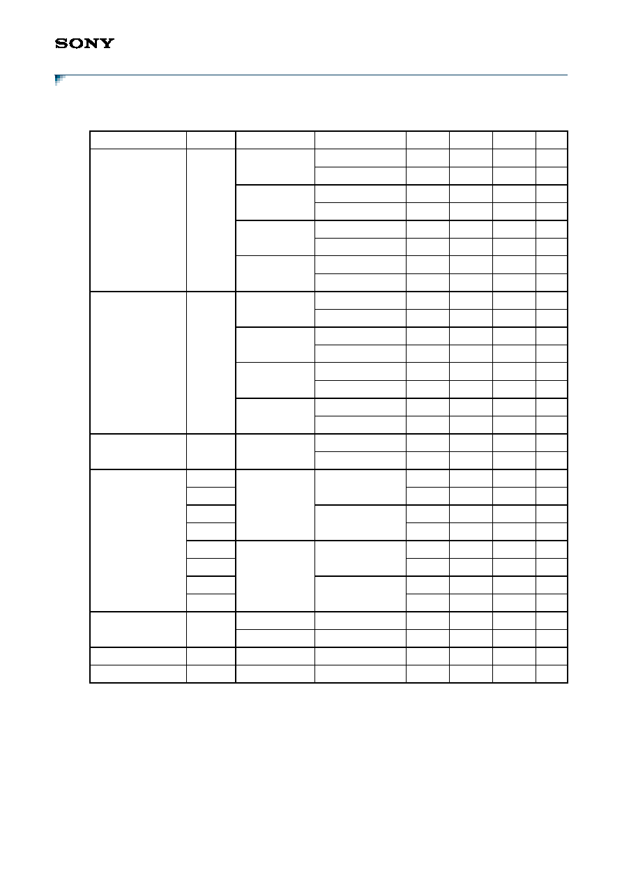
Electrical Characteristics
(Ta = 25
∞
C)
Note) Electrical Characteristics are measured with all RF ports terminated in 50
.
*1
Harmonics measured with Tx inputs harmonically matched. The use of harmonic matching is recommended
to ensure optimum performance.
*2
Power incident on Tx, Pin = 34dBm, 824 to 915MHz, V
DD
= 2.8V, RF1 or RF4 enabled
*3
Power incident on Tx, Pin = 32dBm, 1710 to 1910MHz, V
DD
= 2.8V, RF1 or RF4 enabled
Item
Symbol
Port
Condition
Min.
Typ.
Max.
Unit
Insertion loss
IL
ANT ≠ RF1
824 to 960MHz
0.35
0.50
dB
1710 to 1990MHz
0.45
0.65
dB
ANT ≠ RF2
824 to 960MHz
0.45
0.60
dB
1710 to 1990MHz
0.55
0.70
dB
ANT ≠ RF3
824 to 960MHz
0.45
0.60
dB
1710 to 1990MHz
0.55
0.70
dB
ANT ≠ RF4
824 to 960MHz
0.35
0.50
dB
1710 to 1990MHz
0.45
0.65
dB
Isolation
ISO.
ANT ≠ RF1
824 to 960MHz
25
30
dB
1710 to 1990MHz
22
26
dB
ANT ≠ RF2
824 to 960MHz
30
35
dB
1710 to 1990MHz
25
30
dB
ANT ≠ RF3
824 to 960MHz
30
35
dB
1710 to 1990MHz
25
30
dB
ANT ≠ RF4
824 to 960MHz
30
35
dB
1710 to 1990MHz
25
30
dB
VSWR
VSWR
824 to 960MHz
1.2
--
1710 to 1990MHz
1.2
--
Harmonics
*1
2fo
ANT ≠ RF1
*2
≠33
≠28
dBm
3fo
≠34
≠28
dBm
2fo
*3
≠35
≠30
dBm
3fo
≠37
≠33
dBm
2fo
ANT ≠ RF4
*2
≠34
≠30
dBm
3fo
≠35
≠30
dBm
2fo
*3
≠35
≠30
dBm
3fo
≠38
≠34
dBm
P
1dB
compression
input power
P
1dB
ANT ≠ RF1, 4
*2
35
dBm
ANT ≠ RF1, 4
*3
33
dBm
Control current
Ictl
Vctl = 2.8V
15
40
µ
A
Supply current
I
DD
V
DD
= 2.8V
0.12
0.23
mA
CXG1194XR
- 4 -
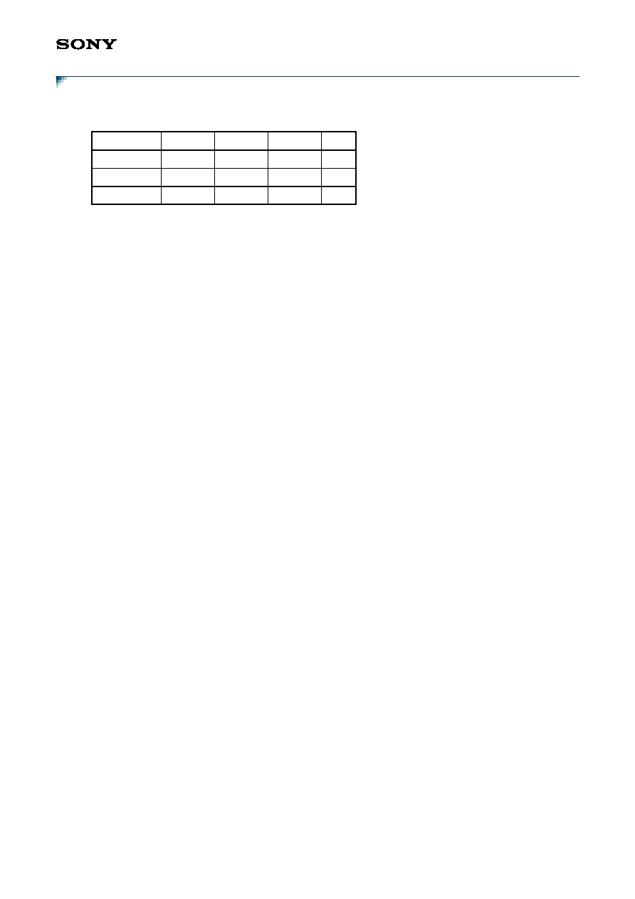
DC Bias Condition
(Ta = 25
∞
C)
Item
Min.
Typ.
Max.
Unit
Vctl (H)
2.0
2.8
3.6
V
Vctl (L)
0
--
0.4
V
V
DD
2.6
2.8
3.6
V
CXG1194XR
- 5 -
Recommended Circuit
11
12
13
14
7
6
5
4
3
2
1
RF1
ANT
GND
GND
RF3
V
DD
Cbypass
CTLA
Cbypass
CTLB
Cbypass
8
9
10
RF2
C
RF
C
RF
C
RF
C
RF
RF4
C
RF
GND
GND
GND
GND
When using this IC, the following external components should be used:
C
RF
: This capacitor is used for RF decoupling and must be used for all applications.
Cbypass: This capacitor is used for DC line filtering. 100pF is recommended.
CXG1194XR
- 6 -
Sony Corporation
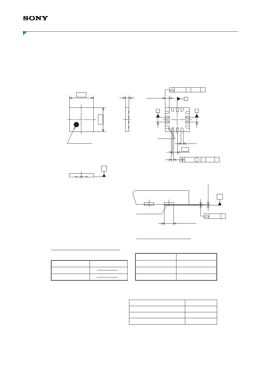
Package Outline
(Unit: mm)
SONY CODE
EIAJ CODE
JEDEC CODE
XQFN-14P-01
14PIN XQFN (PLASTIC)
TERMINAL SECTION
Note:Cutting burr of lead are 0.05mm MAX.
PACKAGE MATERIAL
LEAD TREATMENT
LEAD MATERIAL
EPOXY RESIN
SOLDER PLATING
COPPER ALLOY
PACKAGE STRUCTURE
PACKAGE MASS
C
S
S
3
A
B
C
S A-B
M
S
PIN 1 INDEX
10
11
14
1
4
7
8
0.35 ± 0.05
0.4 ± 0.1
8-C0.1
0.24
0.5
0.05
0.05
0.24
+0.09
-0.03
MAX 0.02
Solder Plating
0.01g
2.5
2.5
C
A-B
S
x4
0.05
LEAD PLATING SPECIFICATIONS
ITEM
LEAD MATERIAL
COPPER ALLOY
SOLDER COMPOSITION
Sn-Bi Bi:1-4wt%
PLATING THICKNESS
5-18µm
SPEC.