- 1 -
E05X06-PS
GaAs MMICs are ESD sensitive devices.Special handing precautions are required.
Sony reserves the right to change products and specifications without prior notice. This information does not convey any license
by any implication or otherwise under any patents or other right. Application circuits shown, if any, are typical examples illustrating
the operation of the devices. Sony cannot assume responsibility for any problems arising out of the use of these circuits.
CXG1213XR
High Power DPDT Switch with Logic Control
Description
This CXG1213XR can be used in wireless communication systems, for example, W-CDMA handsets.
The IC has on-chip logic for operation with 2 CMOS control inputs.
The Sony JPHEMT process is used for low insertion loss and on-chip logic circuit.
(Applications: Antenna switch for cellular handsets, dual-band W-CDMA)
Features
Low insertion loss
2 CMOS compatible control line
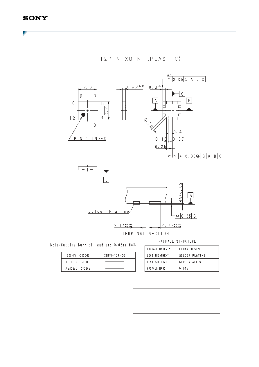
Package
Small package size: 12-pin XQFN
Structure
GaAs JPHEMT MMIC
Absolute Maximum Ratings
(Ta = 25
°
C)
Bias voltage
V
DD
7
V
Control voltage
Vctl
5
V
Operating temperature Topr
35 to +85
°
C
Storage temperature
Tstg
65 to +150
°
C
CXG1213XR
- 2 -
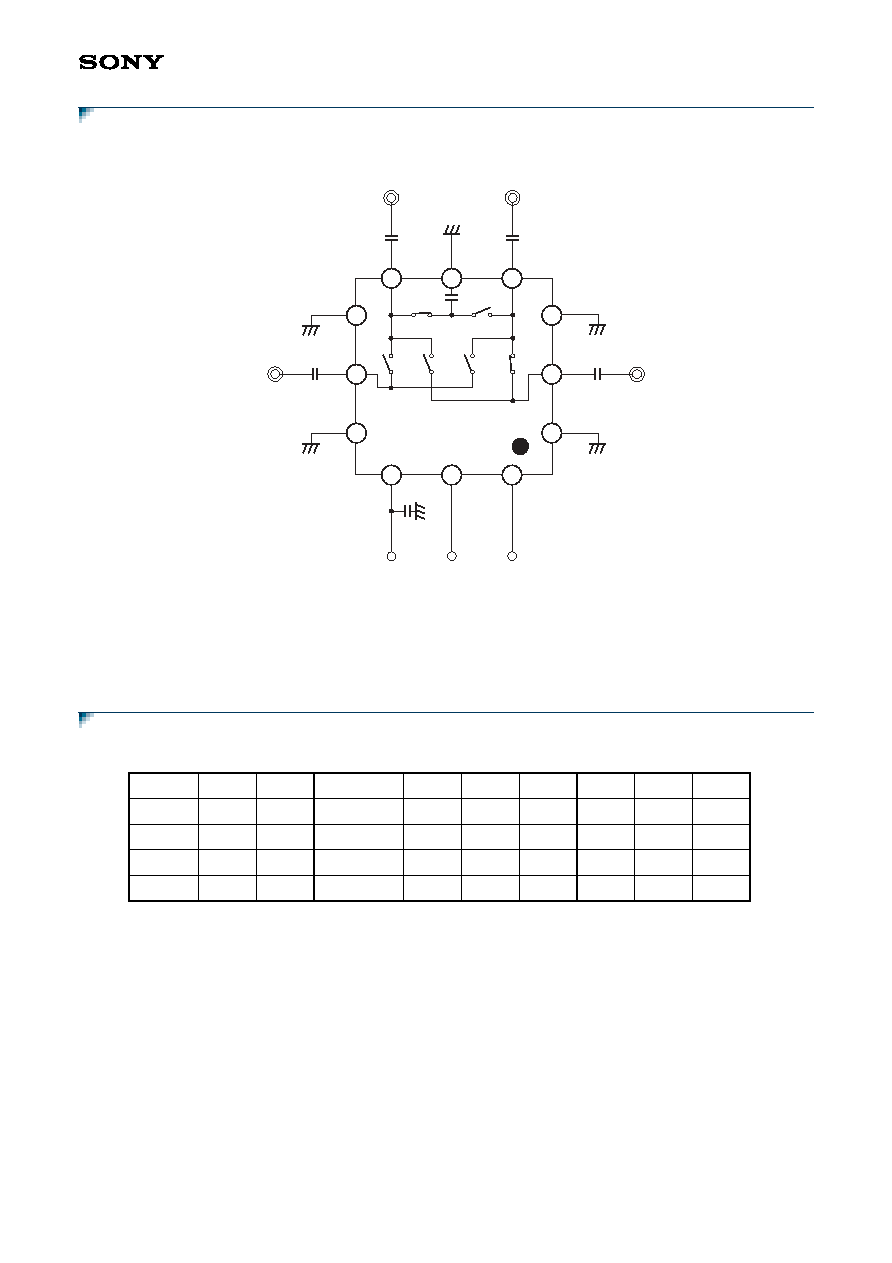
Block Diagram and Recommended Circuit
Truth Table
Cbypass
(100pF)
V
DD
CTLA
CTLB
RF4
10
11
12
6
5
4
3
2
1
GND
GND
RF2
7
8
9
RF1
C
RF
(27pF)
C
RF
(27pF)
RF3
GND
GND
GND
When using this IC, the following external components should be used:
C
RF
: This capacitor is used for RF decoupling and must be used for all applications.
Cbypass: This capacitor is used for DC line filtering. 100pF is recommended.
C
RF
(1000pF)
C
RF
(1000pF)
F3
F4
F6
F2
F5
F1
State
CTLA
CTLB
ON Path
F1
F2
F3
F4
F5
F6
1
L
L
RF4 RF3
OFF
OFF
ON
OFF
OFF
ON
2
L
H
RF4 RF2
OFF
OFF
OFF
ON
ON
OFF
3
H
L
RF1 RF3
OFF
ON
ON
OFF
OFF
OFF
4
H
H
RF1 RF2
ON
OFF
OFF
ON
OFF
OFF
CXG1213XR
- 3 -
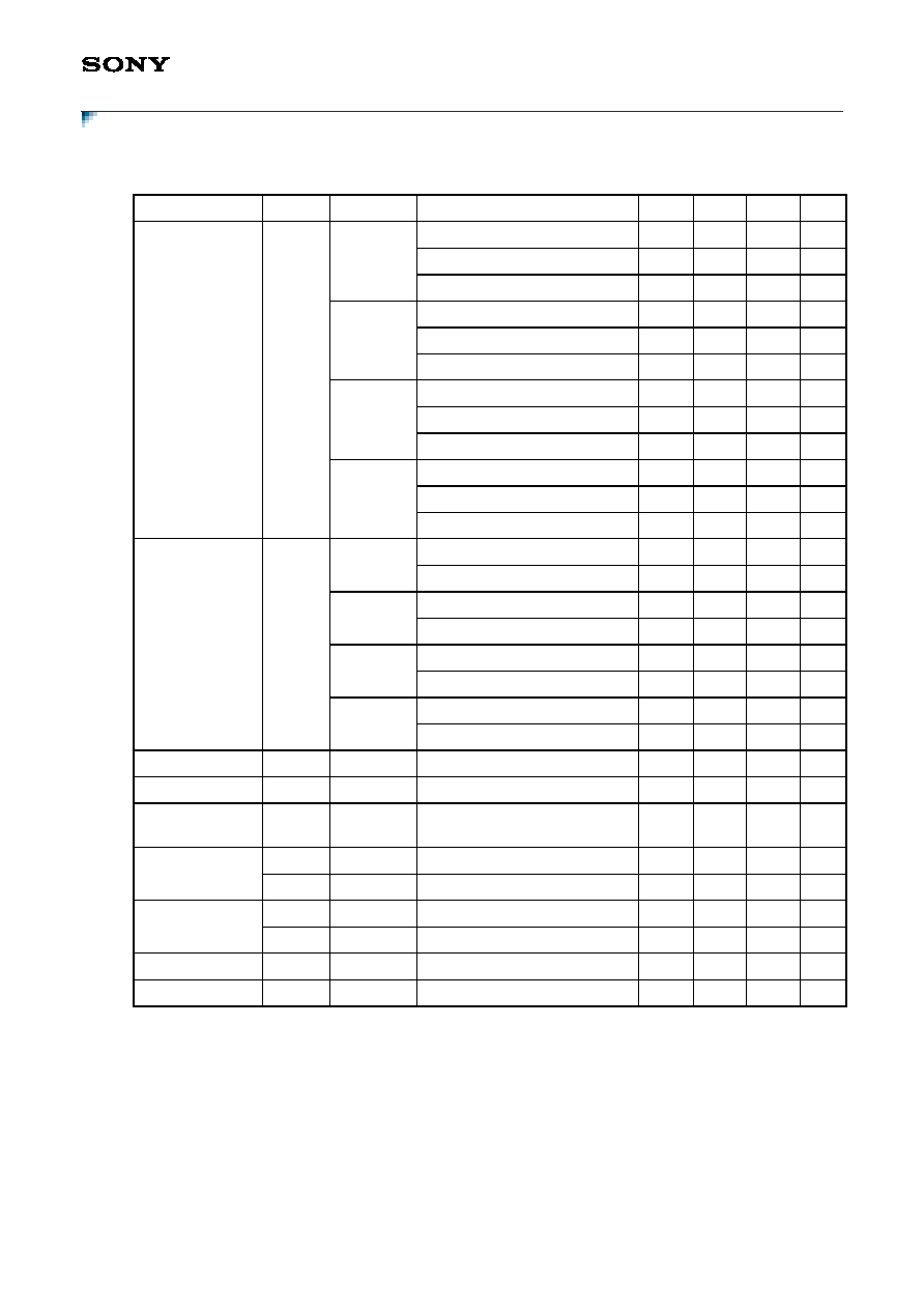
Electrical Characteristics
(Ta = 25
°
C)
*1
Pin = 25dBm, 0/1.85V control, V
DD
= 2.85V, 830 to 840MHz, 1920 to 1980MHz
Item
Symbol
State
Condition
Min.
Typ.
Max.
Unit
Insertion loss
IL
1
RF4 RF3, 830 to 885MHz
0.25
0.45
dB
1920 to 1980MHz
0.40
0.65
dB
2110 to 2170MHz
0.45
0.70
dB
2
RF4 RF2, 830 to 885MHz
0.25
0.45
dB
1920 to 1980MHz
0.40
0.65
dB
2110 to 2170MHz
0.45
0.70
dB
3
RF1 RF3, 830 to 885MHz
0.25
0.45
dB
1920 to 1980MHz
0.40
0.65
dB
2110 to 2170MHz
0.45
0.70
dB
4
RF1 RF2, 830 to 885MHz
0.25
0.45
dB
1920 to 1980MHz
0.40
0.65
dB
2110 to 2170MHz
0.45
0.70
dB
Isolation
ISO.
2
RF4 RF3, 830 to 885MHz
20
25
dB
1920 to 2170MHz
15
20
dB
1
RF4 RF2, 830 to 885MHz
25
30
dB
1920 to 2170MHz
20
25
dB
4
RF1 RF3, 830 to 885MHz
25
30
dB
1920 to 2170MHz
18
23
dB
3
RF1 RF2, 830 to 885MHz
20
25
dB
1920 to 2170MHz
15
20
dB
VSWR
VSWR
50
1.2
--
Switching speed
TSW
5
10
µ
s
1dB compression
input power
P1dB
V
DD
= 2.85V
32
dBm
ACLR
ACLR1
±
5MHz, 3.84MHz BW
*1
60
50
dBc
ACLR2
±
10MHz, 3.84MHz BW
*1
65
55
dBc
Harmonics
2fo
*1
70
dBc
3fo
*1
70
dBc
Bias current
I
DD
V
DD
= 2.85V
80
150
µ
A
Control current
Ictl
Vctl (H) = 1.85V
10
20
µ
A