 | –≠–ª–µ–∫—Ç—Ä–æ–Ω–Ω—ã–π –∫–æ–º–ø–æ–Ω–µ–Ω—Ç: CXG7001FN | –°–∫–∞—á–∞—Ç—å:  PDF PDF  ZIP ZIP |

≠ 1 ≠
E04139-PS
Sony reserves the right to change products and specifications without prior notice. This information does not convey any license by
any implication or otherwise under any patents or other right. Application circuits shown, if any, are typical examples illustrating the
operation of the devices. Sony cannot assume responsibility for any problems arising out of the use of these circuits.
CXG7001FN
26 pin HSOF (Plastic)
Power Amplifier/Antenna Switch + Low Noise Down Conversion Mixer for PHS
Notes on Handling
GaAs MMICs are ESD sensitive devices. Special handling precautions are required.
Description
The CXG7001FN is a MMIC consisting of the
power amplifier, antenna switch and low noise down
conversion mixer.
This IC is designed using the Sony's GaAs J-FET
process featuring a single positive power supply
operation.
Features
∑ Operates at a single positive power supply: V
DD
= 3V
∑ Small mold package: 26-pin HSOF
<Power amplifier/antenna switch transmitter block >
∑ Low current consumption: I
DD
= 150mA
(P
OUT
= 20.2dBm, f = 1.9GHz)
∑ High power gain: Gp = 39dB Typ.
(P
OUT
= 20.2dBm, f = 1.9GHz)
<Antenna switch receiver block/
low noise down conversion mixer>
∑ Low current consumption: I
DD
= 5.5mA Typ.
(When no signal)
∑ High conversion gain: Gc = 20.5dB Typ. (f = 1.9GHz)
∑ Low distortion: Input IP3 = ≠13dBm Typ. (f = 1.9GHz)
∑ High image suppression ratio: IMR = 40dBc Typ.
(f = 1.9GHz)
∑ High 1/2 IF suppression ratio: 1/2IFR = 44dBc Typ.
(f = 1.9GHz)
Applications
Japan digital cordless telephones (PHS)
Structure
GaAs J-FET MMIC
Absolute Maximum Ratings
<Power amplifier block>
∑ Supply voltage
V
DD
6
V
∑ Voltage between gate and source
V
GSO
1.5
V
∑ Gain control voltage
VP
CTL
2.5
V
∑ Drain current
I
DD
550
mA
∑ Allowable power dissipation
P
D
3
W
<Switch block>
Control voltage
V
CTL
6
V
<Front-end block>
∑ Supply voltage
V
DD
6
V
∑ Input power
P
RF
+10
dBm
<Common to each block>
∑ Channel temperature
Tch
150
∞C
∑ Operating temperature
Topr
≠35 to +85
∞C
∑ Storage temperature
Tstg
≠65 to +150
∞C
Recommended Operating Conditions
<Common to each block>
∑ Supply voltage
V
DD
2.7 to 3.3
V
<Power amplifier block>
∑ Gain control voltage
VP
CTL
to V
DD
≠1.0
V
<Switch block>
∑ Control voltage (H)
V
CTL
(H) 2.9 to 3.3
V
∑ Control voltage (L)
V
CTL
(L)
0 to 0.2
V
≠ 2 ≠
CXG7001FN
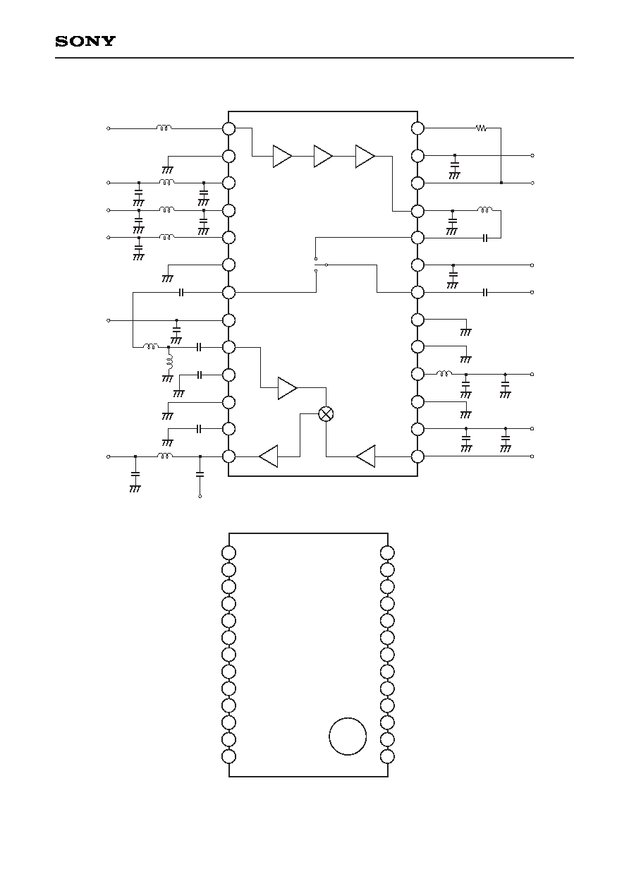
Block Diagram and External Circuit
Pin Configuration
30pF
2.2nH
P
IN
18nH
1nF
1nF
V
DD
1
18nH
1nF
30pF
V
DD
2
82nH
1nF
5pF
100pF
1.8nH
10nF
V
DD
3
V
CTL
2
V
DD
(IF AMP, MIX)
(P
OUT
)
(T
X
)
1pF
100pF
IF
OUT
30pF
100nF
13pF
10pF
10nH
6.8nH
(RF
IN
)
(R
X
)
V
DD
(LO AMP)
LO
IN
V
CTL
1
30pF
2.2nH
3.9nH
V
DD
(RF AMP)
1nF
18pF
1nF
13pF
1
2
3
4
5
6
7
8
9
10
11
12
13
14
15
16
17
18
19
21
20
22
23
24
25
26
ANT
100pF
1k
(V
GG
1)
VP
CTL
V
GG
2
V
GG
1
VP
CTL
V
GG
2
P
OUT
Tx
V
CTL
1
ANT
GND
GND
V
DD
(RF AMP)
GND
V
DD
(LO AMP)
LO
IN
P
IN
GND
V
DD
1
V
DD
2
V
DD
3
GND
R
X
V
CTL
2
RF
IN
CAP
GND
CAP
IF
OUT
/V
DD
(IF AMP, MIX)
1
2
3
4
5
6
7
8
9
10
11
12
13
14
15
16
17
18
19
21
20
22
23
24
25
26
26 pin ≠ HSOF (Plastic)
≠ 3 ≠
CXG7001FN
Pin Description
Pin No.
1
2
3
4
5
6
7
8
9
10
11
12
13
14
15
16
17
18
19
20
21
22
23
24
25
26
Symbol
LO
IN
V
DD
(LO AMP)
GND
V
DD
(RF AMP)
GND
GND
ANT
V
CTL
1
T
X
P
OUT
V
GG
2
VP
CTL
V
GG
1
P
IN
GND
V
DD
1
V
DD
2
V
DD
3
GND
R
X
V
CTL
2
RF
IN
CAP
GND
CAP
IF
OUT
/V
DD
(IF AMP, MIX)
Description
LO signal input.
LO AMP V
DD
.
GND.
RF AMP V
DD
.
GND.
GND.
Antenna switch.
Either ANT-Tx or ANT-Rx is depending on whether the setting is VCTL1 or
VCTL 2.
Antenna switch control Pin 1.
Tx.
Input the signal into the antenna switch when ANT-Tx.
Power amplifier output.
Power amplifier (the final-stage FET) gate voltage adjustment Pin 2.
The first-stage FET control pin for the power amplifier.
Power amplifier (the first-stage FET, the second-stage FET) gate voltage
adjustment Pin 1.
Signal input into the power amplifier.
GND.
Power amplifier (the first-stage FET) V
DD
1.
Power amplifier (the second-stage FET) V
DD
2.
Power amplifier (the final-stage FET) V
DD
3.
GND.
Rx.
Output ANT input signal into Rx when ANT-Rx.
Antenna switch control Pin 2.
RF signal input.
Connector for the external capacitor.
Connected to LNA FET source. Self-vibration frequency becomes 1.9GHz by
this capacitor (Typ. 13pF).
GND.
Connector for the external capacitor.
IF AMP distortion is corrected by this capacitor.
IF output and IF AMP, MIX V
DD
.
≠ 4 ≠
CXG7001FN
Electrical Characteristics
1. Control Pin Logic for Antenna Switch
Conditions of control pins
V
CTL
1 = 3V, V
CTL
2 = 0V
V
CTL
1 = 0V, V
CTL
2 = 3V
ANT ≠ T
X
ON
OFF
ANT ≠ R
X
OFF
ON
2. Power Amplifier Block + Antenna Switch Transmitter Block
These specifications are those when the Sony's recommended evaluation board, shown on page 7, is used.
Unless otherwise specified: V
DD
= 3V, VP
CTL
= 2V, V
CTL
1 = 3V, V
CTL
2 = 0V,
I
DD
= 150mA, P
OUT
= 20.2dBm, f = 1.9GHz, Ta = 25∞C
Unit
Item
Current consumption
Gate voltage adjustment value
Output power
Power gain
Adjacent channel leak power ratio
(600 ± 100kHz)
Adjacent channel leak power ratio
(900 ± 100kHz)
Occupied bandwidth
2nd-order harmonic level
3rd-order harmonic level
Measured with the ANT pin
Measured with the ANT pin
Measured with the ANT pin
Measured with the ANT pin
Measured with the ANT pin
Measured with the ANT pin
Measurement conditions
mA
V
dBm
dB
dBc
dBc
kHz
dBc
dBc
Symbol
I
DD
V
GG
P
OUT
G
P
ACPR600kHz
ACPR900kHz
OBW
--
--
3. Antenna Switch Receiver Block + Low Noise Down Conversion Mixer Block
These specifications are those when the Sony's recommended evaluation board, shown on page 7, is used.
Unless otherwise specified: V
DD
= 3V, V
CTL
1 = 0V, V
CTL
2 = 3V, RF1 = 1.90GHz/≠35dBm,
LO = 1.66GHz/≠15dBm, Ta = 25∞C
Unit
Max.
7.5
5.5
≠37
Typ.
5.5
20.5
4.2
≠13
40
44
47
62
≠42
Min.
17
≠17.5
30
39
39
24
Item
Current consumption
Conversion gain
Noise figure
Input IP3
Image suppression ratio
1/2 IF suppression ratio
2
◊
LO≠IF suppression ratio
2
◊
LO+IF suppression ratio
LO to ANT leak
When no signal
When a small signal
When a small signal
1
RF2 = 1.42GHz/≠35dBm
RF2 = 1.78GHz/≠35dBm
RF2 = 3.08GHz/≠35dBm
RF2 = 3.56GHz/≠35dBm
Measurement conditions
mA
dB
dB
dBm
dBc
dBc
dBc
dBc
dBm
Symbol
I
DD
G
C
NF
IIP3
IMR
1/2IFR
--
--
P
LK
1
Conversion from IM3 suppression ratio during FR1 = 1.9000GHz/≠35dBm and FR2 = 1.9006GHz/≠35dBm input.
Max.
0.60
≠55
≠60
275
≠25
≠25
Typ.
150
0.25
39
≠63
≠70
250
Min.
0.04
20.2
36

≠ 5 ≠
CXG7001FN
Example of Representative Characteristics
1. Power Amplifier + Antenna Switch Transmitter Block (f = 1.9GHz, Ta = 25∞C)
P
OUT
, ACPR600kHz vs. P
IN
P
IN
≠ Input power [dBm]
P
OUT
≠ Output po
w
er [dBm]
A
C
PR600kHz ≠ Adjacent channel leak po
w
er r
atio [dBc]
≠40
≠35
≠30
≠25
≠20
≠15
≠10
≠70
≠65
≠60
≠55
≠50
≠45
≠40
≠5
0
5
10
15
20
25
V
DD
≠ Supply voltage [V]
P
OUT
≠ Output po
w
er [dBm]
A
C
PR600kHz ≠ Adjacent channel leak po
w
er r
atio [dBc]
2.0
2.5
3.0
3.5
4.0
4.5
5.0
≠70
≠65
≠60
≠55
≠50
≠45
≠40
17
18
19
20
21
22
P
OUT
23
ACPR600kHz
ACPR600kHz
V
DD
= 3V, VP
CTL
= 2V, V
GG
= const., V
CTL
1 = 3V,
V
CTL
2 = 0V
I
DD
= 150mA (@P
OUT
= 20.2dBm), P
IN
= var.
V
DD
= 3V, VP
CTL
= var., V
GG
= const., V
CTL
1 = 3V,
V
CTL
2 = 0V
I
DD
= 150mA (@VP
CTL
= 2V), P
IN
= var.,
P
OUT
= 20.2dBm
Gp, ACPR600kHz vs. VP
CTL
VP
CTL
≠ Gain control voltage [V]
G
p
≠ P
o
w
e
r gain [dB]
A
C
PR600kHz ≠ Adjacent channel leak po
w
er r
atio [dBc]
0
0.5
1.0
1.5
2.0
2.5
3.0
≠70
≠65
≠60
≠55
≠50
≠45
≠40
15
20
25
30
35
40
45
G
P
ACPR600kHz
P
OUT
V
DD
= 3V, VP
CTL
= 2V, V
GG
= var., V
CTL
1 = 3V,
V
CTL
2 = 0V
I
DD
= var., P
IN
= var., P
OUT
= 20.2dBm
Gp, ACPR600kHz vs. I
DD
V
DD
= var., VP
CTL
= 2V, V
GG
= const., V
CTL
1 = 3V,
V
CTL
2 = 0V
I
DD
= 150mA (@V
DD
= 3V, P
OUT
= 20.2dBm),
P
IN
= ≠19.3dBm
P
OUT
, ACPR600kHz vs. V
DD
I
DD
≠ Current consumption [mA]
G
p
≠ P
o
w
e
r gain [dB]
A
C
PR600kHz ≠ Adjacent channel leak po
w
er r
atio [dBc]
100
120
140
160
180
200
220
≠70
≠65
≠60
≠55
≠50
≠45
≠40
36
37
38
39
40
41
42
G
P
ACPR600kHz

≠ 6 ≠
CXG7001FN
2. Antenna Switch Receiver Block + Low Noise Down Conversion Mixer (Ta = 25∞C)
G
C
, NF vs. P
LO
P
LO
≠ Local input [dBm]
G
C
≠ Con
v
e
r
tion gain [dB]
≠25
≠20
≠15
≠10
≠5
0
16
17
18
19
20
21
22
4.00
4.25
4.50
4.75
5.00
5.25
5.50
V
DD
= 3V, V
CTL
1 = 0V, V
CTL
2 = 3V,
RF = 1.90GHz/small signal, LO = 1.66GHz
V
DD
= 3V, V
CTL
1 = 0V, V
CTL
2 = 3V,
RF = 1.90GHz/≠35dBm, LO = 1.66GHz
V
DD
= 3V, V
CTL
1 = 0V, V
CTL
2 = 3V,
RF1 = 1.9000GHz, RF2 = 1.9006GHz,
LO = 1.66GHz/≠15dBm
P
OUT
, P
IM3
vs. P
IN
P
IN
≠ RF input power [dBm]
P
OUT
≠ IF output po
w
e
r
,
P
IM3
≠ 3rd-order inter
modulation distor
tion po
w
er [dBm]
≠50
≠40
≠30
≠20
≠10
0
≠100
≠80
≠60
≠40
≠20
0
20
Input IP3, P
LK
vs. P
LO
P
LO
≠ Local input [dBm]
Input IP3 [dBm]
≠25
≠20
≠15
≠10
≠5
0
≠22
≠20
≠18
≠16
≠14
≠12
P
LK
≠10
P
LK
≠ LO to ANT leak le
v
el [dBm]
NF ≠ Noise figure [dB]
≠60
≠55
≠50
≠45
≠40
≠35
≠30
P
OUT
G
C
NF
P
IM3
Input IP3
Input IP3
≠ 7 ≠
CXG7001FN
Recommended Evaluation Board
Enlarged Diagram of External Circuit Block
V
DD
_LO
V
DD
_LNA
V
DD
_IF
Via Hole
Via Hole
V
CTL
2
V
GG
LO
IN
ANT
Glass fabric-base epoxy board (4 layers)
Thickness between 1 and 2: 0.2mm
Dimensions: 50mm
◊
50mm
IF
OUT
PA
IN
V
CTL
1
VP
CTL
V
DD
_PA
V
DD
(PA)
V
DD
(IF)
V
DD
(LO)
V
DD
(LNA)
V
CTL
2
V
CTL
1
VP
CTL
V
GG
R1 = 1k
L1 = 1.8nH
L2 = 2.2nH
L3 = 3.9nH
L4 = 6.8nH
L5 = 10nH
L6 = 18nH
L7 = 82nH
C1 = 1pF
C2 = 5pF
C3 = 10pF
C4 = 13pF
C5 = 18pF
C6 = 30pF
C7 = 100pF
C8 = 1nF
C9 = 10nF
C10 = 100nF
C8
C8
C8
C9
L6
L2
L6
L1
L5
L4
C6
C6
L7
C4
C10
C8
C2
C5
C8
C8
C6
C6
C7
C7
R1
C1
L2
L3
C4
C3
C7

≠ 8 ≠
CXG7001FN
SONY CODE
EIAJ CODE
JEDEC CODE
PACKAGE MATERIAL
LEAD TREATMENT
LEAD MATERIAL
PACKAGE MASS
EPOXY RESIN
SOLDER PLATING
COPPER ALLOY
PACKAGE STRUCTURE
0.06g
HSOF-26P-01
HSOF 26PIN (PLASTIC)
B
0.4
3.8
±
0.05
4.4
± 0
.
1
0.07 M
5.6 ± 0.05
1
13
14
26
A
S A
S
0.9 ± 0.1
0.08
S
(1.5)
(0.7)
0.5
0.2
4.4
0.2
4.2
5.5
0.4
(1.75)
0.45
±
0.15
NOTE: Dimension "
" does not include mold protrusion.
0.14 ≠ 0.03
DETAIL B
0.2 0
+ 0.05
(0.2)
0.2 ± 0.05
Solder Plating
+ 0.05
LEAD PLATING SPECIFICATIONS
ITEM
LEAD MATERIAL
COPPER ALLOY
SOLDER COMPOSITION
Sn-Bi Bi:1-4wt%
PLATING THICKNESS
5-18µm
SPEC.
Sony Corporation
Package Outline Unit: mm