≠ 1 ≠
CXK5B41020TM
-12
E93726-ST
262144-word
◊
4-bit High Speed Bi-CMOS Static RAM
Description
CXK5B41020TM is a high speed 1M bit Bi-CMOS
static RAM organized as 262144 words by 4 bits.
Operating on a single 3.3V supply this asynchronous
IC is suitable for use in high speed and low power
applications.
Features
∑ Single 3.3V power supply: 3.3V±0.3V
∑ Fast access time
12ns (Max.)
∑ Low standby current:
10mA (Max.)
∑ Low power operation
792mW (Max.)
∑ Package line-up
Dual Vcc/Vss
CXK5B41020TM 400mil 32pin TSOP package
Function
262144 word
◊
4-bit static RAM
Structure
Silicon gate Bi-CMOS IC
Sony reserves the right to change products and specifications without prior notice. This information does not convey any license by
any implication or otherwise under any patents or other right. Application circuits shown, if any, are typical examples illustrating the
operation of the devices. Sony cannot assume responsibility for any problems arising out of the use of these circuits.
32 pin TSOP (PIastic)
Buffer
A6
A13
A5
A4
A3
A0
A2
A1
Buffer
Row
Decoder
Memory
Matrix
256
◊
4096
I/O Buffer
I/O1 I/O4
Vcc
GND
A16
A17
A10
A9
A14
A15
A12
A11
WE
OE
CE
NC
1
A3
2
A2
3
A1
4
5
6
I/O1
7
Vcc
8
GND
9
I/O2
10
WE
11
12
A16
13
A15
14
A14
15
NC
16
A4
32
A5
31
A6
30
A7
29
A8
28
27
I/O4
26
GND
25
Vcc
24
I/O3
23
A9
22
A10
21
A11
20
A12
19
A13
18
NC
17
A7
I/O Gate
Column
Decoder
A17
A0
CE
OE
A8
Block Diagram
Pin Configuration (Top View)
Pin Description
Address input
Data input/output
Chip enable input
Write enable input
Output enable input
+3.3V power supply
Ground
No connection
A0 to A17
I/O1 to I/O4
CE
WE
OE
V
CC
GND
NC
Symbol
Description
For the availability of this product, please contact the sales office.
≠ 2 ≠
CXK5B41020TM
Absolute Maximum Ratings
(Ta = 25∞C, GND=0V)
1 Vcc, V
IN
, V
I/O
= ≠2.0V Min. for pulse width less than 5ns.
2 Air flow
1m/s.
Truth Table
◊
: "H" or "L"
Recommended Operating Conditions
(Ta = 0 to +70∞C, GND = 0V)
V
IL
=≠2.0V Min. for pulse width less than 5ns.
V
CC
V
IN
V
I/O
P
D
Topr
Tstg
Tsolder
≠0.5
1
to +4.6
≠0.5
1
to V
CC
+ 0.5
≠0.5
1
to V
CC
+ 0.5
1.5
2
0 to +70
≠55 to +150
235 ∑ 10
V
V
V
W
∞C
∞C
∞C ∑ sec
Item
Symbol
Rating
Unit
H
L
L
L
◊
L
◊
H
◊
H
L
H
Not selected
Read
Write
Output disable
High Z
Data out
Data in
High Z
I
SB1
, I
SB2
I
CC
I
CC
I
CC
CE
OE
WE
Mode
I/O1 to I/O4
Current
Supply voltage
Input high voltage
Input low voltage
Item
Symbol
Min.
Typ.
Max.
Unit
V
CC
V
IH
V
IL
3.0
2.0
≠0.3
3.3
--
--
3.6
V
CC
+ 0.3
0.8
V
V
V
Supply voltage
Input voltage
Input and output voltage
Allowable power dissipaiton
Operating temperature
Storage temperature
Soldering temperature ∑ time

≠ 3 ≠
CXK5B41020TM
I/O
Zo=50
R
L
=50
V
L
=1.4V
I/O
3.3V
1179
868
5pF
2
Output load (1)
Output Load (2)
1
1. t
LZ
, t
OLZ
, t
HZ
, t
OHZ
, t
OW
, t
WHZ
2. Including scope and jig capacitances
Fig. 1
Electrical Characteristics
DC Characteristics
(Vcc = 3.3V ± 0.3V, GND = 0V, Ta = 0 to +70∞C)
Vcc = 3.3V, Ta = 25∞C
I/O Capacitance
(Ta = 25∞C, f = 1MHz)
Note) This parameter is sampled and is not 100% tested.
AC Characteristics
∑ AC test condition (Vcc = 3.3V ± 0.3V, Ta = 0 to +75∞C)
Input leakage current
Output leakage current
Average operating current
Standby current
Output high voltage
Output low voltage
I
LI
I
LO
I
CC
I
SB1
I
SB2
V
OH
V
OL
V
IN
= GND to V
CC
CE = V
IH
or
OE = V
IH
or
WE = V
IL
V
I/O
= GND to V
CC
Cycle: Min.
Duty = 100%
I
OUT
= 0mA
CE = V
IL
V
IN
= V
IH
or V
IL
CE
V
CC
≠ 0.2V
V
IN
V
CC
≠ 0.2V or
V
IN
0.2V
Cycle: Min.
Duty = 100%
CE = V
IH
V
IN
= V
IH
or V
IL
I
OH
= ≠2.0mA
I
OL
= 2.0mA
≠10
≠10
--
--
--
2.4
--
Item
Symbol
Conditions
Min.
Typ.
Max
Unit
Input capacitance
I/O capacitance
Item
Symbol
Conditions
Min.
Typ.
Max
Unit
C
IN
C
I/O
--
--
--
--
5
7
pF
pF
V
IN
= 0V
V
I/O
= 0V
Input pulse high level
Input pulse low level
Input rise time
Input fall time
Input and output reference level
Output load conditions
V
IH
= 3.0V
V
IL
= 0.0V
t
r = 2ns
t
f = 2ns
1.4V
Fig. 1
Item
Condition
--
--
--
--
--
--
--
+10
+10
220
10
100
--
0.4
µA
µA
mA
mA
mA
V
V
≠ 4 ≠
CXK5B41020TM
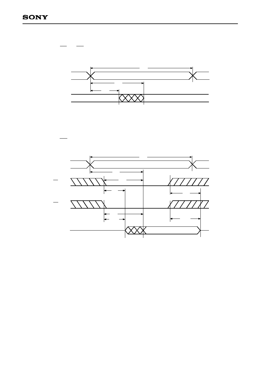
∑ Read cycle
Transition is measured ±200mV from steady voltage with specified loading in Fig. 1 1-(2).
This parameter is sampled and is not 100% tested.
∑ Write cycle
Transition is measured ±200mV from steady voltage with specified loading in Fig. 1 1-(2).
This parameter is sampled and is not 100% tested.
t
RC
t
AA
t
CO
t
OE
t
OH
t
LZ
t
OLZ
t
HZ
t
OHZ
12
--
--
--
3
3
0
0
0
--
12
12
6
--
--
--
6
6
ns
ns
ns
ns
ns
ns
ns
ns
ns
Read cycle time
Address access time
Chip enable access time
Output enable to output valid
Output data hold time
Chip enable to output in low Z (CE)
Output enable to output in low Z (OE)
Chip disable to output in high Z (CE)
Output disable to output in high Z (OE)
Item
Symbol
Unit
-12
Min.
Max.
t
WC
t
AW
t
CW
t
DW
t
DH
t
WP
t
AS
t
WR
t
OW
t
WHZ
12
10
10
8
0
10
0
0
4
0
--
--
--
--
--
--
--
--
--
6
ns
ns
ns
ns
ns
ns
ns
ns
ns
ns
Write cycle time
Address valid to end of write
Chip enable to end of write
Data valid to end of write
Data hold from end of write
Write pulse width
Address set up time
Write recovery time
Output active from lend of write
Write to output in high Z
Item
Symbol
Unit
-12
Min.
Max.
≠ 5 ≠
CXK5B41020TM
Timing Waveform
Address
t
AA
∑ Read cycle (1) : OE=V
IL
, WE=V
IH
t
RC
t
OH
Data out
Previous data valid
Data valid
Address
t
AA
t
RC
t
CO
t
LZ
t
HZ
t
OHZ
t
OE
t
OLZ
CE
OE
Data out
High impedance
Data valid
∑ Read cycle (2) : WE=V
IH