≠ 1 ≠
CXK5T8512TM/TN
-10LLX/12LLX
PE96727-PS
65536-word
◊
8-bit High Speed CMOS Static RAM
Description
The CXK5T8512TM/TN is a high speed CMOS
static RAM organized as 65536-words by 8-bits.
Special feature are low power consumption and
high speed.
The CXK5T8512TM/TN is a suitable RAM for
portable equipment with battery back up.
Features
∑ Extended operating temperature range:
≠25 to +85∞C
∑ Wide supply voltage range operation: 2.7 to 3.6V
∑ Fast access time:
(Access time)
3.0V operation
CXK5T8512TM/TN-10LLX 100ns (Max.)
CXK5T8512TM/TN-12LLX 120ns (Max.)
3.3V operation
CXK5T8512TM/TN-10LLX
85ns (Max.)
CXK5T8512TM/TN-12LLX 100ns (Max.)
∑ Low standby current:
14µA (Max.)
∑ Low data retention current: 12µA (Max.)
∑ Low power data retention:
2.0V
(Min.)
∑ Package line-up
CXK5T8512TM
8mm
◊
20mm 32 pin TSOP package
CXK5T8512TN
8mm
◊
13.4mm 32 pin TSOP package
Function
65536-word
◊
8-bit static RAM
Structure
Silicon gate CMOS IC
Sony reserves the right to change products and specifications without prior notice. This information does not convey any license by
any implication or otherwise under any patents or other right. Application circuits shown, if any, are typical examples illustrating the
operation of the devices. Sony cannot assume responsibility for any problems arising out of the use of these circuits.
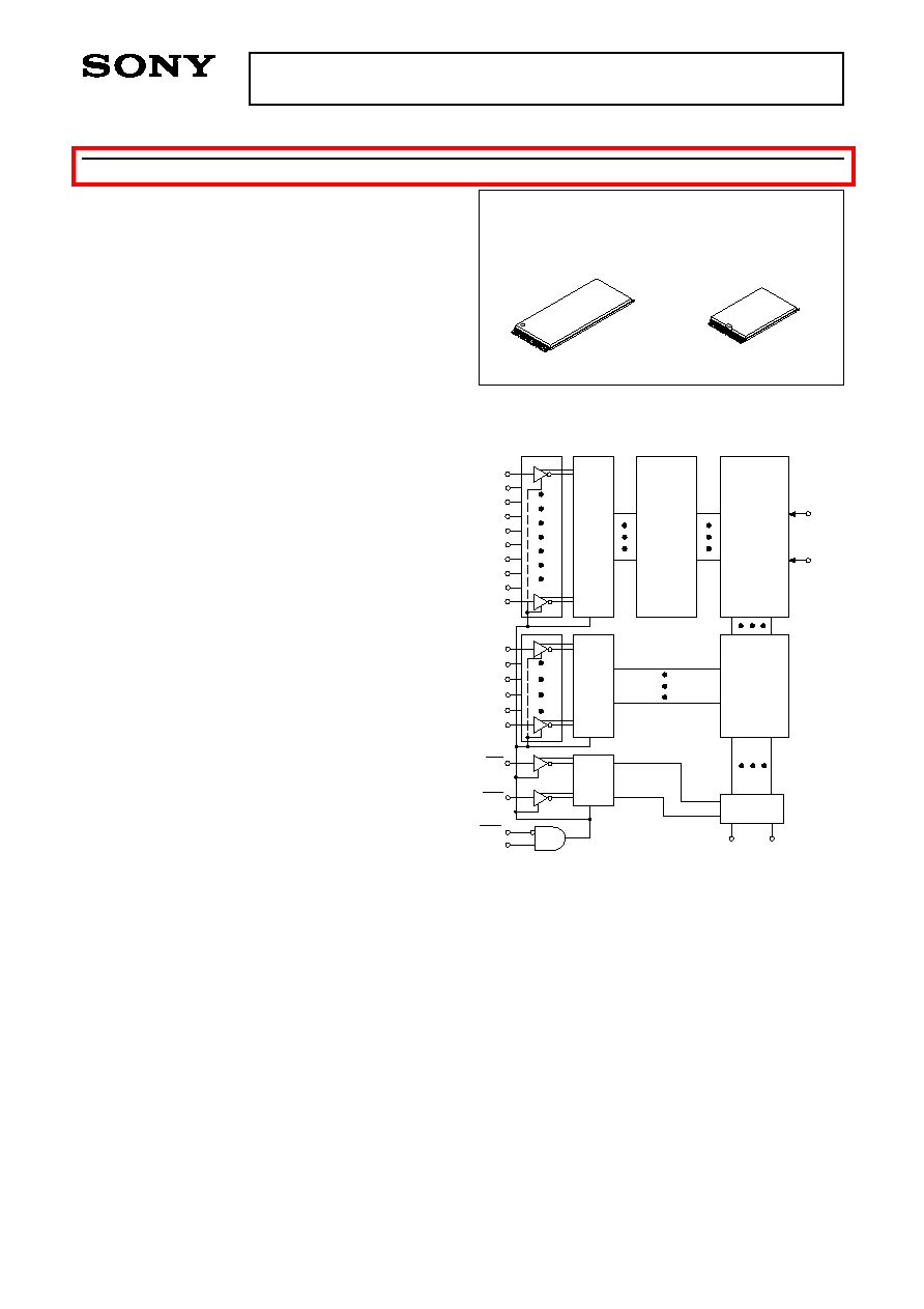
V
CC
GND
CE1
CE2
Row
Decoder
Buffer
Buffer
I/O Buffer
A15
A13
A8
A11
A9
A7
A6
A5
A14
A12
A4
A3
A10
A0
A1
OE
WE
Buffer
I/O Gate
Column
Decoder
Memory
Matrix
1024
◊
512
A2
I/O1
I/O8
Block Diagram
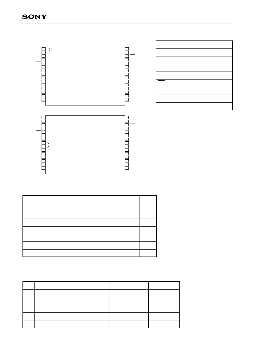
CXK5T8512TM
32 pin TSOP (Plastic)
CXK5T8512TN
32 pin TSOP (Plastic)
Preliminary
For the availability of this product, please contact the sales office.
≠ 2 ≠
CXK5T8512TM/TN
Address input
Data input output
Chip enable 1, 2 input
Write enable input
Output enable input
Power supply
Ground
No connection
Symbol
Description
Supply voltage
Input voltage
Input and output voltage
Allowable power dissipation
Operating temperature
Storage temperature
Soldering temperature ∑ time
V
CC
V
IN
V
I/O
P
D
Topr
Tstg
Tsolder
≠0.5 to +4.6
≠0.5
1
to V
CC
+ 0.5
≠0.5
1
to V
CC
+ 0.5
0.7
≠25 to +85
≠55 to +150
235 ∑ 10
V
V
V
W
∞C
∞C
∞C ∑ s
Item
Symbol
Rating
Unit
Absolute Maximum Ratings
(Ta = 25∞C, GND = 0V)
1
V
IN
, V
I/O
= ≠3.0V Min. for pulse width less than 50ns.
Pin Description
A0 to A15
I/O1 to I/O8
CE1, CE2
WE
OE
V
CC
GND
NC
OE
A10
CE1
I/O8
I/O7
I/O6
I/O5
I/O4
GND
I/O3
I/O2
I/O1
A0
A1
A2
A3
A11
A9
A8
A13
WE
CE2
A15
Vcc
NC
NC
A14
A12
A7
A6
A5
A4
1
2
3
4
5
6
7
8
9
10
11
12
13
14
15
16
18
19
20
21
22
23
24
25
26
27
28
29
30
32
31
17
CXK5T8512TM
(Standard Pinout)
Pin Configuration (Top View)
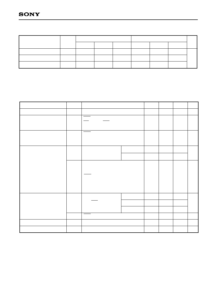
H
◊
L
L
L
◊
L
H
H
H
◊
◊
H
L
◊
◊
◊
H
H
L
Not selected
Not selected
Output disable
Read
Write
High Z
High Z
High Z
Data out
Data in
I
SB1
, I
SB2
I
SB1
, I
SB2
I
CC1
, I
CC2
, I
CC3
I
CC1
, I
CC2
, I
CC3
I
CC1
, I
CC2
, I
CC3
CE1 CE2
OE
WE
Mode
I/O pin
V
CC
Current
Truth Table
◊
: "H" or "L"
OE
A10
CE1
I/O8
I/O7
I/O6
I/O5
I/O4
GND
I/O3
I/O2
I/O1
A0
A1
A2
A3
A11
A9
A8
A13
WE
CE2
A15
Vcc
NC
NC
A14
A12
A7
A6
A5
A4
1
2
3
4
5
6
7
8
9
10
11
12
13
14
15
16
18
19
20
21
22
23
24
25
26
27
28
29
30
32
31
17
CXK5T8512TN
(Standard Pinout)
≠ 3 ≠
CXK5T8512TM/TN
DC Recommended Operating Conditions
(Ta = ≠25 to +85∞C, GND = 0V)
1
V
IL
= ≠3.0V Min. for pulse width less than 50ns.
Input leakage current
Output leakage current
Operating power supply
current
I
LI
I
LO
I
CC1
V
IN
= GND to V
CC
CE1 = V
IH
or CE2 = V
IL
or
OE = V
IH
or WE = V
IL
V
I/O
= GND to V
CC
CE1 = V
IL
, CE2 = V
IH
V
IN
= V
IH
or V
IL
I
OUT
= 0mA
10LLX
12LLX
≠25 to +85∞C
≠25 to +70∞C
+25∞C
≠1
≠1
--
--
--
--
5
10
--
--
--
--
--
--
0.24
0.12
14
7
--
1.4
µA
mA
--
--
1
25
2
25
+1
+1
3
35
3
35
µA
µA
mA
mA
mA
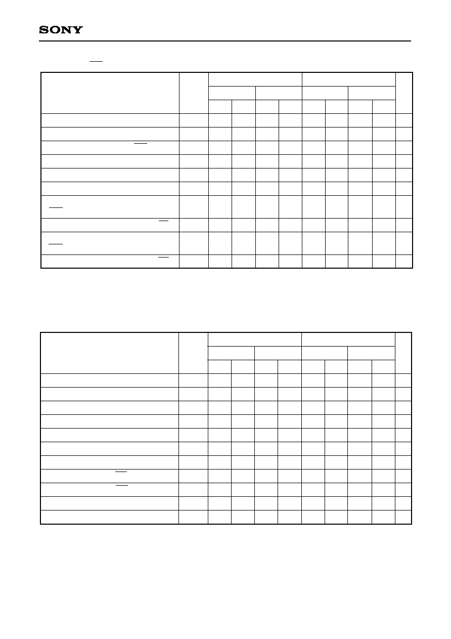
Item
Symbol
Min.
Typ.
1
Max.
Unit
Test conditions
Electrical Characteristics
∑ DC Characteristics
(V
CC
= 2.7 to 3.6V, GND = 0V, Ta = ≠25 to +85∞C)
1
V
CC
= 3.3V, Ta = 25∞C
2
I
CC2
= 30mA for 3.3V operation (V
CC
= 3.3V ± 0.3V)
3
I
CC2
= 40mA for 3.3V operation (V
CC
= 3.3V ± 0.3V)
Average operating current
Output high voltage
Output low voltage
Standby current
I
CC2
I
CC3
I
SB1
I
SB2
V
OH
V
OL
Min. cycle
duty = 100%
I
OUT
= 0mA
Cycle time 1µs
duty = 100%
I
OUT
= 0mA
CE1
0.2V
CE2
Vcc ≠ 0.2V
V
IL
0.2V
V
IH
Vcc ≠ 0.2V
CE1 = V
IH
or CE2 = V
IL
I
OL
= 2.0mA
2.4
--
--
--
--
0.4
V
V
I
OH
= ≠2.0mA
CE2
0.2V
CE1
Vcc ≠ 0.2V
or
{
CE2
Vcc ≠ 0.2V
Supply voltage
Input high voltage
Input low voltage
Item
Symbol
Min.
V
CC
= 2.7 to 3.6V
V
CC
= 3.3V ± 0.3V
Typ.
Max.
Unit
V
CC
V
IH
V
IL
2.7
2.4
≠0.3
1
3.3
--
--
3.6
V
CC
+ 0.3
0.4
Min.
Typ.
Max.
3.0
2.2
≠0.3
1
3.3
--
--
3.6
V
CC
+ 0.3
0.6
V
≠ 4 ≠
CXK5T8512TM/TN
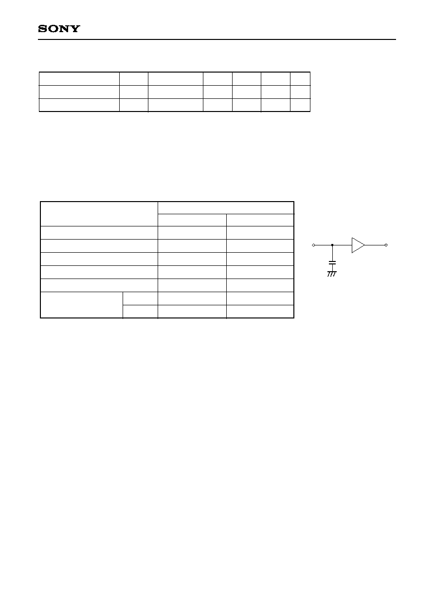
Input capacitance
I/O capacitance
Item
Symbol Test conditions
Min.
Typ.
Max.
Unit
C
IN
C
I/O
--
--
--
--
8
10
pF
pF
V
IN
= 0V
V
I/O
= 0V
AC Characteristics
∑ AC test conditions
(Ta = ≠25 to +85∞C)
I/O capacitance
(Ta = 25∞C, f = 1MHz)
Note) This parameter is sampled and is not 100% tested.
TTL
C
L
∑ Test circuit
Input pulse high level
Input pulse low level
Input rise time
Input fall time
Input and output reference level
-10LLX
Output load conditions
-12LLX
V
IH
= 2.4V
V
IL
= 0.4V
t
r = 5ns
t
f = 5ns
1.4V
C
L
1
= 100pF, 1TTL
C
L
1
= 100pF, 1TTL
Item
V
CC
= 2.7 to 3.6V
Conditions
V
IH
= 2.2V
V
IL
= 0.6V
t
r = 5ns
t
f = 5ns
1.4V
C
L
1
= 30pF, 1TTL
C
L
1
= 100pF, 1TTL
V
CC
= 3.3V ± 0.3V
1
C
L
includes scope and jig capacitances.
≠ 5 ≠
CXK5T8512TM/TN
∑ Read cycle (WE = "H")
1
t
HZ1
, t
HZ2
and t
OHZ
are defined as the time required for outputs to turn to high impedance state and are not
referred to as output voltage levels.
2
t
WHZ
is defined as the time required for outputs to turn to high impedance state and is not referred to as
output voltage level.
∑ Write cycle
Item
Symbol
Min.
Max.
Min.
Max.
-10LLX
V
CC
= 2.7 to 3.6V
V
CC
= 3.3V ± 0.3V
-12LLX
Unit
t
RC
t
AA
t
CO1
t
CO2
t
OE
t
OH
t
LZ1
t
LZ2
t
OLZ
t
HZ1
1
t
HZ2
1
t
OHZ
1
100
--
--
--
--
10
10
5
--
--
--
100
100
100
50
--
--
--
40
35
120
--
--
--
--
10
10
5
--
--
--
120
120
120
60
--
--
--
40
35
Min.
Max.
Min.
Max.
-10LLX
-12LLX
85
--
--
--
--
10
10
5
--
--
--
85
85
85
40
--
--
--
35
30
100
--
--
--
--
10
10
5
--
--
--
100
100
100
50
--
--
--
40
35
Read cycle time
Address access time
Chip enable access time (CE1)
Chip enable access time (CE2)
Output enable to output valid
Output hold from address change
Chip enable to output in low Z
(CE1, CE2)
Output enable to output in low Z (OE)
Chip disable to output in high Z
(CE1, CE2)
Output disable to output in high Z (OE)
ns
ns
ns
ns
ns
ns
ns
ns
ns
ns
Item
Symbol
Min.
Max.
Min.
Max.
-10LLX
V
CC
= 2.7 to 3.6V
V
CC
= 3.3V ± 0.3V
-12LLX
Unit
t
WC
t
AW
t
CW
t
DW
t
DH
t
WP
t
AS
t
WR
t
WR1
t
OW
t
WHZ
2
100
80
80
40
0
70
0
5
5
5
--
--
--
--
--
--
--
--
--
--
--
40
120
100
100
50
0
70
0
5
5
5
--
--
--
--
--
--
--
--
--
--
--
40
Min.
Max.
Min.
Max.
-10LLX
-12LLX
85
70
70
35
0
60
0
5
5
5
--
--
--
--
--
--
--
--
--
--
--
35
100
80
80
40
0
70
0
5
5
5
--
--
--
--
--
--
--
--
--
--
--
40
Write cycle time
Address valid to end of write
Chip enable to end of write
Data to write time overlap
Data hold from write time
Write pulse width
Address setup time
Write recovery time (WE)
Write recovery time (CE1, CE2)
Output active from end of write
Write to output in high Z
ns
ns
ns
ns
ns
ns
ns
ns
ns
ns
ns