16Mb LW R-L and 8Mb LW R-L w/ EC, rev 1.1
1 / 25
March 2, 2001
CXK77P36E160GB / CXK77P18E160GB
SONY
Æ
4/42/43/44
16Mb LW R-L HSTL High Speed Synchronous SRAMs (512K x 36 or 1M x 18)
8Mb LW R-L w/ EC HSTL High Speed Synchronous SRAMs (256K x 36 or 512K x 18)
Preliminary
Description
Features
∑
4 Speed Bins
Cycle Time / Access Time
-4 (-4A) (-4B)
4.0ns / 3.9ns (3.8ns) (3.7ns)
-42 (-42A) (-42B)
4.2ns / 4.2ns (4.1ns) (4.0ns)
-43 (-43A) (-43B)
4.3ns / 4.5ns (4.4ns) (4.3ns)
-44
4.4ns / 4.7ns
∑ Single 3.3V power supply (V
DD
): 3.3V
±
5%
∑ Dedicated output supply voltage (V
DDQ
): 1.9V typical
∑ HSTL-compatible I/O interface with dedicated input reference voltage (V
REF
): 0.85V typical
∑ Register - Latch (R-L) read operations
∑ Late Write (LW) write operations
∑ Conventional 16Mb or Error-Correcting (EC) 8Mb mode of operation, selectable via dedicated mode pin (M2)
∑ Full read/write coherency
∑ Byte Write capability
∑ One cycle deselect
∑ Differential input clocks (K/K)
∑ Programmable impedance output drivers
∑ Sleep (power down) mode via dedicated mode pin (ZZ)
∑ JTAG boundary scan (subset of IEEE standard 1149.1)
∑ 119 pin (7x17), 1.27mm pitch, 14mm x 22mm Ball Grid Array (BGA) package
The CXK77P36E160GB (organized as 524,288 words by 36 bits) and the CXK77P18E160GB (organized as 1,048,576 words
by 18 bits) are high speed CMOS synchronous static RAMs with common I/O pins. These synchronous SRAMs integrate input
registers, high speed RAM, output latches, and a one-deep write buffer onto a single monolithic IC. Register - Latch (R-L) read
operations and Late Write (LW) write operations are supported, providing a high-performance user interface.
Two distinct R-L modes of operation are supported, selectable via the M2 mode pin. When M2 is "high", these devices function
as conventional 16Mb R-L SRAMs, and pin 2B functions as a conventional SA address input. When M2 is "low", these devices
function as Error-Correcting (EC) 8Mb R-L SRAMs, and pin 2B is ignored.
When Error-Correcting 8Mb R-L mode is selected, the SRAM is divided into two banks internally - a "primary" bank and a
"secondary" bank. During write operations, input data is ultimately written to both banks internally (through one stage of write
pipelining). During read operations, data is read from both banks internally, and each byte of primary bank data is individually
parity-checked. If the parity of a particular byte of primary data is correct (that is, "odd"), it is driven valid externally. If the
parity of a particular byte of primary data is incorrect (that is, "even"), it is discarded, and the corresponding byte of secondary
bank data is driven valid externally. Primary / secondary bank data selection is performed on each data byte independently.
Data read from the secondary bank is NOT parity-checked.
Data read from the write buffer is NOT parity-checked.
All address and control input signals except ZZ (Sleep Mode) are registered on the rising edge of K (Input Clock).
During read operations, output data is driven valid from the falling edge of K, one half clock cycle after the address is registered.
During write operations, input data is registered on the rising edge of K, one full clock cycle after the address is registered.
The output drivers are series terminated, and the output impedance is programmable through an external impedance matching
resistor RQ. By connecting RQ between ZQ and V
SS
, the output impedance of all DQ pins can be precisely controlled.
Sleep (power down) mode control is provided through the asynchronous ZZ input. 250 MHz operation is obtained from a single
3.3V power supply. JTAG boundary scan interface is provided using a subset of IEEE standard 1149.1 protocol.

SONY
Æ
CXK77P36E160GB / CXK77P18E160GB
Preliminary
16Mb LW R-L and 8Mb LW R-L w/ EC, rev 1.1
2 / 25
March 2, 2001
512K x 36 Pin Assignment (Top View)
Notes:
1. Pad Locations 2T and 6T are true no-connects. However, they are defined as SA address inputs in x18 LW SRAMs.
2. Pad Location 6U must be left unconnected. It is used by Sony for internal test purposes.
3. Pad Location 3R is defined as an M1 mode pin in LW SRAMs. However, it must be tied "high" in this device.
4. Pad Location 5R is defined as an M2 mode pin in this device. It must be tied "high" or "low". When M2 is tied
"high", this device functions as a conventional 16Mb R-L SRAM. When M2 is tied "low", this device functions
as an Error-Correcting 8Mb R-L SRAM.
5. Pad Location 2B is defined as an SA address input in 16Mb LW SRAMs. However, it functions as a conventional
SA address input in this device only when M2 is tied "high". It is ignored in this device when M2 is tied "low".
6. Pad Location 4F is defined as a G output enable input in LW SRAMs. However, it must be tied "low" in this device.
1
2
3
4
5
6
7
A
V
DDQ
SA
SA
NC
SA
SA
V
DDQ
B
NC
SA
(5)
SA
NC
SA
SA
NC
C
NC
SA
SA
V
DD
SA
SA
NC
D
DQc
DQc
V
SS
ZQ
V
SS
DQb
DQb
E
DQc
DQc
V
SS
SS
V
SS
DQb
DQb
F
V
DDQ
DQc
V
SS
G
(6)
V
SS
DQb
V
DDQ
G
DQc
DQc
SBWc
NC
SBWb
DQb
DQb
H
DQc
DQc
V
SS
NC
V
SS
DQb
DQb
J
V
DDQ
V
DD
V
REF
V
DD
V
REF
V
DD
V
DDQ
K
DQd
DQd
V
SS
K
V
SS
DQa
DQa
L
DQd
DQd
SBWd
K
SBWa
DQa
DQa
M
V
DDQ
DQd
V
SS
SW
V
SS
DQa
V
DDQ
N
DQd
DQd
V
SS
SA
V
SS
DQa
DQa
P
DQd
DQd
V
SS
SA
V
SS
DQa
DQa
R
NC
SA
M1
(3)
V
DD
M2
(4)
SA
NC
T
NC
NC
(1)
SA
SA
SA
NC
(1)
ZZ
U
V
DDQ
TMS
TDI
TCK
TDO
RSVD
(2)
V
DDQ
SONY
Æ
CXK77P36E160GB / CXK77P18E160GB
Preliminary
16Mb LW R-L and 8Mb LW R-L w/ EC, rev 1.1
3 / 25
March 2, 2001
1M x 18 Pin Assignment (Top View)
Notes:
1a. Pad Location 4T is a true no-connect. However, it is defined as an SA address input in x36 LW SRAMs.
1b. Pad Locations 2D, 7D, 1E, 6E, 2F, 1G, 6G, 2H, 7H, 1K, 6K, 2L, 7L, 6M, 2N, 7N, 1P, and 6P are true no-connects.
However, they are defined as DQ data inputs / outputs in x36 LW SRAMs.
2. Pad Location 6U must be left unconnected. It is used by Sony for internal test purposes.
3. Pad Location 3R is defined as an M1 mode pin in LW SRAMs. However, it must be tied "high" in this device.
4. Pad Location 5R is defined as an M2 mode pin in this device. It must be tied "high" or "low". When M2 is tied
"high", this device functions as a conventional 16Mb R-L SRAM. When M2 is tied "low", this device functions
as an Error-Correcting 8Mb R-L SRAM.
5. Pad Location 2B is defined as an SA address input in 16Mb LW SRAMs. However, it functions as a conventional
SA address input in this device only when M2 is tied "high". It is ignored in this device when M2 is tied "low".
6. Pad Location 4F is defined as a G output enable input in LW SRAMs. However, it must be tied "low" in this device.
1
2
3
4
5
6
7
A
V
DDQ
SA
SA
NC
SA
SA
V
DDQ
B
NC
SA
(5)
SA
NC
SA
SA
NC
C
NC
SA
SA
V
DD
SA
SA
NC
D
DQb
NC
(1b)
V
SS
ZQ
V
SS
DQa
NC
(1b)
E
NC
(1b)
DQb
V
SS
SS
V
SS
NC
(1b)
DQa
F
V
DDQ
NC
(1b)
V
SS
G
(6)
V
SS
DQ6a
V
DDQ
G
NC
(1b)
DQb
SBWb
NC
V
SS
NC
(1b)
DQa
H
DQb
NC
(1b)
V
SS
NC
V
SS
DQa
NC
(1b)
J
V
DDQ
V
DD
V
REF
V
DD
V
REF
V
DD
V
DDQ
K
NC
(1b)
DQb
V
SS
K
V
SS
NC
(1b)
DQa
L
DQb
NC
(1b)
V
SS
K
SBWa
DQa
NC
(1b)
M
V
DDQ
DQb
V
SS
SW
V
SS
NC
(1b)
V
DDQ
N
DQb
NC
(1b)
V
SS
SA
V
SS
DQa
NC
(1b)
P
NC
(1b)
DQb
V
SS
SA
V
SS
NC
(1b)
DQa
R
NC
SA
M1
(3)
V
DD
M2
(4)
SA
NC
T
NC
SA
SA
NC
(1a)
SA
SA
ZZ
U
V
DDQ
TMS
TDI
TCK
TDO
RSVD
(2)
V
DDQ
SONY
Æ
CXK77P36E160GB / CXK77P18E160GB
Preliminary
16Mb LW R-L and 8Mb LW R-L w/ EC, rev 1.1
4 / 25
March 2, 2001
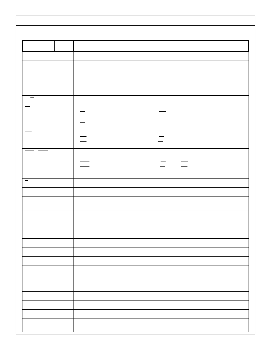
Pin Description
Symbol
Type
Description
SA
Input
Synchronous Address Inputs - Registered on the rising edge of K.
DQa, DQb
DQc, DQd
I/O
Synchronous Data Inputs / Outputs - Registered on the rising edge of K during write operations.
Driven from the falling edge of K during read operations.
DQa - indicates Data Byte a
DQb - indicates Data Byte b
DQc - indicates Data Byte c
DQd - indicates Data Byte d
K, K
Input
Differential Input Clocks
SS
Input
Synchronous Select Input - Registered on the rising edge of K.
SS = 0
specifies a write operation when SW = 0
specifies a read operation when SW = 1
SS = 1
specifies a deselect operation
SW
Input
Synchronous Global Write Enable Input - Registered on the rising edge of K.
SW = 0
specifies a write operation when SS = 0
SW = 1
specifies a read operation when SS = 0
SBWa, SBWb,
SBWc, SBWd
Input
Synchronous Byte Write Enable Inputs - Registered on the rising edge of K.
SBWa = 0 specifies write Data Byte a when SS = 0 and SW = 0
SBWb = 0 specifies write Data Byte b when SS = 0 and SW = 0
SBWc = 0 specifies write Data Byte c when SS = 0 and SW = 0
SBWd = 0 specifies write Data Byte d when SS = 0 and SW = 0
G
Input
Asynchronous Output Enable Input - Not supported. This control pin must be tied "low".
ZZ
Input
Asynchronous Sleep Mode Input - Asserted (high) forces the SRAM into low-power mode.
M1
Input
Read Operation Protocol Select 1 - This mode pin must be tied "high" to select Register - Latch
read operations.
M2
Input
Read Operation Protocol Select 2 - This mode pin must be tied "high" or "low".
M2 = 0
selects Error-Correcting 8Mb R-L functionality
M2 = 1
selects conventional 16Mb R-L functionality
ZQ
Input
Output Impedance Control Resistor Input
V
DD
3.3V Core Power Supply - Core supply voltage.
V
DDQ
Output Power Supply - Output buffer supply voltage.
V
REF
Input Reference Voltage - Input buffer threshold voltage.
V
SS
Ground
TCK
Input
JTAG Clock
TMS
Input
JTAG Mode Select
TDI
Input
JTAG Data In
TDO
Output
JTAG Data Out
RSVD
Reserved - This pin is used for Sony test purposes only. It must be left unconnected.
NC
No Connect - These pins are true no-connects, i.e. there is no internal chip connection to these
pins. They can be left unconnected or tied directly to V
DD
, V
DDQ
, or V
SS
.

SONY
Æ
CXK77P36E160GB / CXK77P18E160GB
Preliminary
16Mb LW R-L and 8Mb LW R-L w/ EC, rev 1.1
5 / 25
March 2, 2001
∑
Clock Truth Table
∑
Dynamic M2 Mode Pin State Changes
Although M2 is defined as a static input (that is, it must be tied "high" or "low" at power-up), in some instance (such as
during device testing) it may be desirable to change its state dynamically (that is, without first powering off the SRAM)
while preserving the contents of the memory array. If so, the following criteria must be met:
1. At least two (2) consecutive deselect operations must be initiated prior to changing the state of M2, to ensure that the
most recent read or write operation completes successfully.
2. At least thirty-two (32) consecutive deselect operations must be initiated after changing the state of M2 before any read
or write operations can be initiated, to allow the SRAM sufficient time to recognize the change in state.
∑
Sleep (Power Down) Mode
Sleep (power down) mode is provided through the asynchronous input signal ZZ. When ZZ is asserted (high), the output
drivers will go to a Hi-Z state, and the SRAM will begin to draw standby current. Contents of the memory array will be
preserved. An enable time (t
ZZE
) must be met before the SRAM is guaranteed to be in sleep mode, and a recovery time
(t
ZZR
) must be met before the SRAM can resume normal operation.
∑
Programmable Impedance Output Drivers
These devices have programmable impedance output drivers. The output impedance is controlled by an external resistor,
RQ, connected between the SRAM's ZQ pin and V
SS
, and is equal to one-fifth the value of this resistor, nominally. See
the DC Electrical Characteristics section for further information.
The output impedance is updated whenever the output drivers are in a Hi-Z state. Consequently, impedance updates will
occur during write and deselect operations. At power up, 8192 clock cycles followed by an impedance update via one of
the three methods described above are required to ensure that the output impedance has reached the desired value. After
power up, periodic impedance updates via write or deselect operations are also required to ensure that the output imped-
ance remains within specified tolerances.
∑
Power-Up Sequence
For reliability purposes, Sony recommends that power supplies power up in the following sequence: V
SS
, V
DD
, V
DDQ
,
V
REF
, and Inputs. V
DDQ
should never exceed V
DD
. If this power supply sequence cannot be met, a large bypass diode
may be required between V
DD
and V
DDQ
. Please contact Sony Memory Application Department for further information.
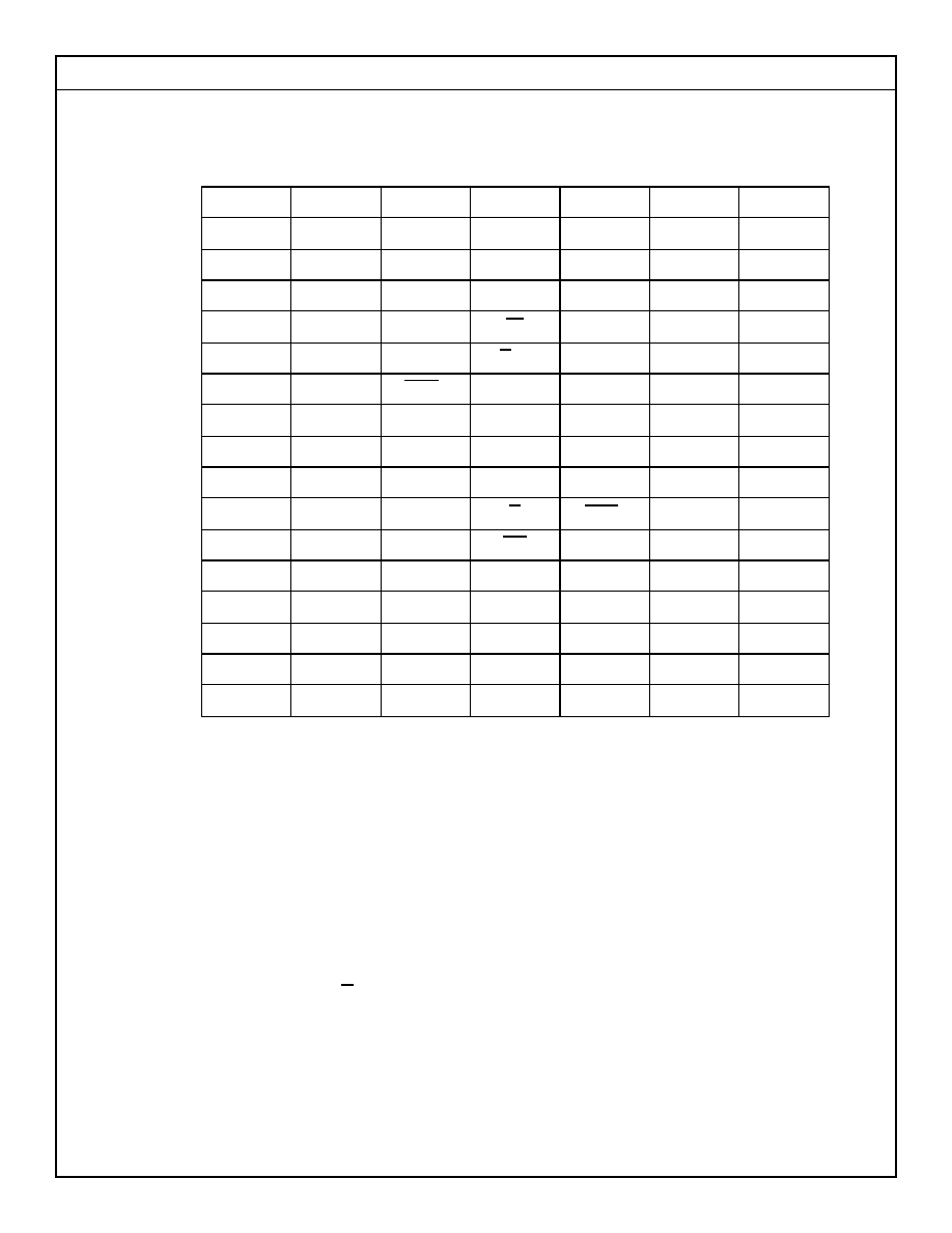
K
ZZ
SS
(t
n
)
SW
(t
n
)
SBWx
(t
n
)
Operation
DQ
(t
n
)
DQ
(t
n+1
)
X
H
X
X
X
Sleep (Power Down) Mode
Hi - Z
Hi - Z
L
H
L
H
X
X
Deselect
Hi - Z
X
L
H
L
L
H
X
Read
Q(t
n
)
X
L
H
L
L
L
L
Write All Bytes
Hi - Z
D(t
n
)
L
H
L
L
L
X
Write Bytes With SBWx = L
Hi - Z
D(t
n
)
L
H
L
L
L
H
Abort Write
Hi - Z
X