
18Mb 1x2Lp, HSTL, rev 1.1
1 / 25
November 8, 2002
SONY
RAM
TM
33/4/5
CXK79M36C162GB
18Mb 1x2Lp HSTL High Speed Synchronous SRAMs (512Kb x 36)
Preliminary
Description
The CXK79M36C162GB is a high speed CMOS synchronous static RAM with common I/O pins. It is manufactured in com-
pliance with the JEDEC-standard 209 pin BGA package pinout defined for SigmaRAM
TM
devices. It integrates input registers,
high speed RAM, output registers, and a two-deep write buffer onto a single monolithic IC. Double Data Rate (DDR) Pipelined
(PL) read operations and Late Write (LW) write operations are supported, providing a high-performance user interface. Positive
and negative output clocks are provided for applications requiring source-synchronous operation.
All address and control input signals are registered on the rising edge of the CK differential input clock.
During read operations, output data is driven valid twice, from both the rising and falling edges of CK, beginning one full cycle
after the address and control signals are registered.
During write operations, input data is registered twice, on both the rising and falling edges of CK, beginning one full cycle after
the address and control signals are registered.
Because two pieces of data are always transferred during read and write operations, the least significant address bit of the in-
ternal memory array is not available as an external address pin to this device. Consequently, the number of external address pins
available to the device is one less than the specified depth of the device (i.e. the 512Kb x 36 device has 18, not 19, external
address pins). And, the user cannot choose the order in which the two pieces of data are read. Read data is always provided in
the same order in which it is written.
Output drivers are series-terminated, and output impedance is programmable via the ZQ control pin. When an external resistor
RQ is connected between ZQ and V
SS
, the impedance of the SRAM's output drivers is set to ~RQ/5.
300 MHz operation (600 Mbps) is obtained from a single 1.8V power supply. JTAG boundary scan interface is provided using
a subset of IEEE standard 1149.1 protocol.
Features
�
3 Speed Bins
Cycle Time / Data Access Time
-33
3.3ns / 1.8ns
-4
4.0ns / 2.1ns
-5
5.0ns / 2.3ns
� Single 1.8V power supply (V
DD
): 1.7V (min) to 1.95V (max)
� Dedicated output supply voltage (V
DDQ
): 1.4V (min) to V
DD
(max)
� HSTL-compatible I/O interface with dedicated input reference voltage (V
REF
): V
DDQ
/2 typical
� Common I/O
� Double Data Rate (DDR) data transfers
� Pipelined (PL) read operations
� Late Write (LW) write operations
� Burst capability with internally controlled Linear Burst address sequencing
� Burst length of two or four, with automatic address wrap
� Full read/write data coherency
� Differential input clocks (CK and CK)
� Data-referenced output clocks (CQ1, CQ1, CQ2, CQ2)
� Programmable output driver impedance via dedicated control pin (ZQ)
� Depth expansion capability (2 or 4 banks) via programmable chip enables (E2, E3, EP2, EP3)
� JTAG boundary scan (subset of IEEE standard 1149.1)
� 209 pin (11x19), 1mm pitch, 14mm x 22mm Ball Grid Array (BGA) package

SONY
�
RAM
Preliminary
18Mb 1x2Lp, HSTL, rev 1.1
2 / 25
November 8, 2002
CXK79M36C162GB
512Kb x 36 Pin Assignment (Top View)
Notes:
1: Pin 6W is defined as Address Pin A0 in Single Data Rate (SDR) Common I/O SigmaRAMs. However, it must be tied "low"
in this device. The least significant address bit of the internal memory array is not available as an externally controlled ad-
dress pin in Double Data Rate (DDR) Common I/O SigmaRAMs.
2. Pins 3B, 4C, 8B, and 9C are defined as Byte Write Enable Pins Bx in x36 Single Data Rate (SDR) Common I/O Sigma-
RAMs. However, they must be tied "low" in this device. Byte Write functionality is not supported in Double Data Rate
(DDR) Common I/O SigmaRAMs.
1
2
3
4
5
6
7
8
9
10
11
A
NC
NC
A
E2
A
ADV
A
E3
A
DQ
DQ
B
NC
NC
MCL
(2)
NC
A
(x36)
W
A
MCL
(2)
NC
DQ
DQ
C
NC
NC
NC
MCL
(2)
NC
(144M)
E1
NC
NC
MCL
(2)
DQ
DQ
D
NC
NC
V
SS
V
REF
NC
MCL
NC
V
REF
V
SS
DQ
DQ
E
NC
DQ
V
DDQ
V
DDQ
V
DD
V
DD
V
DD
V
DDQ
V
DDQ
NC
DQ
F
DQ
DQ
V
SS
V
SS
V
SS
ZQ
V
SS
V
SS
V
SS
NC
NC
G
DQ
DQ
V
DDQ
V
DDQ
V
DD
EP2
V
DD
V
DDQ
V
DDQ
NC
NC
H
DQ
DQ
V
SS
V
SS
V
SS
EP3
V
SS
V
SS
V
SS
NC
NC
J
DQ
DQ
V
DDQ
V
DDQ
V
DD
MCH
V
DD
V
DDQ
V
DDQ
NC
NC
K
CQ2
CQ2
CK
CK
V
SS
MCL
V
SS
NC
NC
CQ1
CQ1
L
NC
NC
V
DDQ
V
DDQ
V
DD
MCL
V
DD
V
DDQ
V
DDQ
DQ
DQ
M
NC
NC
V
SS
V
SS
V
SS
MCH
V
SS
V
SS
V
SS
DQ
DQ
N
NC
NC
V
DDQ
V
DDQ
V
DD
MCH
V
DD
V
DDQ
V
DDQ
DQ
DQ
P
NC
NC
V
SS
V
SS
V
SS
MCL
V
SS
V
SS
V
SS
DQ
DQ
R
DQ
NC
V
DDQ
V
DDQ
V
DD
V
DD
V
DD
V
DDQ
V
DDQ
DQ
NC
T
DQ
DQ
V
SS
V
REF
NC
MCL
NC
V
REF
V
SS
NC
NC
U
DQ
DQ
NC
A
NC
(72M)
A
NC
(36M)
A
NC
NC
NC
V
DQ
DQ
A
A
A
A1
A
A
A
NC
NC
W
DQ
DQ
TMS
TDI
A
MCL
(1)
A
TDO
TCK
NC
NC

SONY
�
RAM
Preliminary
18Mb 1x2Lp, HSTL, rev 1.1
3 / 25
November 8, 2002
CXK79M36C162GB
Pin Description
Symbol
Type
Quantity
Description
A
Input
17
Address Inputs - Registered on the rising edge of CK.
A1
Input
1
Address Input 1 - Registered on the rising edge of CK. Initializes burst counter.
DQ
I/O
36
Data Inputs / Outputs - Registered on the rising and falling edges of CK during write
operations. Driven from the rising and falling edges of CK during read operations.
CK, CK
Input
2
Differential Input Clocks
CQ1, CQ1
CQ2, CQ2
Output
4
Output Clocks
E1
Input
1
Chip Enable Control Input - Registered on the rising edge of CK.
E1 = 0
enables the device to accept read and write commands.
E1 = 1
disables the device.
See the Clock Truth Table section for further information.
E2, E3
Input
2
Programmable Chip Enable Control Inputs - Registered on the rising edge of CK. See
the Clock Truth Table and Depth Expansion sections for further information.
EP2, EP3
Input
2
Programmable Chip Enable Active-Level Select Inputs - These pins must be tied
"high" or "low" at power-up. See the Clock Truth Table and Depth Expansion sec-
tions for further information.
ADV
Input
1
Address Advance Control Input - Registered on the rising edge of CK.
ADV = 0
loads a new address and begins a new operation when the device is
enabled.
ADV = 1
increments the address and continues the previous operation when the
device is enabled.
See the Clock Truth Table section for further information.
W
Input
1
Write Enable Control Input - Registered on the rising edge of CK.
W = 0
specifies a write operation when ADV = 0 and the device is enabled.
W = 1
specifies a read operation when ADV = 0 and the device is enabled.
See the Clock Truth Table section for further information.
ZQ
Input
1
Output Impedance Control Resistor Input - This pin must be tied to V
SS
through an
external resistor RQ at power-up. Output driver impedance is set to one-fifth the
value of RQ, nominally. See the Output Driver Impedance Control section for further
information.
V
DD
14
1.8V Core Power Supply - Core supply voltage.
V
DDQ
24
Output Power Supply - Output buffer supply voltage.
V
REF
4
Input Reference Voltage - Input buffer threshold voltage.
V
SS
30
Ground
TCK
Input
1
JTAG Clock
TMS
Input
1
JTAG Mode Select - Weakly pulled "high" internally.
TDI
Input
1
JTAG Data In - Weakly pulled "high" internally.
TDO
Output
1
JTAG Data Out
MCL
*Input*
10
Must Connect "Low" - May not be actual input pins.
MCH
*Input*
3
Must Connect "High" - May not be actual input pins.
NC
52
No Connect - These pins are true no-connects, i.e. there is no internal chip connection
to these pins. They can be left unconnected or tied directly to V
SS
.

SONY
�
RAM
Preliminary
18Mb 1x2Lp, HSTL, rev 1.1
4 / 25
November 8, 2002
CXK79M36C162GB
Clock Truth Table
Notes:
1. "1" = input "high"; "0" = input "low"; "X" = input "don't care"; "T" = input "true"; "F" = input "false".
2. "***" indicates that the DQ input requirement or output state and the CQ output state are determined by the previous operation.
3. If E2 = EP2 and E3 = EP3 then E = "T" else E = "F".
4. DQs are tri-stated in response to Bank Deselect, Deselect, and Write commands, one full cycle after the command is sampled.
5. CQs are tri-stated in response to Bank Deselect commands only, one full cycle after the command is sampled.
6. One (1) Continue operation may be initiated after a Read or Write operation is initiated to burst transfer four (4) distinct piec-
es of data per single external address input. If a second (2nd) Continue operation is initiated, the internal address wraps back
to the initial external (base) address.
CK
E1
(t
n
)
E
(t
n
)
ADV
(t
n
)
W
(t
n
)
Previous
Operation
Current Operation
DQ/CQ
(t
n
)
DQ/CQ
(t
n+�
)
DQ/CQ
(t
n+1
)
DQ/CQ
(t
n+1�
)
X
F
0
X
X
Bank Deselect
***
Hi-Z
X
X
1
X
Bank Deselect
Bank Deselect (Continue)
Hi-Z
Hi-Z
1
T
0
X
X
Deselect
***
Hi-Z/CQ
X
X
1
X
Deselect
Deselect (Continue)
Hi-Z/CQ
Hi-Z/CQ
0
T
0
0
X
Write
Loads new address
***
***
D1/CQ
D2/CQ
X
X
1
X
Write
Write Continue
Increments address by 2
D1/CQ
D2/CQ
D3/CQ
D4/CQ
0
T
0
1
X
Read
Loads new address
***
***
Q1/CQ
Q2/CQ
X
X
1
X
Read
Read Continue
Increments address by 2
Q1/CQ
Q2/CQ
Q3/CQ
Q4/CQ
SONY
�
RAM
Preliminary
18Mb 1x2Lp, HSTL, rev 1.1
5 / 25
November 8, 2002
CXK79M36C162GB
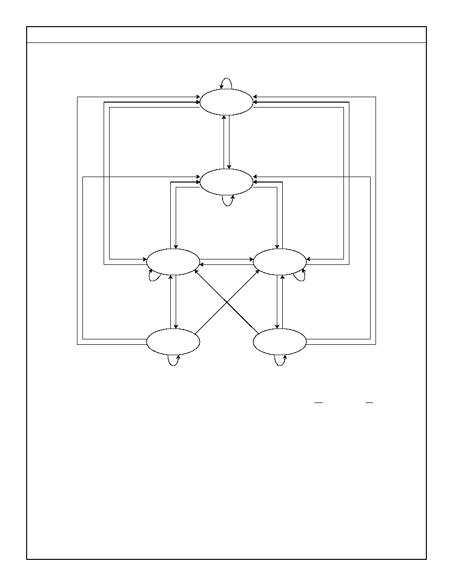
State Diagram
Notes:
1. The notation "X,X,X,X" controlling the state transitions above indicate the states of inputs E1, E, ADV, and W respectively.
2. "1" = input "high"; "0" = input "low"; "X" = input "don't care"; "T" = input "true"; "F" = input "false".
3. If E2 = EP2 and E3 = EP3 then E = "T" else E = "F".
Deselect
Bank
Deselect
Read
Read
Write
Write
Continue
X,F,0,X or X,X,1,X
Continue
X,F,0,X
1,T,0,X
X,F,0,X
1,T,0,X
1,T,0,X
X,F,0,X
1,T,0,X
1,T,0,X or X,X,1,X
0,T,0,0
0,T,0,1
0,T,0,0
0,T,0,1
X,F,0,X
X,F,0,X
0,T,0,0
0,T,0,1
X,X,1,X
X,X,1,X
0,T,0,0
0,T,0,1
1,T,0,X
0,T,0,0 0,T,0,1
X,X,1,X
X,X,1,X
0,T,0,1
0,T,0,0