 | –≠–Ľ–Ķ–ļ—ā—Ä–ĺ–Ĺ–Ĺ—č–Ļ –ļ–ĺ–ľ–Ņ–ĺ–Ĺ–Ķ–Ĺ—ā: CXL1008M | –°–ļ–į—á–į—ā—Ć:  PDF PDF  ZIP ZIP |
CMOS-CCD Signal Processor for Skew Compensation
Description
CXL1008M/P are CMOS-CCD signal processors
developed for the variable-speed video signal processor
for home-use 8mm VCRs.
Features
∑ Low power consumption 105mW (Typ.)
∑ Built-in peripheral circuit
∑ Adjustment is necessary for one part.
Structure
CMOS-CCD
Functions
∑ 1/2H 359-bit, direct 20-bit CCD register
∑ Clock driver
∑ Timing oscillation circuit
∑ Automatic bias circuit
∑ Sync tip clamp circuit
∑ Dummy VD insert circuit
∑ Sample/hold circuit
Absolute Maximum Ratings (Ta = 25įC)
∑ Supply voltage
V
DD
11
V
V
CL
6
V
∑ Operating temperature Topr
≠10 to +60
įC
∑ Storage temperature
Tstg
≠55 to +150
įC
∑ Allowable power dissipaiton
P
D
CXL1008M 500 mW
CXL1008P 1000 mW
Recommended Operating Conditions
Supply voltage
V
DD
9V Ī 5
%
V
CL
5V Ī 5
%
Recommended Clock Conditions
∑ Clock input amplitude
V
CLK
0.15 to 1.0 (0.3 Typ.)
Vp-p
∑ Clock frequency
f
CLK
10.738635
MHz
≠ 1 ≠
E60248-PS
Sony reserves the right to change products and specifications without prior notice. This information does not convey any license by
any implication or otherwise under any patents or other right. Application circuits shown, if any, are typical examples illustrating the
operation of the devices. Sony cannot assume responsibility for any problems arising out of the use of these circuits.
CXL1008M/P
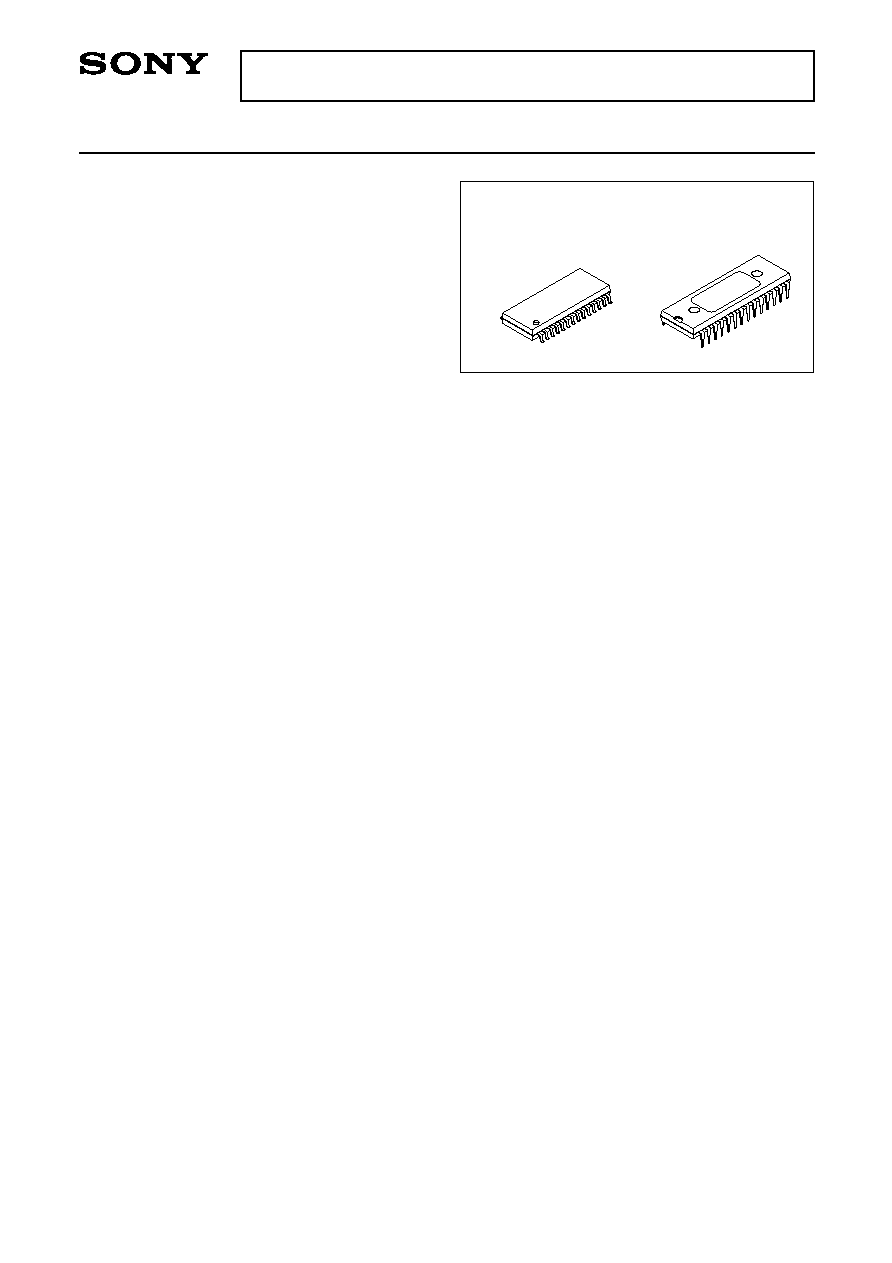
CXL1008M
28 pin SOP (Plastic)
CXL1008P
28 pin DIP (Plastic)
≠ 2 ≠
CXL1008M/P
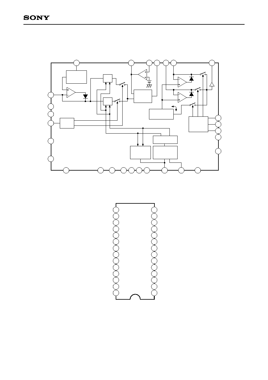
Block Diagram
2
3
4
5
6
7
8
9
10
11
12
13
14
1
15
16
17
18
19
20
21
22
23
24
25
26
27
28
SIG IN1
MUTE IN
T7
T2
T1
T8
EXT VD
JOG IN
V
CL
T6
CLK IN
T5
T4
T3
V
SS
V
SS
V
DD
REC/PB
AUTO
SIG IN2
SIG OUT
SIG DELAY
CCD OUT
FEED OUT
FEED IN
SKEW IN
T9
T10
OUTPUT
CONTROL
50mV
REFERENCE
50mV
OUTPUT
CIRCUIT
1/2H
D
AUTOBIAS
CIRCUIT
SKEW
DRIVER
TIMING
GENERATOR
DUTY
CONTROL
1
2
Pin Configuration (Top View)
2
3
4
5
6
7
8
9
10
11
12
13
14
15
16
17
18
19
20
21
22
23
24
25
26
27
28
1
V
CL
AUTO
SIG IN2
SIG IN1
MUTE IN
T7
T6
CLK IN
T5
T4
T3
T2
T1
V
SS
T8
EXT VD
JOG IN
V
SS
SIG OUT
V
DD
SIG DELAY
REC/PB
CCD OUT
FEED OUT
FEED IN
SKEW IN
T9
T10
≠ 3 ≠
CXL1008M/P
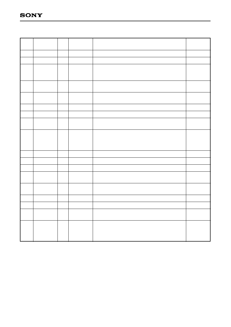
Pin Description
Pin
No.
1
7
10
11
12
13
14
16
17
18
19
20
21
22
23
24
25
26
V
SS
CLK IN
MUTE IN
SIG IN1
SIG IN2
AUTO
V
CL
EXT VD
JOG IN
V
SS
SIG OUT
V
DD
SIG DELAY
REC/PB
CCD OUT
FEED OUT
FEED IN
SKEW IN
I
I
I
I
O
I
I
O
I
I
O
O
I
I
0.3Vp-p
5V when
muting,
normally 0V
1.1Vp-p or
less
2.2Vp-p or
less
+5V
5V when VD
is inserted
JOG mode
5V
PB/REC
mode
0V
+9V
5V when PB
0V when REC
GND
Input the sine wave of 3fsc (10.738635MHz)
The video signal mute is generated at High level.
See the Logic Table of Signal Output Selection
State (Table 1).
Signal input pin of CCD DL.
Input composite video signal.
Signal input pin of the through side.
Input composite video signal.
The DC level of automatic bias is output.
Power supply 1
Use this pin when VD is inserted to the video signal
with the extrenal dummy VD signal input.
JOG/NORMAL PB selection pin.
See the Logic Table of Signal Output Selection
State (Table 1).
GND
Final output
Power supply 2
After the output from Pin 23 CCD OUT passes through
LPF, input it to the same pin and insert clamp and VD.
Operate the clock at High when PB.
Stop the clock at Low when REC.
Direct output from CCD DL
Feedback DC output
Smoothing capacitor connection pin of the bias
commutation loop on the output circuit
Select Direct DL and 1/2H DL signals when High
and Low, respectively.
See the Logic Table of CCD DL Mode Selection
(Table 2).
> 50k
> 100k
> 100k
> 100k
10k
> 100k
> 100k
0.6 to 1.5k
> 100k
> 100k
0.6 to 1.5k
10k
> 100k
> 100k
Symbol
I/O
Supply
voltage
Description
Impedance
(
)
Note) T1 through T10 test pins must be connected as shown in the application circuit because of the IC
internal circuit.
Notes on Handling
Countermeasures for electrostatics are necessary because some pins have low electrostatic strength
(particularly Pin 26: SKEW IN).
≠ 4 ≠
CXL1008M/P
Items
Power current
Clock input level
Signal input pin voltage
Signal output pin voltage
CCD signal output
voltage difference
Signal insert gain
CCD output signal gain
difference
Frequency characteristics
Frequency characteristics
difference
Differential gain
I
DD
I
CL
CLK
Vdi1
Vdi2
Vdi3
Vdo1
Vdo2
Dab
IG
CCD
IG
In2
IG
DL
Gab
f
CCD
f
In2
f
DL
fab
DG
CCD
DG
In2
DG
DL
PB, JOG
Direct
1/2H
Direct
1/2H
3.58MHz/100kHz
10MHz/100kHz
10MHz/100kHz
Direct
1/2H at 3.58MHz
1.1Vp-p input
2.2Vp-p input
2.2Vp-p input
c
c
c
b
a
c
b
c
c
b
a
c
c
b
a
c
c
b
a
a
a
a
a
a
a
a
a
b
b
b
b
b
b
b
b
b
b
b
a
a
e
e
e
e
e
e
a
f
f
a
b
c
b
d
b
d
b
c
g
g
g
a
a
b
b
a
a
b
b
a
a
b
b
a
a
a
a
a
b
b
b
b
c
c
c
L
L
L
L
L
L
L
L
L
L
L
L
L
L
L
L
H
L
H
L
H
H
H
H
H
H
H
H
H
H
H
H
H
L
H
L
H
L
0.15
4.0
4.0
4.0
1.7
1.5
≠55
≠3.0
≠1.2
≠1.2
≠1.3
≠3
≠0.5
≠0.5
≠0.2
0
0
0
7
8
0.3
5.0
4.2
4.2
2.0
2.0
0
0
≠0.8
≠0.8
0
≠2
0
0
0
3
2
2
12
10
1.0
6.0
4.4
4.4
2.4
2.5
55
3.0
0
0
1.3
0
--
--
0.2
10
4
4
mA
mA
V
V
V
V
V
V
mV
dB
dB
dB
%
dB
dB
dB
dB
%
%
%
1
1
2
2
2
3
3
4
5
5
5
6
7
8
8
9
10
10
10
Symbol
Test Conditions
Switch Conditions
Control Pin Conditions
1
,
2
Min.
Typ.
Max.
Unit
Note
1
2
3
4
5
P1
P2
P3
P4
P5
Electrical Characteristics
(See the Electrical Characteristics Test Circuit)
(Ta = 25įC, V
DD
= 9.0V, V
CL
= 5.0V, f
CLK
= 10.7MHz, V
CLK
= 0.3Vp-p sine wave)
≠ 5 ≠
CXL1008M/P
Items
Differential phase
Allowable input amplitude
S/N rate
VD insert depth
Logical input
DP
CCD
DP
In2
DP
DL
V
IN1≠AC
V
IN2≠AC
S/N
CCD
S/N
In2
S/N
DL
V
VD
V
IN H
V
IN L
1.1Vp-p input
2.2Vp-p input
2.2Vp-p input
2Vp-p video signal from
sync tip
c
b
a
c
a/b
c
b
a
a
b
b
b
b
b
b
a
g
g
g
g
g
a
e
f
e
f
e
g
a
b
b
a
b
b
b
c
c
c
d
d
d
a
L
L
L
L
L
L
L
L
L
L
H
L
H
H
H
H
0
0
0
--
--
50
50
50
0
4.0
--
3
3
3
--
--
55
65
65
50
5
5
5
1.1
2.2
--
--
--
100
--
1.0
deg
deg
deg
Vp-p
Vp-p
dB
dB
dB
mV
V
V
10
10
10
11
11
11
12
Symbol
Test Conditions
Switch Conditions
Control Pin Conditions
1
,
2
Min.
Typ.
Max.
Unit
Note
1
2
3
4
5
P1
P2
P3
P4
P5
1
Control pins correspond to P1 through P5 of the Electrical Characteristics Test Circuit.
2
Symbols "H" and "L" in control pin conditions represent "V
IN H
" and "V
IN L
" of logical input.

≠ 6 ≠
CXL1008M/P
P2
P3
P5
2
3
4
5
6
7
8
9
10
1
a
SW5
b
c
d
11
12
13
14
15
16
17
18
19
20
21
22
23
24
25
26
27
28
0.1Ķ
V3
22Ķ
10k
10Ķ
220k
P4
5V
2SA1175
9V
2SA1175
2k
A2
9V
V2
2k
5V
390k
SW4
a
b
0.1Ķ
◊
1
LPF
BPF
Note 1)
Note 2)
◊
1
0.1Ķ
◊
1
◊
1
OSCILLOSCOPE
SPECTRUM
ANALYZER
VECTOR SCOPE
NOISE METER
100k
5V
CLK
P1
5V
10Ķ
A1
SW1
a
b
c
V1
SW2
a
b
20k
1M
V
BIAS
0.1Ķ
SW3
a
b
c
d
e
f
g
100kHz 1.1Vp-p SINE WAVE
100kHz 300mVp-p SINE WAVE
3.58MHz 300mVp-p SINE WAVE
10MHz 300mVp-p SINE WAVE
GROUND
100kHz 2.2Vp-p SINE WAVE
5-STAIR CASE WAVE
0
5.8
10.7
Frequency [MHz]
≠50
≠3
0
Note 1) LPF Frequency Response
(Delay Time to 140ns)
0
4.1M
10.7M
Frequency [Hz]
≠50
≠3
0
50
[dB]
[dB]
Note 2) BPF Frequency Response
200
Electrical Characteristics Test Circuit
≠ 7 ≠
CXL1008M/P
Notes)
1) Current value when the clock is in operation in the PB or JOG mode.
In the REC mode, the clock is stopped (Pin 22 is at low) to save power.
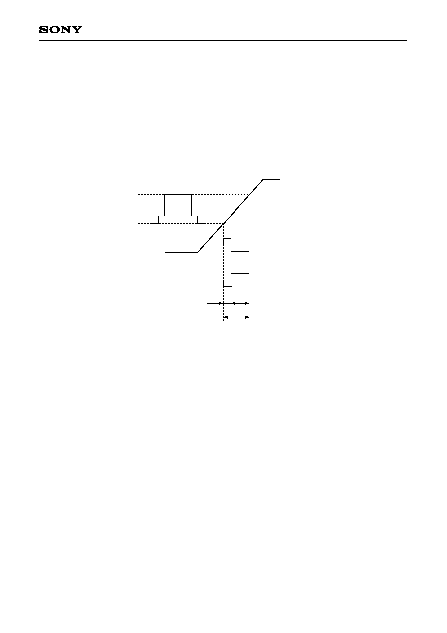
2) With the signal input pin voltage value, the video signal sync tip is clamped.
3) Vdo1 is a CCD OUT output voltage when the SIG IN1 input voltage is Vdi1.
Vdo2 is a SIG OUT output voltage when the SIG IN2 input voltage is Vdi2.
Vdo1 and Vdo2 represent outputs for the sync tip clamp level when a white level signal is input as shown
in the diagram.
1.0Vp-p
100%
40%
Vdi
Input signal
Vdo
Output signal
4)
Dab denotes an output voltage difference of CCD OUT when the direct DL and 1/2H DL are switched.
5) IG
CCD
is a CCD OUT gain when a 1.1Vp-p 100kHz sine wave is input to SIG IN1.
IG
CCD
= 20 log
Output amplitude (Vp-p)
1.1Vp-p
It is measured by giving a Vdi1 + 0.6 bias with V
Bias
.
IGin2 and IG
DL
are SIG OUT gains when 2.2Vp-p 100kHz sine wave is input to each of SIG IN2 and SIG
DELAY pins.
IGin2 = 20 log
Output amplitude (Vp-p)
2.2Vp-p
It is measured by giving a Vdi2 + 1.1V bias with V
Bias
.
≠ 8 ≠
CXL1008M/P
6)
Gab is a gain difference between the direct DL and 1/2H DL.
7) It represents a loss at 3.58MHz compared with 100kHz.
It is measured by raising the SIG IN1 input pin by 0.6V higher than the sync tip clamp level (Vdi1) with V
Bias
.
V
Bias
= Vdi1 + 0.6V
3.85MHz 300mVp-p sine wave
100kHz 300mVp-p sine wave
SIG IN1 DC
F
CCD
= 20 log
V3.58MHz output
V100kHz output
8) It represents a loss at 10MHz compared with 100kHz.
It is measured by raising the SIG IN2 or SIG DELAY input pin by 1.1V higher than the sync tip clamp level
(Vdi2 or Vdi3) with V
Bias
.
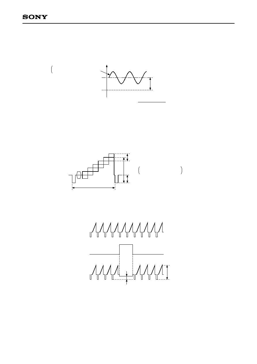
9)
Fab is a frequency response difference between the direct DL and 1/2H DL.
10)
Chroma 40 IRE
140 IRE
40 IRE
1H 63.5Ķs
1.1Vp-p at DG
CCD
2.2Vp-p at DG
in2
or DG
DL
DG is measured with a vectorscope in each mode of the 5-stage waves.
11) Measure S/N of the BPF 100kHz to 4.2MHz in the subcarrier trap mode with a video noise meter.
12)
2Vp-p
V
VD
SIG DELAY
Input waveform
EXT VD input
SIG OUT
Output waveform
Set a voltage value at V
VD
when inserting EXT VD to the 2Vp-p signal output waveform sync tip of SIG OUT.

≠ 9 ≠
CXL1008M/P
3fsc (10.738635MHz) Sine wave
0.15 to 1.0Vp-p
CLOCK
Function Outline
Output signal selection
50mV
REF
SIG OUT
SIG IN2
(PB)
SIG DELAY
(JOG)
The video output signal is selected by selecting the output switch for three signals: Pin 10 (MUTE IN), Pin 17
(JOG IN) and Pin 16 (EXT VD).
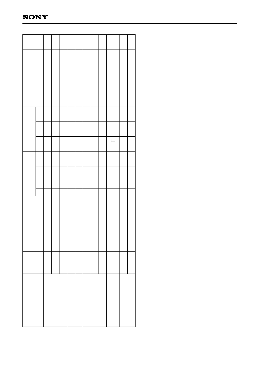
Table 1. Logic Table of Signal Output Selection State
Input control signal state
Video signal output selection state
JOG IN
0
0
0
0
1
1
1
1
0
0
1
1
0
0
1
1
0
1
0
1
0
1
0
1
O
O
◊
◊
◊
◊
◊
◊
◊
◊
◊
◊
O
◊
◊
◊
◊
◊
◊
◊
◊
O
◊
O
◊
◊
O
O
◊
◊
O
O
MUTE IN
EXT VD
PB
JOG
VD insert
MUTE
Note 1) Figures "0" and "1" of the input control signal state are equivalent to "Low" and "High" of logic.
Note 2) Items marked with the symbol "O" in the video signal output selection state are selected.
Note 3) PB = JOG IN ∑ MUTE IN
JOG = JOG IN ∑ MUTE IN ∑ EXT VD
VD insert = JOG IN ∑ EXT VD
MUTE = MUTE IN

≠ 10 ≠
CXL1008M/P
CCD selection
CCD OUT
SIG
IN1
SKEW IN
1/2H (359bit)
D (20bit)
Table 2. Logic Table of CCD DL Mode
Selection
Control signal
SKEW IN
0
1
D
◊
O
1/2H
O
◊
CCD DL mode
Application Circuit
3fsc
0.3Vp-p
SINE WAVE
EXT
VD
JOG
IN
2
3
4
5
6
7
8
9
10
1
11
12
13
14
15
16
17
18
19
20
21
22
23
24
25
26
27
28
0.01ĶF
22Ķ
10k
10Ķ
REC/PB
9V
1k
560
220k
100k
MUTE
IN
5V
10Ķ
2M
0.047Ķ
2M
0.047Ķ
510
SIGNAL
INPUT
510
47Ķ
1000p
Transistor to be used
PNP: 2SA1175
SIGNAL OUTPUT
1.5k
1.8k
120 10ĶH
220p 270p
0.022Ķ
220
8.2k
390
390
4.7k
2.2k
10k
220k
18k
10Ķ
2k
10Ķ
1000p
47Ķ
1M
SKEW IN
Frequency characteristics (Ta = 25įC)
10k
100k
1M
f ≠ Frequency [Hz]
Gain [dB]
≠2
≠1
0
Application circuits shown are typical examples illustrating the operation of the devices. Sony cannot assume responsibility for
any problems arising out of the use of these circuits or for any infringement of third party patent and other right due to same.

≠ 11 ≠
CXL1008M/P
5.00
4.75
V
CL
≠ Supply voltage [V]
Supply voltage (V
CL
) vs.
Insert gain (IG
CCD
)
IG
CCD
≠ Insert gain [dB]
≠2
≠1
0
1
2
≠3
5.25
5.00
4.75
V
CL
≠ Supply voltage [V]
Supply voltage (V
CL
) vs.
Frequency characteristics (f
CCD
)
f
CCD
≠ Frequency characteristics [dB]
≠3
≠2
≠1
0
1
≠4
5.25
5.00
4.75
V
CL
≠ Supply voltage [V]
Supply voltage (V
CL
) vs.
Differential gain (DG
CCD
)
DG
CCD
≠ Differential gain [%]
1
2
3
4
5
0
5.25
5.00
4.75
V
CL
≠ Supply voltage [V]
Supply voltage (V
CL
) vs.
Output pin voltage (V
do
1)
V
do
1 ≠ Output pin voltage [V]
2.0
2.5
1.5
5.25
9.0
8.5
V
DD
≠ Supply voltage [V]
Supply voltage (V
DD
) vs.
Insert gain (IG
CCD
)
IG
CCD
≠ Insert gain [dB]
≠2
≠1
0
1
2
≠3
9.5
9.0
8.5
V
DD
≠ Supply voltage [V]
Supply voltage (V
DD
) vs.
Frequency characteristics (f
CCD
)
f
CCD
≠ Frequency characteristics [dB]
≠3
≠2
≠1
0
1
≠4
9.5

≠ 12 ≠
CXL1008M/P
9.0
8.5
V
DD
≠ Supply voltage [V]
Supply voltage (V
DD
) vs.
Differential gain (DG
CCD
)
DG
CCD
≠ Differential gain [%]
1
2
3
4
5
0
9.5
9.0
8.5
V
DD
≠ Supply voltage [V]
Supply voltage (V
DD
) vs.
Output pin voltage (V
do
1)
V
do
1 ≠ Output pin voltage [V]
2.0
2.5
1.5
9.5
20
0
Ta ≠ Ambient temperature [įC]
Ambient temperature (Ta) vs.
Insert gain (IG
CCD
)
IG
CCD
≠ Insert gain [dB]
≠2
≠1
0
1
2
≠3
60
40
20
0
Ta ≠ Ambient temperature [įC]
Ambient temperature (Ta) vs.
Differential gain (DG
CCD
)
DG
CCD
≠ Differential gain [%]
1
2
3
4
5
0
60
40
20
0
Ta ≠ Ambient temperature [įC]
Ambient temperature (Ta) vs.
Frequency characteristics (f
CCD
)
f
CCD
≠ Frequency characteristics [dB]
≠3
≠2
≠1
0
1
≠4
60
40
20
0
Ta ≠ Ambient temperature [įC]
Ambient temperature (Ta) vs.
Output pin voltage (V
do
1)
V
do
1 ≠ Output pin voltage [V]
2.0
2.5
1.5
60
40
≠ 13 ≠
CXL1008M/P
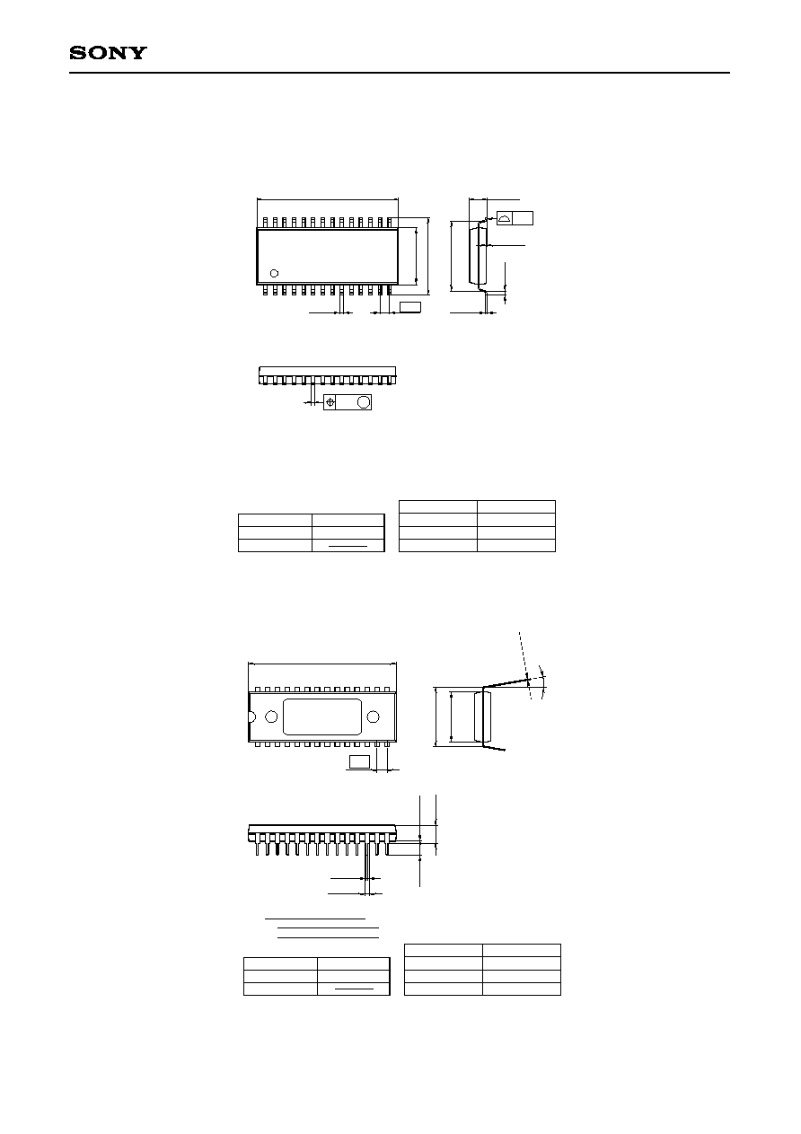
Package Outline
Unit: mm
CXL1008M
28PIN SOP (PLASTIC)
18.8 ≠ 0.1
+ 0.4
0.45 Ī 0.1
1.27
10.3 Ī
0.4
7.6 ≠ 0.1
+ 0.3
0.5 Ī
0.2
0.15 ≠ 0.05
+ 0.1
0.1 ≠ 0.05
+ 0.2
2.3 ≠ 0.15
+ 0.4
M
0.24
SONY CODE
EIAJ CODE
JEDEC CODE
PACKAGE STRUCTURE
PACKAGE MATERIAL
LEAD TREATMENT
LEAD MATERIAL
PACKAGE MASS
EPOXY RESIN
SOLDER PLATING
42/COPPER ALLOY
SOP-28P-L02
SOP028-P-0375
0.6g
9.3
1
14
28
15
0.15
CXL1008P
SONY CODE
EIAJ CODE
JEDEC CODE
PACKAGE STRUCTURE
PACKAGE MATERIAL
LEAD TREATMENT
LEAD MATERIAL
PACKAGE MASS
EPOXY RESIN
SOLDER PLATING
COPPER ALLOY
DIP-28P-03
DIP028-P-0600
4.2g
28PIN DIP (PLASTIC)
37.8 ≠ 0.1
+ 0.4
28
15
1
14
2.54
0.5 Ī 0.1
1.2 Ī 0.15
3.0 MIN
0.5 MIN
4.6 ≠ 0.1
+ 0.4
15.24
13.0 ≠ 0.1
+ 0.3
0.25 ≠ 0.05
+ 0.1
0į to 15į
1.All mat surface type.
Two kinds of package surface:
2.Center part is mirror surface.