
CMOS-CCD Signal Processor
Description
The CXL1501M is a CMOS-CCD signal processor
designed for 8-mm VCR video signal processing. In
combination with the 8-mm VCR video Y/C signal
processing IC CXA1200Q, this IC configures a comb
filter for Y/C separation in recording an image and
elimination of crosstalk in playing back.
Features
∑ Single power supply 5V
∑ Low power consumption 225mW (Typ.)
∑ Built-in peripheral circuits
∑ Completely adjustment free
∑ Built-in quadruple progression PLL circuit
∑ For NTSC signals
Functions
∑ 1H comb filter output
∑ Dropout compensation (D.O.C) output
∑ Delay time matching through output (THR)
∑ PLL circuit (quadruple progression)
∑ Clock driver
∑ Autobias circuit
∑ Sync tip clamp circuit
∑ Sample and hold circuit
Structure
CMOS-CCD
Absolute Maximum Ratings (Ta = 25∞C)
∑ Supply voltage
V
DD
6
V
∑ Operating temperature
Topr
≠10 to +60
∞C
∑ Storage temperature
Tstg ≠55 to +150 ∞C
∑ Allowable power dissipation P
D
500
mW
Recommended Operating Conditions (Ta = 25∞C)
Supply voltage
V
DD
5
±
5%
V
Recommended Clock Conditions (Ta = 25∞C)
∑ Input clock amplitude
V
CLK
0.4 to 1.0 Vp-p
(0.5Vp-p Typ.)
∑ Clock frequency
f
CLK
3.579545 MHz
∑ Input clock waveform
sine wave
Input Signal Amplitude
V
SIG
571 mVp-p
(Max.)
≠ 1 ≠
E71050-PS
Sony reserves the right to change products and specifications without prior notice. This information does not convey any license by
any implication or otherwise under any patents or other right. Application circuits shown, if any, are typical examples illustrating the
operation of the devices. Sony cannot assume responsibility for any problems arising out of the use of these circuits.
CXL1501M
30 pin SOP (Plastic)
For the availability of this product, please contact the sales office.
≠ 2 ≠
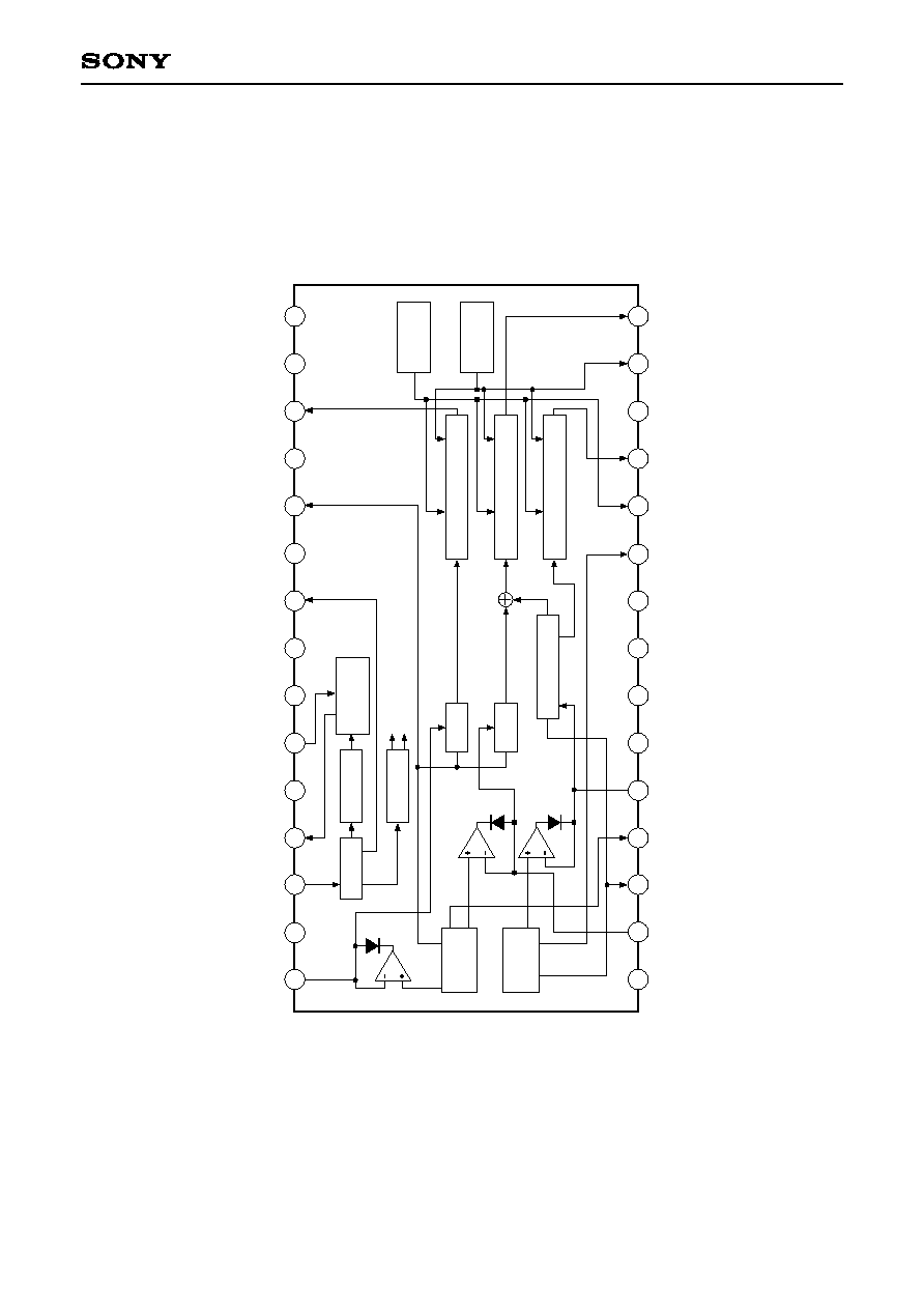
CXL1501M
Block Diagram and Pin Configuration (Top View)
2
3
6
7
8
9
10
11
12
13
14
15
16
17
18
19
20
21
22
23
24
26
27
28
29
30
1
Phase
comparator
1
2
V
SS
CCD2
ADJC
ABN
CCD3
NC
V
DD
V
SS
NC
ABP
VGGA
YD
V
SS
VGGB
Y-YD
CCD1
V
SS
VCO IN
PC OUT
V
DD
CLK
V
SS
NC
VCO OUT
NC
ADJY
V
DD
TH
V
SS
V
SS
D
IH + D
D
Bias circuit
(A)
Bias circuit
(B)
VCO
1/4 divider
Clock driver
Autobias
circuit (N)
Autobias
circuit (P)
4
25
Output circuit, S/H circuit
Output circuit, S/H circuit
Output circuit, S/H circuit
5
≠ 3 ≠
CXL1501M
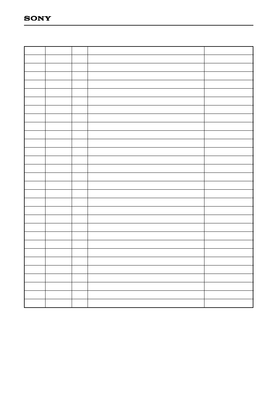
Pin Description
Pin No.
Symbol
I/O
Description
1
2
3
4
5
6
7
8
9
10
11
12
13
14
15
16
17
18
19
20
21
22
23
24
25
26
27
28
29
30
V
SS
CCD2
ADJC
ABN
CCD3
NC
V
DD
V
SS
NC
ABP
VGGA
YD
V
SS
VGGB
Y-YD
V
SS
V
SS
TH
V
DD
ADJY
NC
VCO OUT
NC
V
SS
CLK
V
DD
PC OUT
VCO IN
V
SS
CCD1
--
I
O
O
I
--
--
--
--
O
O
O
--
O
O
--
--
O
--
O
--
O
--
--
I
--
O
I
--
I
GND
Signal input 2 (Reverse phase signal)
Forward phase CCD bias DC output
Reverse phase autobias DC output
Signal input 3 (Forward phase signal)
5V power supply (For clock driver)
GND
Forward phase autobias DC output
Gate bias (A) DC output
D.O.C signal output (Reverse phase signal)
GND
Gate bias (B) DC output
Comb filter signal output
GND
GND
THR signal output (Forward phase signal)
5V power supply (For analog)
Reverse phase CCD bias DC output
VCO output
GND
Clock input
5V power supply (For digital)
Phase comparator output
VCO input
GND
Signal input 1 (Reverse phase signal)
Impedance (
)
> 100k (at no clamp)
600 to 2k
2k to 20k
> 100k (at no clamp)
2k to 20k
2k to 10k
40 to 500
2k to 10k
40 to 500
40 to 500
600 to 2k
4k to 40k
2k to 5k
> 100k
> 100k (at no clamp)

