 | –≠–ª–µ–∫—Ç—Ä–æ–Ω–Ω—ã–π –∫–æ–º–ø–æ–Ω–µ–Ω—Ç: CXL1505M | –°–∫–∞—á–∞—Ç—å:  PDF PDF  ZIP ZIP |

CMOS-CCD Signal Processor
Description
CXL1503M/1505M are CMOS-CCD signal processors
developed for CCD camera complementary color filter
array processing system.
CXL1503M 1H
◊
4 301.5 bit CCD delay line
CXL1505M 1H
◊
4 453.5 bit CCD delay line
Features
∑ Single power supply 5V
∑ Low power consumption
CXL1503M 100mW (Typ.)
CXL1505M 150mW (Typ.)
∑ Built-in peripheral circuits
∑ Built-in CDS (Correlated Double Sampling) circuit
Function
∑ Clock driver
∑ Autobias circuit (center and black)
∑ Pedestal clamp circuit
∑ CDS circuit
Structure
CMOS-CCD
Absolute Maximum Ratings (Ta = 25∞C)
∑ Supply voltage
V
DD
6
V
∑ Operating temperature
Topr
≠10 to +60
∞C
∑ Storage temperature
Tstg ≠55 to +150 ∞C
∑ Allowable power dissipation P
D
500
mW
Recommended Operating Conditions (Ta = 25∞C)
Supply voltage
V
DD
5
±
5%
V
Recommended Clock Conditions (Ta = 25∞C)
≠ 1 ≠
E89174A03-PS
Sony reserves the right to change products and specifications without prior notice. This information does not convey any license by
any implication or otherwise under any patents or other right. Application circuits shown, if any, are typical examples illustrating the
operation of the devices. Sony cannot assume responsibility for any problems arising out of the use of these circuits.
CXL1503M/1505M
24 pin SOP (Plastic)
Item
Clock voltage Low
Clock voltage High
Clock frequency
Symbol
V
L
V
H
f
CL
f
CL
CXL1503M
CXL1505M
Min.
0
V
DD
≠ 1.0
Typ.
4.77
7.16
Unit
V
V
MHz
MHz
Remarks
NTSC: 910f
H
/3
CCIR: 908f
H
/3
NTSC: 455f
H
CCIR: 454f
H
Max.
1.0
V
DD

≠ 2 ≠
CXL1503M/1505M
2
3
4
5
6
7
8
9
10
11
12
13
14
15
16
17
18
19
20
21
22
23
24
1
DL A
TIMING GENERATOR
A. B
CENTER
A. B
BLACK
DL B
DL C
DL D
P. D
P. D
PG GEN.
PG GEN.
PG GEN.
PG GEN.
CLP
CLP
CLP
CLP
WAVE
FORM
INPUT
SOURCE
POTENTIAL
CONTROL
CDS-OUTPUT
CIRCUIT
CDS-OUTPUT
CIRCUIT
CDS-OUTPUT
CIRCUIT
CDS-OUTPUT
CIRCUIT
BIAS.
OUT D
OUT C
OUT B
OUT A
V
SS
V
DD
V
SS
V
SS
V
DD
V
DD
XDL2
XDL1
ABCN
ABBL
DCAB
IN A
IN B
IN C
IN D
CLP
IS
N.C.
V
GG
CDS
5V
2
3
4
5
6
7
8
9
10
11
12
13
14
15
16
17
18
19
20
21
22
23
24
1
V
SS
IN C
ABBL
V
DD
IS
IN D
CLP
V
DD
OUT D
V
GG
OUT C
N.C.
IN B
DCAB
IN A
ABCN
V
DD
XDL1
XDL2
V
SS
V
SS
OUT A
CDS
OUT B
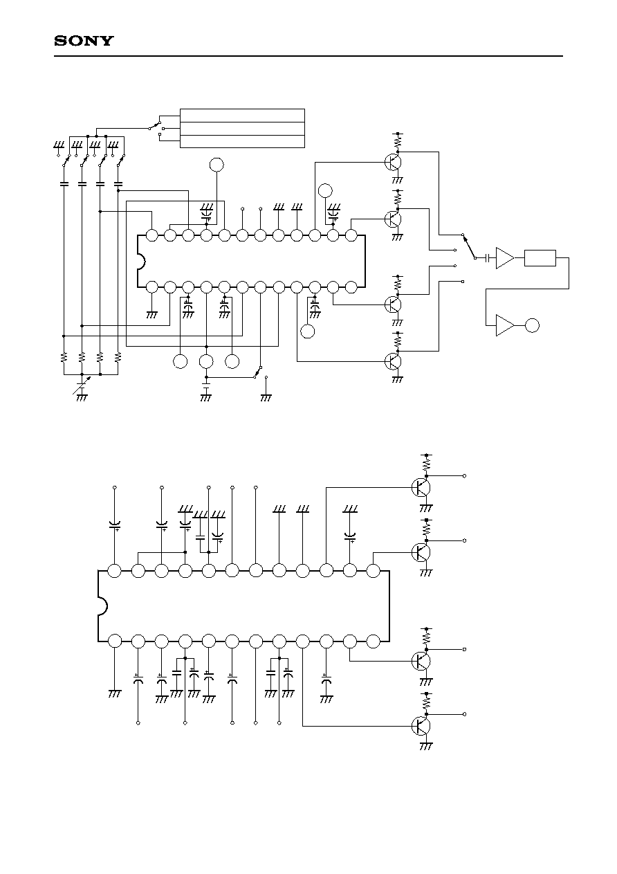
Pin Description
No.
Symbol
I/O
Description
1, 16, 17
2
3
4, 8, 20
5
6
7
9
10
11
12
13
14
15
18
19
21
22
23
24
V
SS
IN C
ABBL
V
DD
IS
IN D
CLP
OUT D
V
GG
OUT C
N.C.
OUT B
CDS
OUT A
XDL2
XDL1
ABCN
IN A
DCAB
IN B
--
I
O
--
O
I
I
O
O
O
--
O
O
O
I
I
O
I
I
I
GND
Signal input C channel
Autobias DC output for Y signal
5V power supply
Input source DC output
Signal input D channel
Clamp pulse input
Signal output D channel
Gate bias DC output
Signal output C channel
--
Signal output B channel
DC output for CDS
Signal output A channel
Clock pulse input 2
Clock pulse input 1
Autobias DC output for C signal
Signal input A channel
DC bias input for A and B channel
Signal input B channel
Pin Configuration (Top View)
Impedance (
)
> 100k (at no clamp)
2k to 20k
5k
> 100k (at no clamp)
> 100k
50 to 500
2k to 10k
50 to 500
50 to 500
500 to 5k
50 to 500
> 100k
> 100k
2k to 20k
> 100k (at no clamp)
> 100k
> 100k (at no clamp)
Block Diagram

≠ 3 ≠
CXL1503M/1505M
Item
Autobias center level
Autobias black level
Input source level
CDS source level
Output circuit bias level
Supply
1
current
Insertion gain
Frequency
1
response
Linearity
Insertion gain difference
between channels
Linearity
difference
between
channels
Cross talk
between channels
ABCN
ABBL
IS
CDS
V
GG
I
DD
IG
f
G
Lin.
G
L
AB
L
CD
CRT
V
1
V
2
V
3
V
4
V
5
A
1
V
6
V
6
V
6
V
6
Symbol
Test
Point
SW position
SW1
a
a
a
a
a
b
b
c
b
a
b
b
a
a
a
a
b
b
b
b
a
a
a
a
a
a
a to d
a to d
a to d
a to d
a
a
a
a
a
a
a
a
a
a
b
SW2
SW3
SW4 to 7
Bias condition
Conditions
Min.
1.0
1.2
0.3
1.2
0.3
--
--
≠4.5
≠1.8
≠1.5
0
0
0
0
0
2.0
2.2
0.6
2.3
0.8
20
30
≠3.5
≠0.8
≠0.4
5
5
1
1
1
4.0
4.2
3.0
3.5
3.0
35
40
≠0.5
--
--
12
15
5
5
3
V
V
V
V
V
mA
dB
dB
%
%
%
%
%
Typ.
Max.
Unit
E1
V
1
A, Bch
V
1
C, Dch
V
2
≠ 0.2V
A, Bch
V
1
C, Dch
V
2
≠ 0.2V
CXL1503M
CXL1505M
CXL1503M
CXL1505M
Ach
Bch
Cch
Dch
Output amplitude (mVp-p)
20 log
Input amplitude (SIN 100kHz, 100mVp-p)
Output amplitude (SIN 1MHz, 100mVp-p)
20 log
Output amplitude (SIN 100kHz, 100mVp-p)
(Note 1)
(Note 2)
(Note 3)
(Note 3)
(Note 4)
1
Standerd values are different between CXL1503M and CXL1505M.
Electrical Characteristics
(Ta = 25∞C, V
DD
= 5.0V, V
SS
= 0V)
f
CL
= 4.77MHz (CXL1503M)
f
CL
= 7.16MHz (CXL1505M)

≠ 4 ≠
CXL1503M/1505M
Notes)
1. Linearity testing
For A channel and B channel, set input bias E
1
to ABCN + 0.2 [V] first, and then set it to ABCN [V] and ABCN
≠ 0.2 [V]. Then input a sine wave of 100kHz and 100mVp-p, and compare the three output amplitudes.
For C channel and D channel, set input bias E
1
to ABBL ≠ 0.4 [V] first, and then set it to ABBL ≠ 0.2 [V] and
ABBL [V]. Then input a sine wave of 100kHz and 100mVp-p, and compare the three output amplitudes.
The maximum output amplitude for the respective A, B, C and D channels is taken as Sout max. and the
minimum output amplitude as Sout min. The linearity of the respective channels is defined as
Sout max ≠ Sout min
Lin =
◊
200 [%]
Sout max + Sout min
2. Calculation of insertion gain difference
As the max. insertion gain among A, B, C and D channels' is taken as Gmax and the min. as Gmin., the
insertion gain difference between channels becomes:
G = ABS (1 ≠ 10 )
◊
100 [%]
3. Calculation of linearity difference
Define A channel linearity as L
A
, and B channel linearity as L
B
. We obtain the difference
L
AB
as follows.
L
AB
=
L
A
≠ L
B
[%]
Similarly we obtain the linearity difference
L
CD
of C channel and D channel as follows.
L
CD
=
L
C
≠ L
D
[%]
4. Crosstalk calculation
We take CRTa as: A channel crosstalk value only during B channel input
CRTb as: B channel crosstalk value only during A channel input
CRTc as: C channel crosstalk value only during D channel input
CRTd as: D channel crosstalk value only during C channel input
The crosstalk value of respective channels becomes:
Crosstalk component
CRTa to d =
◊
100 [%]
Each channel output value
Gmax ≠ Gmin
(
20
)

≠ 5 ≠
CXL1503M/1505M
Clock Waveform Timing
10ns
10ns
10%
50%
90%
XDL
1
(52.5)
87.5ns
(140)
210ns
10%
50%
90%
10ns
10%
50%
90%
(52.5)
87.5ns
10%
50%
90%
10ns
17.5ns
XDL
2
( ) is for CXL1505M.
≠ 6 ≠
CXL1503M/1505M
Electrical Characteristics Test Circuit
10k 10k 10k
10k
V4
V5
V3
V2
A1
V1
a
SW4
a
a
a
b
b
b
b
SW5
SW6
SW7
No signal
100kHz, 100mVp-p sine wave
1MHz, 100mVp-p sine wave
a
b
c
SW1
5V
3.3k
5V
3.3k
5V
3.3k
5V
3.3k
◊
1
◊
1
LPF
V6
b
a
d
c
SW3
1µ
16V
2
3
4
5
6
7
9
10
11
12
13
14
15
16
17
18
19
21
22
23
24
1
a
b
E1
V
DD
5V
1µ
16V
1µ
16V
1µ
16V
(NC)
1µ
16V
XDL1 XDL2
20
8
SW2
Application Circuit
5V
3.3k
5V
3.3k
5V
3.3k
5V
3.3k
1µ
16V
1µ
16V
(NC)
4.7µ
16V
100p
4.7µ
16V
100p
1µ
16V
0.1µ
16V
0.1µ
16V
0.1µ
16V
1µ
16V
4.7µ
16V
100p
1µ
16V
0.1µ
16V
Output A
V
DD
Input
B
Input
A
XDL
1
XDL
2
Output B
Output C
Output D
V
DD
Input
C
Input
D
CLP
Input
V
DD
2
3
4
5
6
7
8
9
10
11
12
1
13
14
15
16
17
18
19
20
21
22
23
24
Application circuits shown are typical examples illustrating the operation of the devices. Sony cannot assume responsibility for
any problems arising out of the use of these circuits or for any infringement of third party patent and other right due to same.
≠ 7 ≠
CXL1503M/1505M
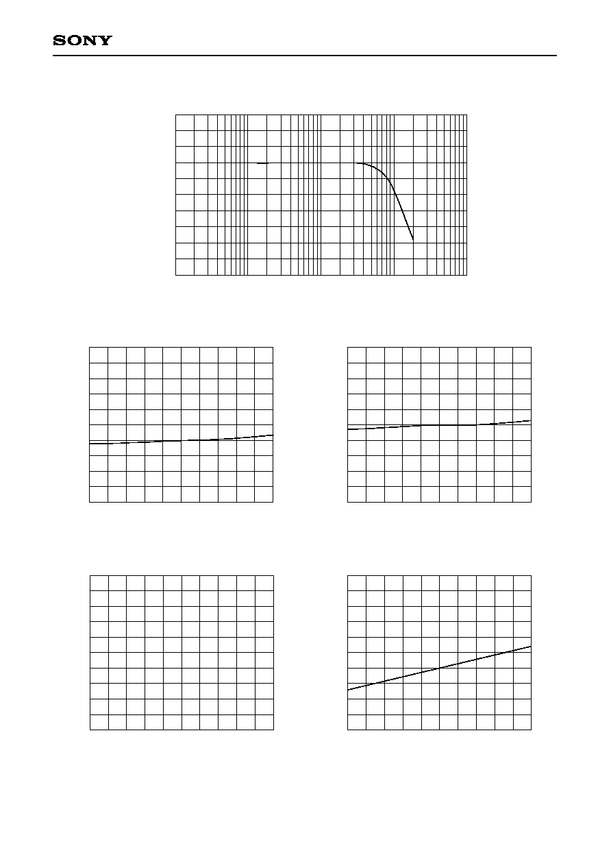
Signal frequency [Hz]
≠2
≠3
≠4
≠5
≠6
≠7
Insertion gain [dB]
10k
100k
1M
10M
Frequency response
3
2
1
ABCN ≠ Autobias center level [V]
V
DD
≠ Supply voltage [V]
5
5.5
Autobias center level vs. Supply voltage
4.5
3
2
1
ABBL ≠ Autobias black level [V]
V
DD
≠ Supply voltage [V]
5
5.5
Autobias black level vs. Supply voltage
4.5
0
≠2.5
≠5
IG ≠ Insertion gain [dB]
V
DD
≠ Supply voltage [V]
5
5.5
Insertion gain vs. Supply voltage
4.5
10
5
0
Lin ≠ Linearity [%]
V
DD
≠ Supply voltage [V]
5
5.5
Linearity vs. Supply voltage
4.5

≠ 8 ≠
CXL1503M/1505M
fG ≠ Frequency response [dB]
V
DD
≠ Supply voltage [V]
5
5.5
4.5
3
2
Ta ≠ Ambient temperature [∞C]
3
2
1
Ta ≠ Ambient temperature [∞C]
Ta ≠ Ambient temperature [∞C]
Insertion gain vs. Ambient temperature
60
10
5
0
Lin ≠ Linearity [%]
Ta ≠ Ambient temperature [∞C]
0
Linearity vs. Ambient temperature
20
40
60
fG ≠ Frequency response [dB]
Ta ≠ Ambient temperature [∞C]
20
40
60
Frequency response vs. Ambient temperature
Autobias black level vs. Ambient temperature
Autobias center level vs. Ambient temperature
Frequency response vs. Supply voltage
ABBL ≠ Autobias black level [V]
IG ≠ Insertion gain [dB]
ABCN ≠ Autobias center level [V]
0
20
40
0
60
20
40
0
1
0
≠1
≠2
60
20
40
0
0
≠2.5
≠5
0
≠1
≠2
≠ 9 ≠
CXL1503M/1505M
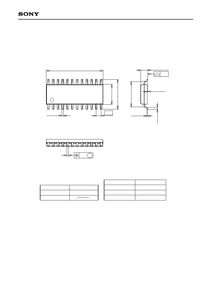
Package Outline
Unit: mm
SONY CODE
EIAJ CODE
JEDEC CODE
M
PACKAGE STRUCTURE
MOLDING COMPOUND
LEAD TREATMENT
LEAD MATERIAL
PACKAGE MASS
EPOXY RESIN
SOLDER PLATING
42/COPPER ALLOY
24PIN SOP (PLASTIC)
15.0 ≠ 0.1
+ 0.4
1
12
13
24
0.45 ± 0.1
5.3 ≠ 0.1
+ 0.3
7.9 ±
0.4
0.2 ≠ 0.05
+ 0.1
0.5 ±
0.2
0.1 ≠ 0.05
+ 0.2
0.15
1.85 ≠ 0.15
+ 0.4
6.9
0.24
SOP-24P-L01
SOP024-P-0300
0.3g
1.27