 | –≠–ª–µ–∫—Ç—Ä–æ–Ω–Ω—ã–π –∫–æ–º–ø–æ–Ω–µ–Ω—Ç: CXL5502M | –°–∫–∞—á–∞—Ç—å:  PDF PDF  ZIP ZIP |
CMOS-CCD 1H Delay Line for NTSC
Description
The CXL5502M/N/P are CMOS-CCD delay line ICs
that provide 1H delay time for NTSC signals including
the external low-pass filter.
The ICs contain a PLL circuit (quadruple progression).
Features
∑ Single power supply (5V)
∑ Low power consumption 95mW (Typ.)
∑ Built-in peripheral circuits
∑ Clamp level of I/O signal can be selected
∑ Built-in quadruple PLL circuit
Functions
∑ 905-bit CCD register
∑ Clock driver
∑ Autobias circuit
∑ Input clamp circuit
∑ Sample and hold circuit
∑ PLL circuit (quadruple progression)
Structure
CMOS-CCD
Absolute Maximum Ratings (Ta = 25∞C)
∑ Supply voltage
V
DD
6
V
∑ Operating temperature Topr
≠10 to +60
∞C
∑ Storage temperature
Tstg
≠55 to +150
∞C
∑ Allowable power dissipation
P
D
CXL5502M
400
mW
CXL5502N
260
mW
CXL5502P
800
mW
Recommended Operating Condition (Ta = 25∞C)
Supply voltage
V
DD
5 ± 5%
V
Recommended Clock Conditions (Ta = 25∞C)
∑ Input clock amplitude
V
CLK
0.3 to 1.0
Vp-p
(0.5Vp-p typ.)
∑ Clock frequency
f
CLK
3.579545
MHz
∑ Input clock waveform
Sine wave
Input Signal Amplitude
V
SIG
500mVp-p (Typ.), 572mVp-p (Max.)
(at internal clamp condition)
≠ 1 ≠
E89930E79-PS
Sony reserves the right to change products and specifications without prior notice. This information does not convey any license by
any implication or otherwise under any patents or other right. Application circuits shown, if any, are typical examples illustrating the
operation of the devices. Sony cannot assume responsibility for any problems arising out of the use of these circuits.
CXL5502M/N/P
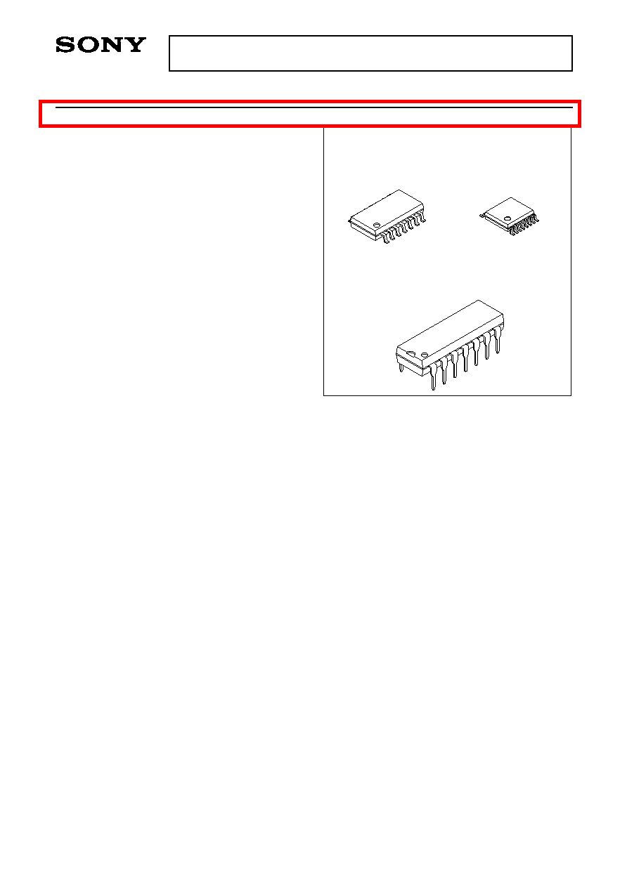
CXL5502M
14 pin SOP (Plastic)
CXL5502N
16 pin SSOP (Plastic)
CXL5502P
14 pin DIP (Plastic)
For the availability of this product, please contact the sales office.

≠ 2 ≠
CXL5502M/N/P
Autobias circuit
Clock driver
Bias circuit (A)
Bias circuit (B)
PLL
Timing circuit
CCD
(905bit)
Clamp circuit
Output circuit
(S/H 1bit)
14
V
SS
12
V
DD
11
VCO
IN
10
PC
OUT
9
V
DD
8
CLK
1
IN
2
I/O1
3
I/O2
4
OUT
5
V
SS
7
VCO
OUT
6
V
SS
I/O control
13
AB
14
V
DD
12
PC
OUT
11
(N.C)
10
V
DD
9
CLK
8
VCO
OUT
1
IN
2
I/O1
3
I/O2
4
OUT
5
V
SS
7
V
SS
6
(N.C)
13
VCO
OUT
15
AB
16
V
SS
Block Diagram and Pin Configuration (Top View)
CXL5502M/P
CXL5502N
Autobias circuit
Clock driver
Bias circuit (A)
Bias circuit (B)
PLL
Timing circuit
CCD
(905bit)
Clamp circuit
Output circuit
(S/H 1bit)
I/O control

≠ 3 ≠
CXL5502M/N/P
Pin Description
CXL5502M/P
CXL5502N
Pin No.
Symbol
I/O
Description
Impedance
1
2
3
4
5
6
7
8
9
10
11
12
13
14
IN
I/O1
I/O2
OUT
V
SS
V
SS
VCO OUT
CLK
V
DD
PC OUT
VCO IN
V
DD
AB
V
SS
I
I
I
O
--
--
O
I
--
O
I
--
O
--
Signal input
I/O control 1
I/O control 2
Signal output
GND
GND
VCO output
Clock input
Power supply (5V)
Phase comparator output
VCO input
Power supply (5V)
Autobias DC output
GND (SUB)
> 10k
at no clamp
40 to 500
> 100k
600 to 200k
Pin No.
Symbol
I/O
Description
Impedance
1
2
3
4
5
6
7
8
9
10
11
12
13
14
15
16
IN
I/O1
I/O2
OUT
V
SS
(N.C)
V
SS
VCO OUT
CLK
V
DD
(N.C)
PC OUT
VCO IN
V
DD
AB
V
SS
I
I
I
O
--
--
--
O
I
--
--
O
I
--
O
--
Signal input
I/O contorl 1
I/O contorl 2
Signal output
GND
--
GND
VCO output
Clock input
Power supply (5V)
--
Phase comparator output
VCO input
Power supply (5V)
Autobias DC output
GND (SUB)
> 10k
at no clamp
40 to 500
> 100k
600 to 200k

≠ 4 ≠
CXL5502M/N/P
Description of Function
In the CXL5502M/N/P, the condition of I/O control pins (Pins 2 and 3) control the input signal clamp condition
and the mode of the output signal with relation to its input signal.
There are 2 modes for the I/O signal.
(1) PN mode
(Low level clamp/reverse phase output mode)
(2) NP mode
(High level clamp/positive phase output mode)
I/O Control Pin
(1) I/O1 (Pin 2)
Control of the I/O signal condition
DC open .....
Input signal is low level clamped and the output signal is inverted in relation to the input
signal. As the pin is biased to 2.5V by means of the resistance inside the IC, a decoupling
capacitor of around 1000pF is necessary.
GND ............. Input signal is high level clamped and the output signal turns into an inverted signal.
(2) I/O2 (Pin 3)
Control of the input signal clamp condition
0V ................. Internal clamp condition
5V ................. Non internal clamp condition
Center biased to approx. 2.1V by means of the IC internal resistance (several 10k
).
Usage in this mode is limited to APL 50% signals and in this mode, the maximum input
signal amplitude is 200mVp-p.
Clamp
level
Input waveform
Output waveform
Clamp
level
≠ 5 ≠
CXL5502M/N/P
--
--
2.1
--
--
VINPN + 0.5
VINNP
--
b
a
b
a
b
a
b
a
b
a
b
a
b
a
b
a
b
a
b
a
b
a
b
a
b
a
b
a
10
≠2
≠2
0
0
--
52
19
0
≠1
5
5
--
56
28
2
0
7
7
350
--
mA
dB
dB
%
degree
mVp-p
dB
2
3
4
5
5
6
7
Unit
Note
Max.
Min.
Typ.
Bias condition
Vbias1 (V)
(Note 1)
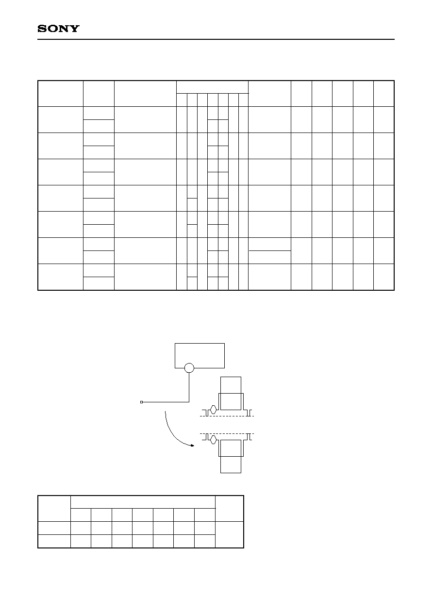
Electrical Characteristics
(Ta = 25∞C, V
DD
= 5V, f
CLK
= 3.579545MHz, V
CLK
= 500mVp-p, Sine wave)
See "Electrical Characteristics Test Circuit"
Notes
(1) VINPN and VINNP are defined as follows.
VINPN and VINNP are the input signal clamp levels of PN and NP modes clamping the video signal sync
tip level.
Testing of VINPN and VINNP is executed with a voltmeter under the following SW conditions.
Item
Symbol
Test condition
SW condition
1 2 3 4 5 6 7
--
a
b
c
d
d
--
e
c
a
a
a
b
a
b
c
a
b
b
b
a
b
b
a
b
a
a
b
a
a
b
a
--
b
b
c
c
a
d
--
200kHz,
500mVp-p,
sine wave
200kHz
3.57MHz,
150mVp-p,
sine wave
5-staircase wave
(See Note 5)
5-staircase wave
(See Note 5)
No signal input
50% white
video signal
(See Note 7)
IDDPN
IDDNP
GLPN
GLNP
fPN
fNP
DGPN
DGNP
DPPN
DPNP
CPPN
CPNP
SNPN
SNNP
Supply
current
Low
frequency
gain
Frequency
response
Differential
gain
Differential
phase
S/H pulse
coupling
S/N ratio
1
Input
(IN)
VINPN
CXL5502
VINNP
SW condition
Item
VINPN
VINNP
Test
point
V1
1
--
--
2
c
c
3
b
b
4
b
a
5
b
a
6
a
a
7
--
--
≠ 6 ≠
CXL5502M/N/P
(2) This is the IC supply current value during clock and signal input.
(3) GLPN, GLNP are output gain of OUT pin when a 500mVp-p, 200kHz sine wave is fed to IN pin.
(Example of calculation)
GLPN = 20 log [dB]
(4) Indicates the dissipation at 3.57MHz in relation to 200kHz.
From the output voltage at OUT pin when a 150mVp-p, 200kHz sine wave is fed to IN pin, and from the
output voltage at OUT pin when a 150mVp-p, 3.57MHz sine wave is fed to same, calculation is made
according to the following formula. The input part bias is tested at 2.1V.
(Example of calculation)
fPN = 20 log [dB]
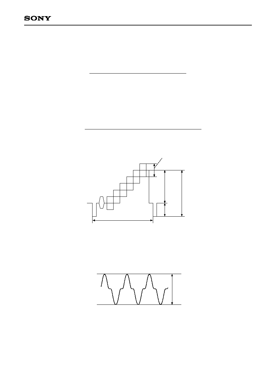
(5) The differential gain (DG) and the differential phase (DP), when the 5-staircase wave in the figure below is
input are tested at the vector scope.
Input waveform (Input waveform of NP mode is the inverted waveform in the figure above)
(6) The internal clock component to the output signal during no-signal input and the leakage of that high
harmonic component are tested. The input part bias is tested at VINPN + 0.5V and VINNP for PN and NP
modes respectively.
OUT pin output voltage (PN mode) [mVp-p]
500 [mVp-p]
OUT pin otuput voltage (PN mode, 3.57MHz) [mVp-p]
OUT pin output voltage (PN mode, 200kHz) [mVp-p]
1H 63.56µs
143mV
357mV
500mV
143mV
Test value
(mVp-p)

≠ 7 ≠
CXL5502M/N/P
(7) S/N ratio during a 50% white video signal input shown in figure below is tested at a video noise meter, in
BPF 100kHz to 4MHz, Sub Carrier Trap mode.
Input waveform (Input waveform of NP mode is the inverted waveform in the figure above)
Clock
1H 63.56µs
143mV
178mV
321mV
0.3Vp-p to 1.0Vp-p
(0.5Vp-p typ.)
fsc (3.579545MHz) sine wave

≠ 8 ≠
CXL5502M/N/P
Electrical Characteristics Test Circuit
(Using CXL5502M/P)
V
S
S
A
B
V
D
D
V
C
O
I
N
P
C
O
U
T
V
D
D
C
L
K
1
0
0
0
P
1
0
0
0
P
3
.
3
µ
3
.
3
µ
0
.
1
µ
1
k
8
2
k
0
.
1
µ
1
µ
C
L
K
f
S
C
(
3
.
5
7
9
5
4
5
M
H
z
)
0
.
5
V
p
-
p
s
i
n
e
w
a
v
e
I
N
I
/
O
1
I
/
O
2
O
U
T
V
S
S
V
C
O
O
U
T
V
S
S
a
b
S
W
6
a
b
1
M
1
k
A
V
1
5
V
c
1
0
0
0
P
1
µ
S
W
2
b
S
W
1
c
2
0
0
k
H
z
5
0
0
m
V
p
-
p
s
i
n
e
w
a
v
e
2
0
0
k
H
z
1
5
0
m
V
p
-
p
s
i
n
e
w
a
v
e
3
.
5
7
M
H
z
1
5
0
m
V
p
-
p
s
i
n
e
w
a
v
e
5
-
s
t
a
i
r
c
a
s
e
w
a
v
e
5
0
%
w
h
i
t
e
v
i
d
e
o
s
i
g
n
a
l
a
b
d
e
a
S
W
7
2
.
1
k
9
V
2
3
4
5
6
7
1
b
c
d
O
s
c
i
l
l
o
s
c
o
p
e
S
p
e
c
t
r
u
m
a
n
a
l
y
z
e
r
V
e
c
t
o
r
s
c
o
p
e
N
o
i
s
e
m
e
t
e
r
N
o
t
e
1
)
N
o
t
e
2
)
◊
3
◊
3
L
P
F
B
P
F
N
o
t
e
1
)
L
P
F
f
r
e
q
u
e
n
c
y
r
e
s
p
o
n
s
e
0
≠
3
≠
5
0
6
M
1
4
.
3
M
[
H
z
]
F
r
e
q
u
e
n
c
y
[
d
B
]
N
o
t
e
2
)
B
P
F
f
r
e
q
u
e
n
c
y
r
e
s
p
o
n
s
e
0
≠
3
≠
5
0
6
M
1
4
.
3
M
[
H
z
]
F
r
e
q
u
e
n
c
y
[
d
B
]
2
0
0
8
9
1
0
1
1
1
2
1
3
1
4
S
W
3
V
b
i
a
s
1
C
X
L
5
5
0
2
M
/
P
a
1
≠
1
1
0
0
0
P
a
b
a
b
S
W
4
S
W
5
When using CXL5502N, change the connection terminal only.
(See the block diagram and pin configuration. For NC pins, ground them.)

≠ 9 ≠
CXL5502M/N/P
Application Circuit
(Using CXL5502M/P)
1
0
0
0
P
3
.
3
µ
1
k
3
.
3
µ
0
.
1
µ
8
2
k
1
0
0
0
P
0
.
1
µ
1
µ
f
S
C
0
.
5
V
p
-
p
s
i
n
e
w
a
v
e
1
M
1
µ
3
3
p
3
3
0
k
8
9
1
0
1
1
1
2
1
3
1
4
5
V
2
3
4
5
6
7
1
I
n
p
u
t
4
7
0
2
7
0
0
5
6
0
k
1
k
L
P
F
2
7
p
2
2
0
0
2
2
0
0
5
V
2
2
0
0
1
µ
O
u
t
p
u
t
T
r
a
n
s
i
s
t
o
r
u
s
e
d
P
N
P
:
2
S
A
1
1
7
5
T
r
a
n
s
i
s
t
o
r
u
s
e
d
N
P
N
:
2
S
C
4
0
3
D
e
l
a
y
t
i
m
e
2
5
0
n
s
(
e
x
.
T
H
3
5
6
L
S
M
-
4
3
0
3
Z
E
D
T
o
u
k
o
u
m
a
d
e
)
(
P
o
s
i
t
i
v
e
p
h
a
s
e
s
i
g
n
a
l
)
(
P
o
s
i
t
i
v
e
p
h
a
s
e
s
i
g
n
a
l
)
(
R
e
v
e
r
s
e
p
h
a
s
e
s
i
g
n
a
l
)
1
0
0
0
P
7
1
.
8
k
4
f
S
C
2
S
C
4
0
3
1
.
8
k
5
V
V
C
O
O
U
T
(
P
i
n
7
)
i
n
u
s
e
C
X
L
5
5
0
2
M
/
P
When using CXL5502N, change the connection terminal only.
(See the block diagram and pin configuration. For NC pins, ground them.)
Application circuits shown are typical examples illustrating the operation of the devices. Sony cannot assume responsibility fo
r
any problems arising out of the use of these circuits or for any infringement of third party patent and other right due to same
.

≠ 10 ≠
CXL5502M/N/P
Example of Representative Characteristics
Low frequency gain vs. Ambient temperature
≠20
0
20
40
60
80
≠3
≠2
≠1
0
1
Ambient temperature [∞C]
L
o
w
f
r
e
q
u
e
n
c
y
g
a
i
n
[
d
B
]
Differential gain vs. Ambient temperature
≠20
0
20
40
60
80
2
4
6
8
10
0
Ambient temperature [∞C]
D
i
f
f
e
r
e
n
t
i
a
l
g
a
i
n
[
%
]
Low frequency gain vs. Supply voltage
4.75
5
5.25
≠3
≠2
≠1
0
1
Supply voltage [V]
L
o
w
f
r
e
q
u
e
n
c
y
g
a
i
n
[
d
B
]
Supply current vs. Ambient temperature
≠20
0
20
40
60
80
10
30
20
Ambient temperature [∞C]
S
u
p
p
l
y
c
u
r
r
e
n
t
[
m
A
]
Frequency response vs. Ambient temperature
≠20
0
20
40
60
80
≠2
≠1
0
≠3
Ambient temperature [∞C]
F
r
e
q
u
e
n
c
y
r
e
s
p
o
n
s
e
[
d
B
]
Supply current vs. Supply voltage
4.75
5
5.25
10
30
20
Supply voltage [V]
S
u
p
p
l
y
c
u
r
r
e
n
t
[
m
A
]

≠ 11 ≠
CXL5502M/N/P
Differential gain vs. Supply voltage
4.75
5
5.25
2
4
6
8
10
0
Supply voltage [V]
D
i
f
f
e
r
e
n
t
i
a
l
g
a
i
n
[
%
]
Frequency response vs. Supply voltage
4.75
5
5.25
≠2
≠1
0
≠3
Supply voltage [V]
F
r
e
q
u
e
n
c
y
r
e
s
p
o
n
s
e
[
d
B
]
Frequency response
10k
100k
1M
≠6
≠4
≠2
0
2
Frequency [Hz]
G
a
i
n
[
d
B
]
10M

≠ 12 ≠
CXL5502M/N/P
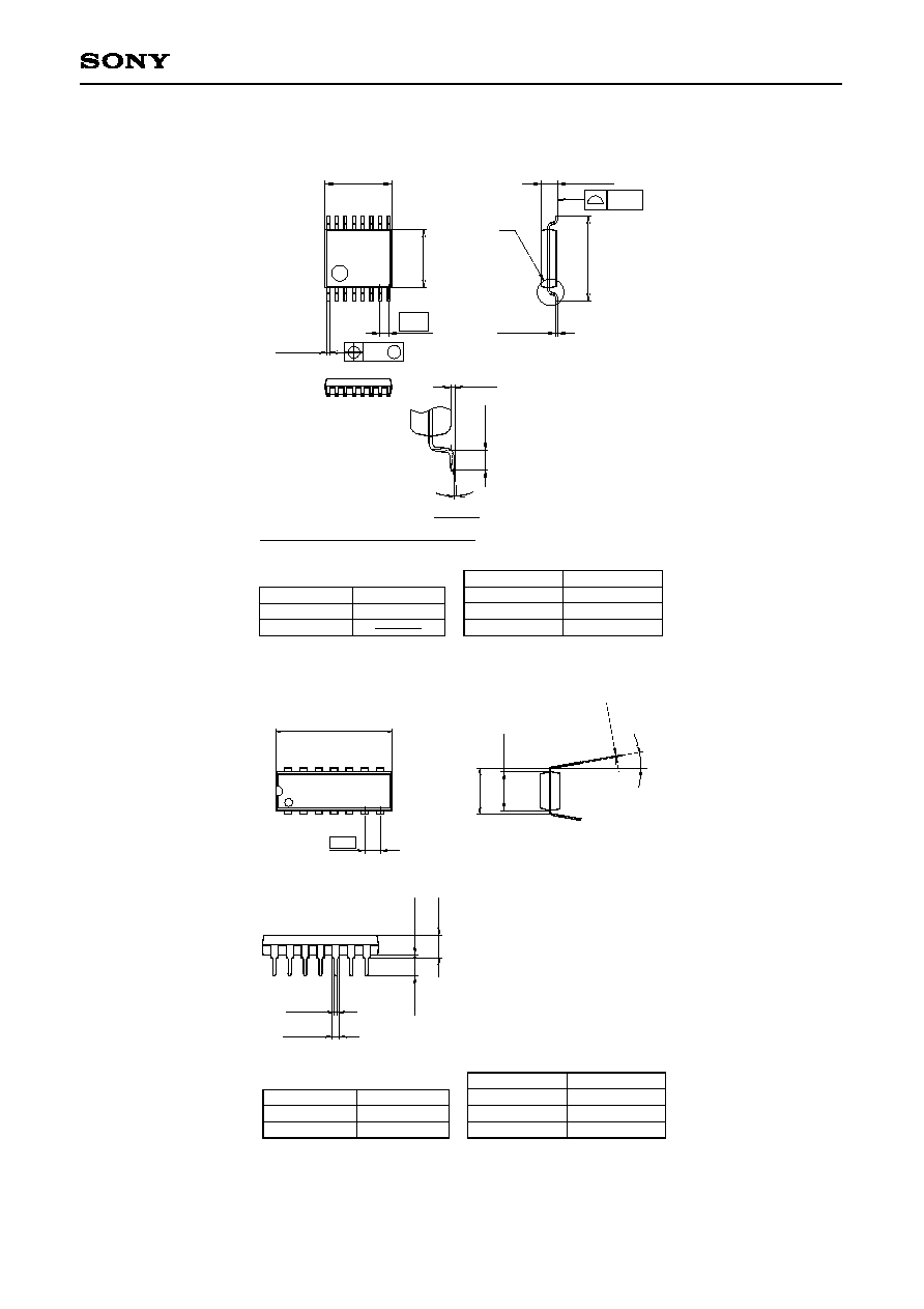
Package Outline
Unit: mm
CXL5502M
14PIN SOP (PLASTIC)
9.9 ≠ 0.1
+ 0.4
0.45 ± 0.1
1.27
7
.
9
±
0
.
4
5
.
3
≠
0
.
1
+
0
.
3
6
.
9
0
.
5
±
0
.
2
0.2 ≠ 0.05
+ 0.1
0.1 ≠ 0.05
+ 0.2
1.85 ≠ 0.15
+ 0.4
M
0.24
SONY CODE
EIAJ CODE
JEDEC CODE
PACKAGE STRUCTURE
PACKAGE MATERIAL
LEAD TREATMENT
LEAD MATERIAL
PACKAGE MASS
EPOXY RESIN
SOLDER PLATING
42/COPPER ALLOY
SOP-14P-L01
SOP014-P-0300
0.2g
1
7
14
8
0.15
14PIN SOP (Plastic) 300mil
2
0
M
A
X
1.27
5
.
3
±
0
.
3
10.2 ± 0.3
0.15
0.15 ± 0.0
5
10∞ MAX
SONY CODE
EIAJ CODE
JEDEC CODE
PACKAGE STRUCTURE
PACKAGE MATERIAL
LEAD TREATMENT
LEAD MATERIAL
PACKAGE WEIGHT
EPOXY RESIN
SOLDER PLATING
COPPER / 42 ALLOY
SOP-14P-L121
SOP014-P-0300-AX
14
8
0.4 ± 0.1
1.44 MAX
7
.
8
±
0
.
4
1
7
A
0
.
7
5
±
0
.
2
0.05 MIN
DETAIL A
M
0.13
0.2g
≠ 13 ≠
CXL5502M/N/P
16PIN SSOP (PLASTIC)
SONY CODE
EIAJ CODE
JEDEC CODE
PACKAGE STRUCTURE
PACKAGE MATERIAL
LEAD TREATMENT
LEAD MATERIAL
PACKAGE MASS
EPOXY RESIN
SOLDER / PALLADIUM
42/COPPER ALLOY
0.1g
SSOP-16P-L01
SSOP016-P-0044
5.0 ± 0.1
0.65
0.22 ≠ 0.05
+ 0.1
8
1
9
16
4
.
4
±
0
.
1
6
.
4
±
0
.
2
0.1 ± 0.1
0
.
5
±
0
.
2
0∞ to 10∞
0.15 ≠ 0.02
+ 0.05
1.25 ≠ 0.1
+ 0.2
A
DETAIL A
0.1
PLATING
NOTE: Dimension "
" does not include mold protrusion.
0.13 M
14PIN DIP (PLASTIC)
19.2 ≠ 0.1
+ 0.4
1
2.54
7
8
14
6
.
4
≠
0
.
1
+
0
.
3
0
.
2
5
≠
0
.
0
5
+
0
.
1
7
.
6
2
0∞ to 15∞
3
.
7
≠
0
.
1
+
0
.
4
0
.
5
M
I
N
0.5 ± 0.1
3
.
0
M
I
N
1.2 ± 0.15
SONY CODE
EIAJ CODE
JEDEC CODE
DIP-14P-01
DIP014-P-0300
Similar to MO-001-AH
PACKAGE STRUCTURE
PACKAGE MATERIAL
LEAD TREATMENT
LEAD MATERIAL
PACKAGE MASS
EPOXY RESIN
SOLDER PLATING
42/COPPER ALLOY
0.9g
CXL5502P
CXL5502N