 | –≠–ª–µ–∫—Ç—Ä–æ–Ω–Ω—ã–π –∫–æ–º–ø–æ–Ω–µ–Ω—Ç: CXL5509M | –°–∫–∞—á–∞—Ç—å:  PDF PDF  ZIP ZIP |

CMOS-CCD 1H/2H Delay Line for NTSC
Description
The CXL5509M/P is a CMOS-CCD delay line
developed for video signal processing. Usage in
conjunction with an external low-pass filter provide 1H
and 2H delay signals simultaneously (For NTSC
signals).
Features
∑ Single power supply (5V)
∑ Low power consumption 130mW (Typ.)
∑ Built-in peripheral circuits
∑ Built-in quadruple PLL circuit
∑ For NTSC signals
∑ 1 input and 2 outputs
(Outputs for both 1H and 2H delays)
Functions
∑ 906-bit (1H) and 1816-bit (2H) CCD register
∑ Clock driver
∑ Auto-bias circuit
∑ Sync tip clamp circuit
∑ Sample-and-hold circuit
∑ Quadruple PLL circuit
Structure
CMOS-CCD
Absolute Maximum Ratings (Ta = 25∞C)
∑ Supply voltage
V
DD
6
V
∑ Operating temperature Topr
≠10 to +60
∞C
∑ Storage temperature
Tstg
≠55 to +150
∞C
∑ Allowable power dissipation
P
D
CXL5509M
400
mW
CXL5509P
800
mW
Recommended Operating Condition (Ta = 25∞C)
Supply voltage
V
DD
5 ± 5%
V
Recommended Clock Conditions (Ta = 25∞C)
∑ Input clock amplitude
V
CLK
0.3 to 1.0
Vp-p
(0.5Vp-p typ.)
∑ Clock frequency
f
CLK
3.579545
MHz
∑ Input clock waveform
sine wave
Input Signal Amplitude
V
SIG
571mVp-p (Max.) (at internal clamp condition)
≠ 1 ≠
E91401B7X-PS
Sony reserves the right to change products and specifications without prior notice. This information does not convey any license by
any implication or otherwise under any patents or other right. Application circuits shown, if any, are typical examples illustrating the
operation of the devices. Sony cannot assume responsibility for any problems arising out of the use of these circuits.
CXL5509M/P
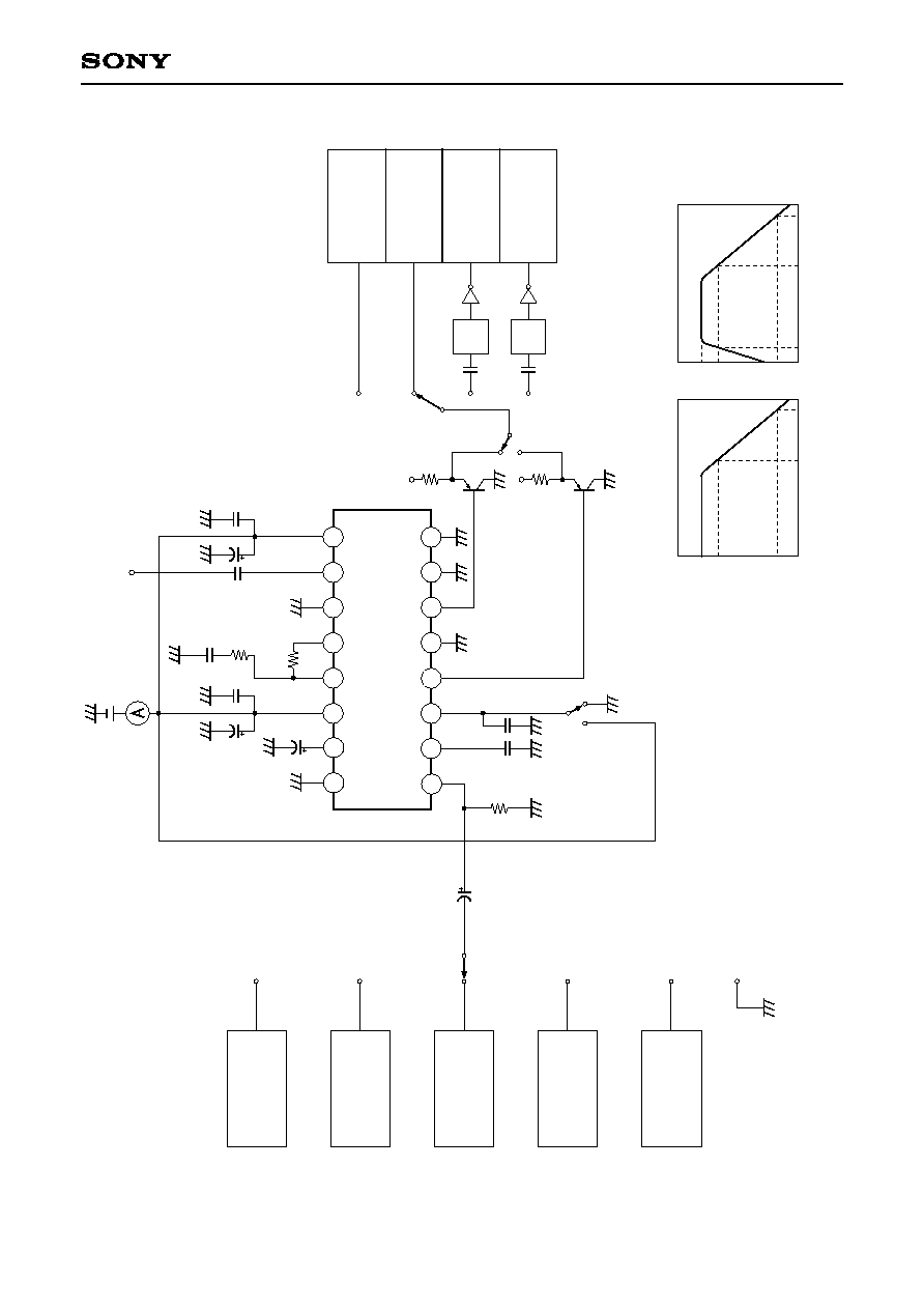
Blook Diagram and Pin Configuration (Top View)
Output circuit
(S/H 1bit)
CLK
1
2
3
4
5
7
Auto-bias circuit
Timing circuit
CCD
(1816bit)
Driver
Bias circuit
Clamp circuit
6
VCO IN
V
DD
AB
OUT1 (1H)
VG2
VG1
IN
9
10
11
12
13
14
V
SS
V
SS
V
SS
(VCO OUT)
V
SS
V
SS
PC OUT
PLL
15
16
Output circuit
(S/H 1bit)
8
V
DD
906bit
1816bit
OUT2 (2H)
CXL5509M
16 pin SOP (Plastic)
CXL5509P
16 pin DIP (Plastic)
≠ 2 ≠
CXL5509M/P
Pin Description
Pin No.
Symbol
Description
Impedance
I/O
1
2
3
4
5
6
7
8
9
10
11
12
13
14
15
16
IN
VG1
VG2
OUT1
V
SS
OUT2
V
SS
(VCO OUT)
V
SS
V
DD
CLK
V
SS
PC OUT
VCO IN
V
DD
AB
V
SS
I
O
I
O
--
O
(O)
--
--
I
--
O
I
--
O
--
Signal input
(Non-inverted signal)
Gate bias 1 DC output
Gate bias 2 DC input
1H signal output
(Inverted signal)
GND
2H signal output
(Inverted signal)
GND or VCO output (4fsc)
GND
Power supply (5V)
Clock input (fsc)
GND
Phase comparator output
VCO input
Power supply (5V)
Autobias DC output
GND
> 10k
(at no clamp)
40 to 500
40 to 500
> 10k
600 to 200k
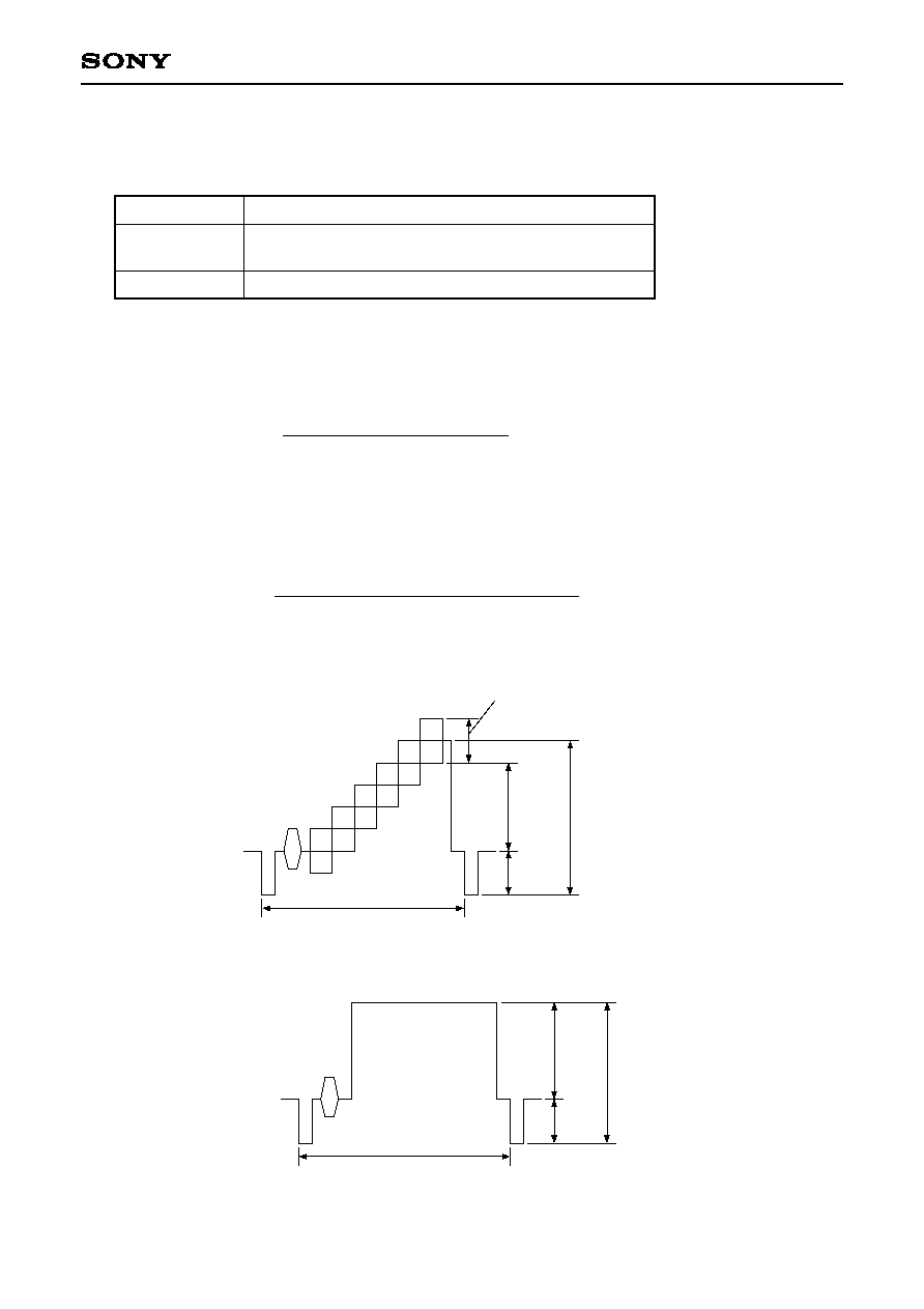
Description of Pin 3 (VG2)
Control of input signal clamp condition
0V ........ Sync tip clamp condition
5V ........ Center bias condition
The input signal is biased to approx. 2.1V by means of the IC internal resistance (approx. 10k
).
In this mode, the input signal is limited to APL 50% and the maximum input signal amplitude is at
200mVp-p.
≠ 3 ≠
CXL5509M/P
b
b
b
a
a
b
b
b
b
b
b
b
b
a
a
b
a
b
a
b
a
b
a
b
a
b
16
≠2
≠2
≠2.0
≠2.0
--
--
--
--
52
52
--
--
26
0
0
≠1.0
≠1.0
3
3
3
3
56
56
--
--
36
2
2
0
0
5
5
5
5
--
--
350
350
mA
dB
dB
%
degree
dB
mVp-p
2
3
4
5
5
6
7
Unit
Note
Max.
Min. Typ.
Electrical Characteristics
(Ta = 25∞C, V
DD
= 5V, f
CLK
= 3.579545MHz, V
CLK
= 500mVp-p, sine wave)
See "Electrical Characteristics Test Circuit"
Item
Symbol
Test conditions
(Note 1)
SW conditions
1
2
3
4
a
a
a
b
c
b
c
d
d
d
d
e
e
f
f
a
b
b
b
b
c
c
c
c
d
d
a
a
--
200kHz,
500mVp-p,
sine wave
200kHz
3.58MHz,
150mVp-p,
sine wave
5-staircase wave
5-staircase wave
50% white
video signal
No signal input
I
DD
GL1
GL2
fR1
fR2
DG1
DG2
DP1
DP2
SN1
SN2
CP1
CP2
Supply current
Low frequency
gain
Frequency
response
Differential
gain
Differential
phase
S/N ratio
S/H pulse coupling
Electrical Characteristics Test Circuit
10
00
p
1
µ
A
B
V
D
D
V
C
O
I
N
C
L
K
1
0
0
0
p
8
2
k
3
.
3
µ
0
.
1
µ
C
L
K
f
S
C
(
3
.
5
7
9
5
4
5
M
H
z
)
,
5
0
0
m
V
p
-
p
s
i
n
e
w
a
v
e
I
N
V
G
2
O
U
T
1
V
S
S
a
b
1
M
5
V
1
µ
S
W
1
c
a
b
d
e
a
S
W
4
b
c
d
◊
3
◊
3
L
P
F
B
P
F
0
≠
3
≠
5
0
6
M
1
4
.
3
M
[
d
B
]
6
M
1
4
.
3
M
2
0
0
10
00
p
0
≠
3
≠
5
0
[
d
B
]
f
1
2
3
4
5
7
8
6
9
1
0
1
1
1
2
1
3
1
4
V
S
S
P
C
O
U
T
V
S
S
V
S
S
V
G
1
V
S
S
(
V
C
O
O
U
T
)
1
0
0
0
p
3
.
3
µ
0
.
1
µ
1
2
0
1
5
1
6
V
D
D
O
U
T
2
C
X
L
5
5
0
9
M
/
P
S
W
2
S
W
3
a
b
0
0
2
0
0
k
H
z
5
0
0
m
V
p
-
p
s
i
n
e
w
a
v
e
2
0
0
k
H
z
1
5
0
m
V
p
-
p
s
i
n
e
w
a
v
e
3
.
5
8
M
H
z
1
5
0
m
V
p
-
p
s
i
n
e
w
a
v
e
5
-
s
t
a
i
r
c
a
s
e
w
a
v
e
5
0
%
w
h
i
t
e
v
i
d
e
o
s
i
g
n
a
l
O
s
c
i
l
l
o
s
c
o
p
e
S
p
e
c
t
r
u
m
a
n
a
l
y
z
e
r
V
e
c
t
o
r
s
c
o
p
e
N
o
i
s
e
m
e
t
e
r
N
o
t
e
1
)
N
o
t
e
2
)
N
o
t
e
1
)
L
P
F
f
r
e
q
u
e
n
c
y
r
e
s
p
o
n
s
e
F
r
e
q
u
e
n
c
y
[
H
z
]
N
o
t
e
2
)
B
P
F
f
r
e
q
u
e
n
c
y
r
e
s
p
o
n
s
e
F
r
e
q
u
e
n
c
y
[
H
z
]
≠ 4 ≠
CXL5509M/P
≠ 5 ≠
CXL5509M/P
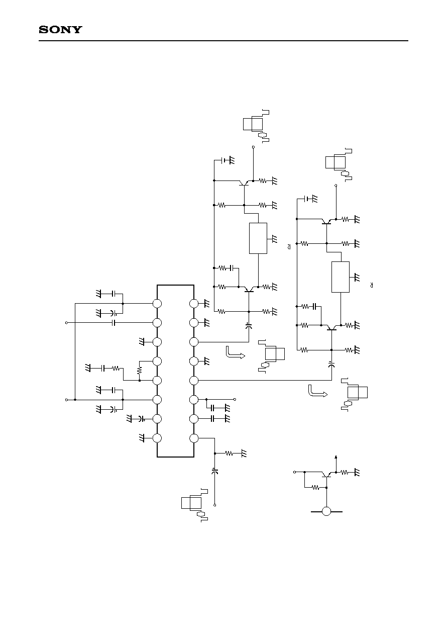
Application Circuit
1
0
0
0
p
1
0
0
0
p
3
.
3
µ
0
.
1
µ
1
µ
C
L
K
f
S
C
(
3
.
5
7
9
5
4
5
M
H
z
)
,
5
0
0
m
V
p
-
p
s
i
n
e
w
a
v
e
1
M
1
µ
3
3
0
k
5
V
S
i
g
n
a
l
i
n
p
u
t
(
N
o
n
-
i
n
v
e
r
t
e
d
s
i
g
n
a
l
)
5
1
0
5
6
0
k
1
k
L
P
F
2
.
2
k
2
.
2
k
5
V
2
.
2
k
1
µ
T
r
a
n
s
i
s
t
o
r
u
s
e
d
P
N
P
:
2
S
A
1
1
7
5
T
r
a
n
s
i
s
t
o
r
u
s
e
d
N
P
N
:
2
S
C
4
0
3
D
e
l
a
y
t
i
m
e
1
7
0
n
s
(
N
o
n
-
i
n
v
e
r
t
e
d
s
i
g
n
a
l
)
(
I
n
v
e
r
t
e
d
s
i
g
n
a
l
)
1
2
3
4
5
7
6
8
9
1
0
1
1
1
2
1
3
1
4
1
0
0
0
p
3
.
3
µ
0
.
1
µ
8
2
k
1
2
0
1
.
8
k
7
1
.
8
k
5
V
4
f
S
C
O
U
T
N
o
t
e
)
W
h
e
n
V
C
O
O
U
T
(
P
i
n
7
)
i
s
u
s
e
d
t
h
e
c
i
r
c
u
i
t
b
e
l
o
w
.
W
h
e
n
n
o
t
u
s
e
d
,
G
N
D
.
1
5
1
6
1
0
0
0
p
1
k
3
0
p
3
3
0
k
5
1
0
5
6
0
k
1
k
L
P
F
2
.
2
k
2
.
2
k
5
V
2
.
2
k
1
µ
1
H
O
u
t
p
u
t
T
r
a
n
s
i
s
t
o
r
u
s
e
d
P
N
P
:
2
S
A
1
1
7
5
T
r
a
n
s
i
s
t
o
r
u
s
e
d
N
P
N
:
2
S
C
4
0
3
D
e
l
a
y
t
i
m
e
1
7
0
n
s
(
N
o
n
-
i
n
v
e
r
t
e
d
s
i
g
n
a
l
)
(
I
n
v
e
r
t
e
d
s
i
g
n
a
l
)
1
k
3
0
p
T
r
a
n
s
i
s
t
o
r
u
s
e
d
N
P
N
:
2
S
C
4
0
3
V
1
2
H
O
u
t
p
u
t
Application circuits shown are typical examples illustrating the operation of the devices. Sony cannot assume responsibility fo
r
any problems arising out of the use of these circuits or for any infringement of third party patent and other right due to same
.
≠ 6 ≠
CXL5509M/P
Notes
(1) By switching SW2, input condition turns out as follows.
(2) This is the IC supply current value during clock and signal input.
(3) GL is the output gain of OUT pin when a 500mVp-p, 200kHz sine wave is fed to IN pin.
GL = 20 log [dB]
(4) Indicates the dissipation at 3.58MHz in relation to 200kHz.
From the output voltage at OUT pin when a 150mVp-p, 200kHz sine wave is fed to IN pin, and from the
output voltage at OUT pin when a 150mVp-p, 3.58MHz sine wave is fed to same, calculation is made
according to the following formula.
fR = 20 log [dB]
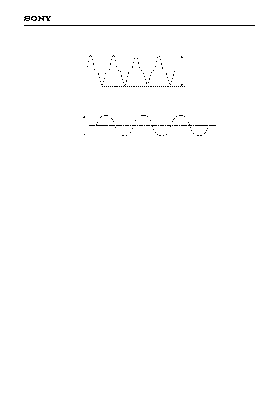
(5) The differential gain (DG) and the differential phase (DP), when the 5-staircase wave in the following
figure is fed, are tested with a vector scope:
OUT pin output voltage [mVp-p]
500 [mVp-p]
OUT pin otuput voltage (3.58MHz) [mVp-p]
OUT pin output voltage (200kHz) [mVp-p]
1H 63.56µs
143mV
285.5mV
500mV
143mV
SW2 condition
a
b
Input condition
Center bias condition (approx. 2.1V)
Approx. 2.1V bias is applied internally to the input signal
Sync tip clamp conditions
(6) S/N ratio during 50% white video signal input shown in figure below is tested at video noise meter, in BPF
100kHz to 4MHz, Sub Carrier Trap mode.
1H 63.56µs
143mV
178mV
321mV
≠ 7 ≠
CXL5509M/P
500mVp-p
(Typ.)
fsc (3.579545MHz) sine wave
Clock
(7) The internal clock component to the output signal during no-signal input and the leakage of that high
harmonic component are tested.
Test value (mVp-p)
≠ 8 ≠
CXL5509M/P
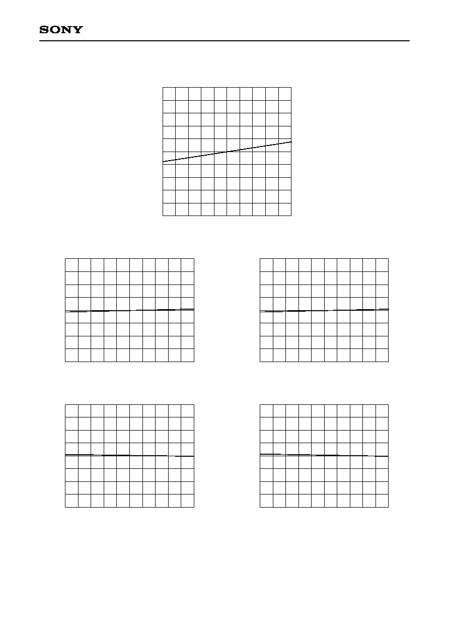
Example of Representative Characteristics
4.75
Supply voltage [V]
Supply current vs. Supply voltage
S
u
p
p
l
y
c
u
r
r
e
n
t
[
m
A
]
26
36
16
5.25
5.0
Low frequency gain (2H) vs. Supply voltage
L
o
w
f
r
e
q
u
e
n
c
y
g
a
i
n
(
2
H
)
[
d
B
]
0
2
≠2
≠1
1
4.75
Supply voltage [V]
5.25
5.0
Low frequency gain (1H) vs. Supply voltage
L
o
w
f
r
e
q
u
e
n
c
y
g
a
i
n
(
1
H
)
[
d
B
]
0
2
≠2
≠1
1
4.75
Supply voltage [V]
5.25
5.0
Frequency response (1H) vs. Supply voltage
F
r
e
q
u
e
n
c
y
r
e
s
p
o
n
s
e
(
1
H
)
[
d
B
]
≠1
1
≠3
≠2
0
4.75
Supply voltage [V]
5.25
5.0
Frequency response (2H) vs. Supply voltage
4.75
Supply voltage [V]
5.25
5.0
F
r
e
q
u
e
n
c
y
r
e
s
p
o
n
s
e
(
2
H
)
[
d
B
]
≠1
1
≠3
≠2
0

≠ 9 ≠
CXL5509M/P
Differential gain (1H) vs. Supply voltage
D
i
f
f
e
r
e
n
t
i
a
l
g
a
i
n
(
1
H
)
[
%
]
3
5
1
2
4
4.75
Supply voltage [V]
5.25
5.0
Differential gain (2H) vs. Supply voltage
D
i
f
f
e
r
e
n
t
i
a
l
g
a
i
n
(
2
H
)
[
%
]
3
5
1
2
4
4.75
Supply voltage [V]
5.25
5.0
0
≠20
Ambient temperature [∞C]
Supply current vs. Ambient temperature
S
u
p
p
l
y
c
u
r
r
e
n
t
[
m
A
]
26
36
16
80
20
40
60
Low frequency gain (2H) vs. Ambient temperature
L
o
w
f
r
e
q
u
e
n
c
y
g
a
i
n
(
2
H
)
[
d
B
]
0
2
≠2
≠1
1
0
≠20
Ambient temperature [∞C]
80
20
40
60
Low frequency gain (1H) vs. Ambient temperature
L
o
w
f
r
e
q
u
e
n
c
y
g
a
i
n
(
1
H
)
[
d
B
]
0
2
≠2
≠1
1
0
≠20
Ambient temperature [∞C]
80
20
40
60

≠ 10 ≠
CXL5509M/P
Frequency response (1H) vs. Ambient temperature
F
r
e
q
u
e
n
c
y
r
e
s
p
o
n
s
e
(
1
H
)
[
d
B
]
≠1
1
≠3
≠2
0
0
≠20
Ambient temperature [∞C]
80
20
40
60
Frequency response (2H) vs. Ambient temperature
F
r
e
q
u
e
n
c
y
r
e
s
p
o
n
s
e
(
2
H
)
[
d
B
]
≠1
1
≠3
≠2
0
0
≠20
Ambient temperature [∞C]
80
20
40
60
Differential gain (2H) vs. Ambient temperature
D
i
f
f
e
r
e
n
t
i
a
l
g
a
i
n
(
2
H
)
[
%
]
4
8
0
2
6
0
≠20
Ambient temperature [∞C]
80
20
40
60
Differential gain (1H) vs. Ambient temperature
D
i
f
f
e
r
e
n
t
i
a
l
g
a
i
n
(
1
H
)
[
%
]
4
8
0
2
6
0
≠20
Ambient temperature [∞C]
80
20
40
60
≠ 11 ≠
CXL5509M/P
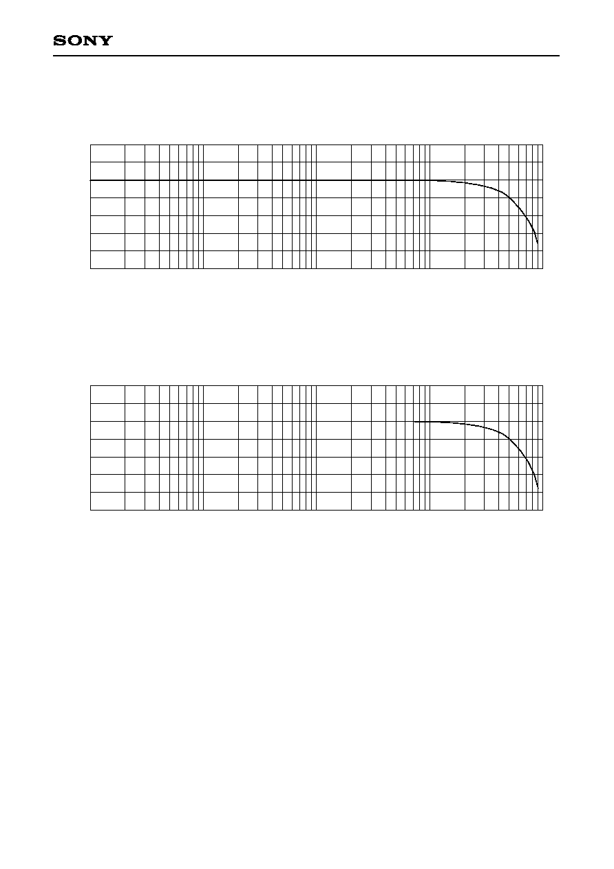
Frequency responses (1H)
Frequency [Hz]
G
i
a
n
[
d
B
]
≠4
2
≠6
0
≠2
10k
1M
100k
10M
Frequency responses (2H)
Frequency [Hz]
G
i
a
n
[
d
B
]
≠4
2
≠6
0
≠2
10k
1M
100k
10M
Note) 1H means 1H output; 2H means 2H output.

≠ 12 ≠
CXL5509M/P
Package Outline
Unit: mm
PACKAGE STRUCTURE
PACKAGE MATERIAL
LEAD TREATMENT
LEAD MATERIAL
PACKAGE MASS
SONY CODE
EIAJ CODE
JEDEC CODE
SOP-16P-L01
SOP016-P-0300
COPPER ALLOY
SOLDER PLATING
EPOXY RESIN
16PIN SOP (PLASTIC)
9.9 ≠ 0.1
+ 0.4
16
9
1
8
1.27
0.45 ± 0.1
5
.
3
≠
0
.
1
+
0
.
3
7
.
9
±
0
.
4
6
.
9
1.85 ≠ 0.15
+ 0.4
0
.
5
±
0
.
2
0.2 ≠ 0.05
+ 0.1
0.1 ≠ 0.05
+ 0.2
0.2g
0.15
M
0.24
PACKAGE STRUCTURE
PACKAGE MATERIAL
LEAD TREATMENT
LEAD MATERIAL
PACKAGE MASS
EPOXY RESIN
SOLDER PLATING
COPPER ALLOY
19.2 ≠ 0.1
+ 0.4
9
1
8
2.54
0.5 ± 0.1
1.2 ± 0.15
3
.
0
M
I
N
0
.
5
M
I
N
3
.
7
≠
0
.
1
+
0
.
4
6
.
4
≠
0
.
1
+
0
.
3
7
.
6
2
0
.
2
5
≠
0
.
0
5
+
0
.
1
0∞ to 15∞
16
16PIN DIP (PLASTIC)
1.0 g
SONY CODE
EIAJ CODE
JEDEC CODE
DIP-16P-01
DIP016-P-0300
Similar to MO-001-AE
1.All mat surface type.
Two kinds of package surface:
2.All mirror surface type.
CXL5509M
CXL5509P