CMOS 8-bit Single Chip Microcomputer
Description
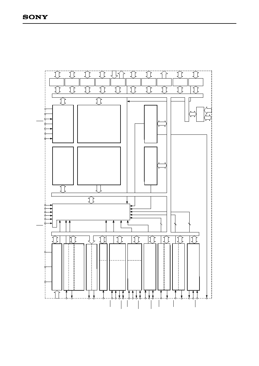
The CXP740056/740096/740010 is a CMOS 8-bit
microcomputer integrating on a single chip an A/D
converter, serial interface, timer/counter, time-base
timer, capture timer/counter, remote control receive
circuit, PWM output, and the like besides the basic
configurations of 8-bit CPU, ROM, RAM, and I/O
port.
The CXP740056/740096/740010 also provides the
sleep/stop functions that enables lower power
consumption.
Features
∑ A wide instruction set (211 instructions) which covers various types of data.
-- 16-bit arithmetic/multiplication and division/Boolean bit operation instructions
∑ Minimum instruction cycle
167ns at 24MHz operation (4.5 to 5.5V)
333ns at 12MHz operation (2.7 to 5.5V)
122µs at 32kHz operation (2.7 to 5.5V)
∑ Incorporated ROM capacity
56K bytes (CXP740056)
96K bytes (CXP740096)
120K bytes (CXP740010)
∑ Incorporated RAM capacity
4096 bytes
∑ Peripheral functions
-- A/D converter
8 bits, 8 channels, successive approximation method
(Conversion time 10.3µs at 24MHz)
-- Serial interface
Srart-stop synchronization (UART), 1 channel
Incorporated buffer RAM (Auto transfer for 1 to 32 bytes), 2 channels
8-bit clock syncronization (MSB/LSB first selectable), 1 channel
-- Timer
8-bit timer 2 channels, 8-bit timer/counter 2 channels,
19-bit time-base timer, 16-bit capture timer/counter
32kHz timer/counter
-- Remote control receive circuit
Noise elimination circuit
8-bit pulse measuring counter, 6-stage FIFO
-- PWM output
12 bits, 2 channels
∑ Interruption
22 factors, 15 vectors, multi-interruption possible
∑ Standby mode
Sleep/stop
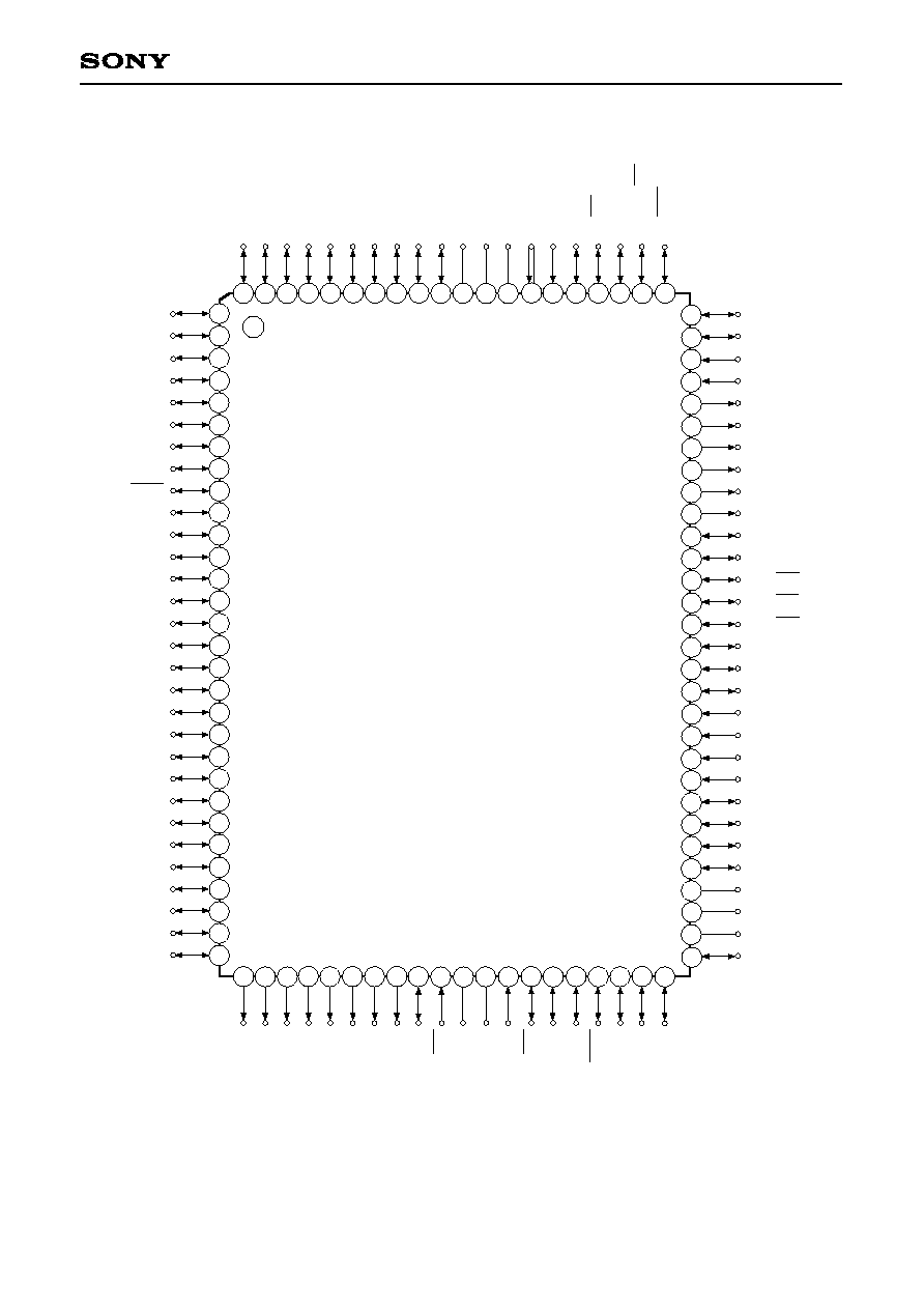
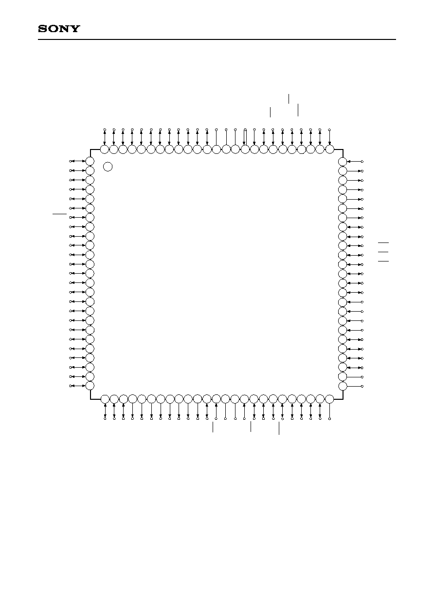
∑ Package
100-pin plastic QFP/LQFP
∑ Piggy/evaluation chip
CXP740000
≠ 1 ≠
E98406-PS
Sony reserves the right to change products and specifications without prior notice. This information does not convey any license by
any implication or otherwise under any patents or other right. Application circuits shown, if any, are typical examples illustrating the
operation of the devices. Sony cannot assume responsibility for any problems arising out of the use of these circuits.
CXP740056/740096/740010
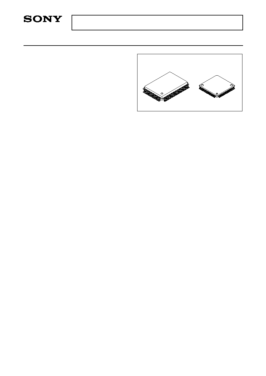
100 pin QFP (Plastic)
100 pin LQFP (Plastic)
Structure
Silicon gate CMOS IC
≠ 5 ≠
CXP740056/740096/740010
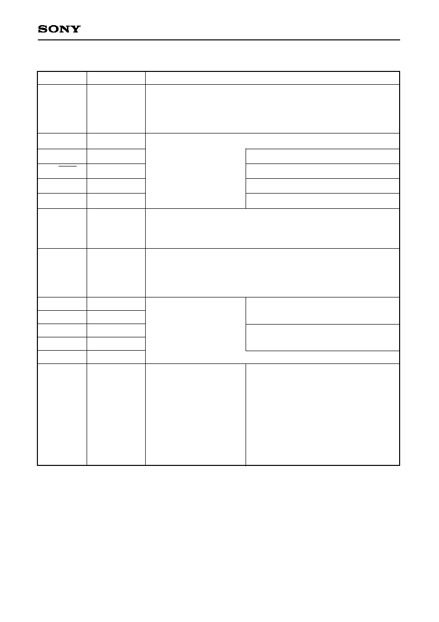
(Port A)
8-bit I/O port. I/O can be set in a unit of single bits.
Incorporation of pull-up resistor can be set through the program in a unit of
single bits.
(8 pins)
(Port C)
8-bit I/O port. I/O can be set in a unit of single bits. Incorporation of pull-up
resistor can be set through the program in a unit of single bits.
(8 pins)
(Port D)
8-bit I/O port. I/O can be set in a unit of single bits. Can drive 12mA sink
current. Incorporation of pull-up resistor can be set through the program in a
unit of single bits.
(8 pins)
(Port E)
8-bit port. Lower 2 bits are
for input; upper 6 bits are for
output.
(8 pins)
(Port F)
8-bit I/O port. PF4 to PF7
can be set in a unit of single
bits as standby release
inputs. I/O can be set in a
unit of single bits.
Incorporation of pull-up
resistor can be set through
the program in a unit of
single bits.
(8 pins)
Analog inputs to A/D converter.
(8 pins)
Pin Description
Symbol
PA0 to PA7
PC0 to PC7
PD0 to PD7
PE0/INT0
PE1/INT1
PE2/PWM0
PE3/PWM1
PE4 to PE7
PF0/AN4
to
PF7/AN11
I/O
I/O
I/O
Input/Input
Input/Input
Output/Output
Output/Output
Output
I/O
I/O
Description
(Port B)
8-bit I/O port. I/O can be set
in a unit of single bits.
Incorporation of pull-up
resistor can be set through
the program in a unit of
single bits.
(8 pins)
External interrupt inputs.
(2 pins)
12-bit PWM outputs.
(2 pins)
16-bit timer/counter rectangular wave output.
Serial clock I/O (CH2).
Serial data output (CH2).
Serial data input (CH2).
I/O
I/O/Output
I/O/I/O
I/O/Output
I/O/Input
PB0 to PB3
PB4/TO2
PB5/SCK2
PB6/SO2
PB7/SI2