CMOS 8-bit Single Chip Microcomputer
Description
The CXP7400P10 is a CMOS 8-bit microcomputer
integrating on a single chip an A/D converter, serial
interface, timer/counter, time-base timer, capture
timer/counter, remote control receive circuit, PWM
output, and the like besides the basic configurations
of 8-bit CPU, ROM, RAM, and I/O port.
The CXP7400P10 also provides the sleep/stop
functions that enable lower power consumption.
The CXP7400P10 is the PROM-incorporated
version of the CXP740056/740096/740010 with built-
in mask ROM. This provides the additional feature of
being able to write directly into the program. Thus, it
is most suitable for evaluation use during system
development and for small-quantity production.
Features
∑ A wide instruction set (211 instructions) which covers various types of data.
-- 16-bit arithmetic/multiplication and division/Boolean bit operation instructions
∑ Minimum instruction cycle
167ns at 24MHz operation (4.5 to 5.5V)
333ns at 12MHz operation (2.7 to 5.5V)
122µs at 32kHz operation (2.7 to 5.5V)
∑ Incorporated PROM capacity
120K bytes
∑ Incorporated RAM capacity
4096 bytes
∑ Peripheral functions
-- A/D converter
8 bits, 8 channels, successive approximation method
(Conversion time 10.3µs at 24MHz)
-- Serial interface
Srart-stop synchronization (UART), 1 channel
Incorporated buffer RAM (Auto transfer for 1 to 32 bytes), 2 channels
8-bit clock syncronization (MSB/LSB first selectable), 1 channel
-- Timer
8-bit timer 2 channels, 8-bit timer/counter 2 channels,
19-bit time-base timer, 16-bit capture timer/counter
32kHz timer/counter
-- Remote control receive circuit
Noise elimination circuit
8-bit pulse measuring counter, 6-stage FIFO
-- PWM output
12 bits, 2 channels
∑ Interruption
22 factors, 15 vectors, multi-interruption possible
∑ Standby mode
Sleep/stop
∑ Package
100-pin plastic QFP/LQFP
≠ 1 ≠
E98518-PS
Sony reserves the right to change products and specifications without prior notice. This information does not convey any license by
any implication or otherwise under any patents or other right. Application circuits shown, if any, are typical examples illustrating the
operation of the devices. Sony cannot assume responsibility for any problems arising out of the use of these circuits.
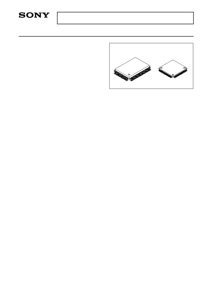
CXP7400P10
100 pin QFP (Plastic)
100 pin LQFP (Plastic)
Structure
Silicon gate CMOS IC
≠ 2 ≠
CXP7400P10
P
F
0
t
o
P
F
7
8
R
A
M
4
0
9
6
B
Y
T
E
S
IN
TE
RR
UP
T C
ON
TR
OL
LE
R
A
/
D
C
O
N
V
E
R
T
E
R
IN
T3
IN
T1
IN
T0
IN
T2
A
N
0
t
o
A
N
1
1
1
2
RS
T
V
DD
V
SS
EX
TA
L
XT
AL
AV
RE
F
AV
SS
R
x
D
T
x
D
P
R
O
M
1
2
0
K
B
Y
T
E
S
2
C
L
O
C
K
G
E
N
E
R
A
T
O
R
/
S
Y
S
T
E
M
C
O
N
T
R
O
L
PO
RT
A
2
6
P
A
0
t
o
P
A
7
P
B
0
t
o
P
B
7
P
C
0
t
o
P
C
7
P
D
0
t
o
P
D
7
P
E
0
t
o
P
E
1
P
E
2
t
o
P
E
7
P
G
0
t
o
P
G
7
P
I
1
t
o
P
I
7
PO
RT
B
PO
RT
C
PO
RT
D
PO
RT
E
PO
RT
F
PO
RT
G
PO
RT
I
P
H
0
t
o
P
H
7
PO
RT
H
U
A
R
T
R
E
C
E
I
V
E
R
U
A
R
T
T
R
A
N
S
M
I
T
T
E
R
U
A
R
T
B
A
U
D
R
A
T
E
G
E
N
E
R
A
T
O
R
8
8
8
8
8
7
IN
T4
NM
I
2
P
W
M
0
1
2
-
B
I
T
P
W
M
G
E
N
E
R
A
T
O
R
0
1
2
-
B
I
T
P
W
M
G
E
N
E
R
A
T
O
R
1
P
W
M
1
R
E
M
O
C
O
N
I
N
B
U
F
F
E
R
R
A
M
C
S
0
S
I
0
S
O
0
S
C
K
0
S
E
R
I
A
L
I
N
T
E
R
F
A
C
E
U
N
I
T
(
C
H
1
)
1
6
-
B
I
T
C
A
P
T
U
R
E
T
I
M
E
R
/
C
O
U
N
T
E
R
4
T
O
2
8
-
B
I
T
T
I
M
E
R
/
C
O
U
N
T
E
R
0
8
-
B
I
T
T
I
M
E
R
1
E
C
0
C
I
N
T
E
C
2
S
E
R
I
A
L
I
N
T
E
R
F
A
C
E
U
N
I
T
(
C
H
2
)
S
I
2
S
O
2
S
C
K
2
P
J
0
t
o
P
J
7
PO
RT
J
8
AV
DD
R
M
C
C
S
1
S
I
1
S
O
1
S
C
K
1
P
R
E
S
C
A
L
E
R
/
T
I
M
E
-
B
A
S
E
T
I
M
E
R
B
U
F
F
E
R
R
A
M
TX
TE
X
3
2
k
H
z
T
I
M
E
R
/
C
O
U
N
T
E
R
2
5
P
O
R
T
K
PK
3 t
o P
K7
PK
1 t
o P
K2
F
I
F
O
S
E
R
I
A
L
I
N
T
E
R
F
A
C
E
U
N
I
T
(
C
H
0
)
T
O
0
8
-
B
I
T
T
I
M
E
R
/
C
O
U
N
T
E
R
2
8
-
B
I
T
T
I
M
E
R
3
E
C
1
T
O
1
2
A
D
J
Vp
p
S
P
C
7
0
0
I
I
C
P
U
C
O
R
E
8
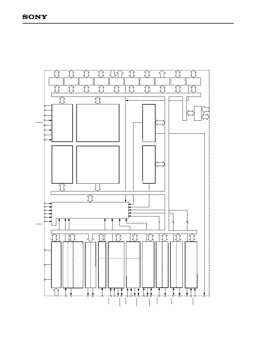
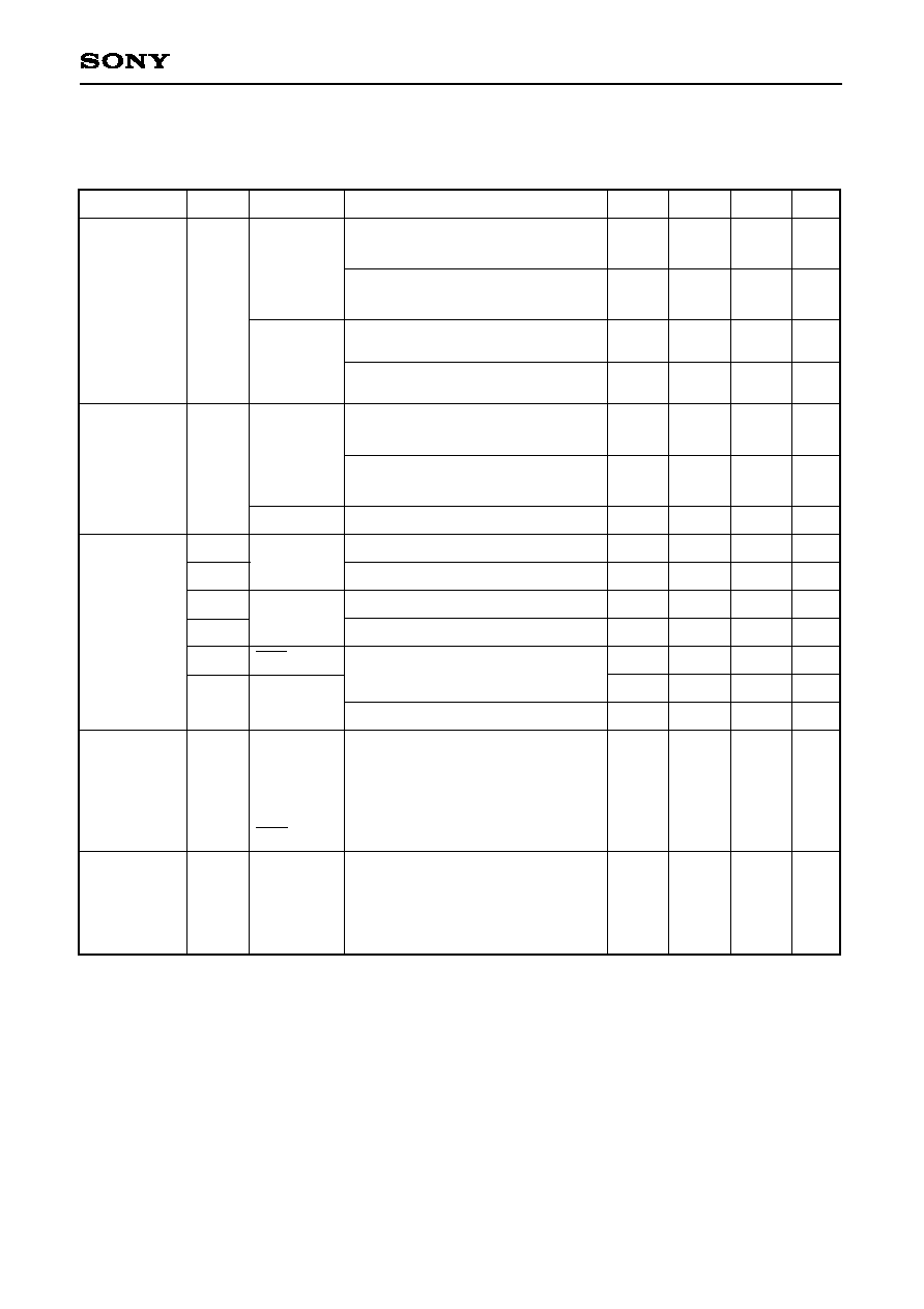
Block Diagram
≠ 3 ≠
CXP7400P10
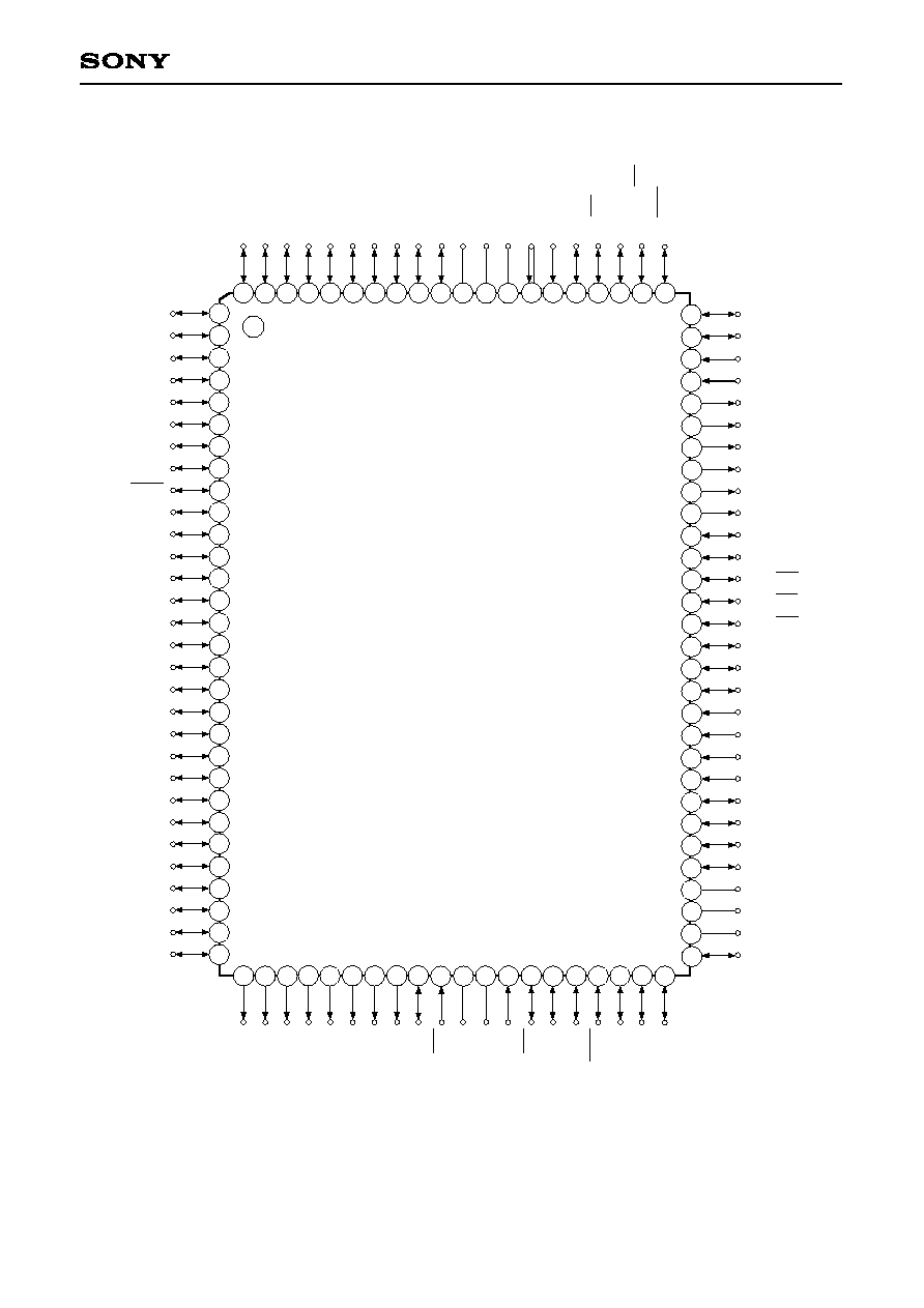
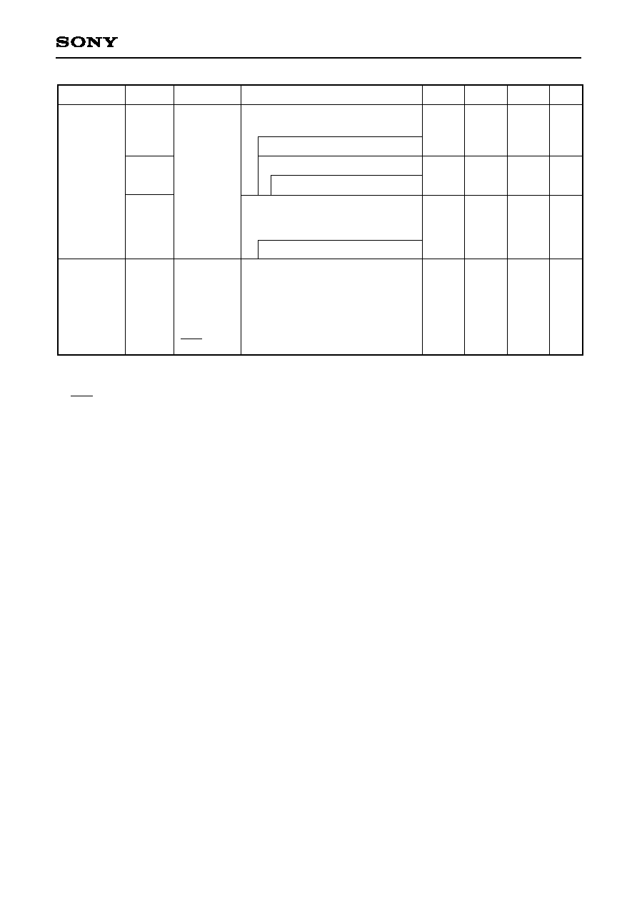
Pin Assignment (Top View) 100-pin QFP package
2
3
4
5
6
7
8
9
10
11
12
13
14
15
16
17
18
19
20
21
22
23
24
25
26
27
28
29
30
40
39
38
37
36
35
34
31 32 33
41 42 43 44 45 46 47 48 49 50
51
52
53
54
55
56
57
58
59
60
70
69
68
67
63
64
65
66
61
62
71
72
73
74
81
82
83
84
75
76
77
78
88 87 86 85
79
89
90
100 99 98 97 96 95 94
91
92
93
1
80
PI6/SO1
PI7/SI1
PE0/INT0
PE1/INT2
PE2/PWM0
PE3/PWM1
PE4
PE5
PE6
PE7
PG0/TxD
PG1/RxD
PG2/EC0
PG3/EC1
PG4/EC2
PG5/INT3
PG6/INT4
PG7/CINT
AN0
AN1
AN2
AN3
PF0/AN4
PF1/AN5
PF2/AN6
PF3/AN7
AV
DD
AV
REF
AV
SS
PF4/AN8
PC5
PC4
PC3
PC2
PC1
PC0
PB7/SI2
PB6/SO2
PB5/SCK2
PB4/TO2
PB3
PB2
PB1
PB0
PJ7
PJ6
PJ5
PJ4
PJ3
PJ2
PJ1
PJ0
PD7
PD6
PD5
PD4
PD3
PD2
PD1
PD0
P
C
6
P
C
7
P
A
0
P
A
1
P
A
2
P
A
3
P
A
4
P
A
5
P
A
6
P
A
7
V
p
p
V
D
D
V
S
S
P
K
1
/
T
X
P
K
2
/
T
E
X
P
I
1
/
R
M
C
P
I
2
/
N
M
I
P
I
3
/
T
O
0
/
A
D
J
P
I
4
/
I
N
T
1
/
C
S
1
P
I
5
/
S
C
K
1
P
H
7
P
H
6
P
H
5
P
H
4
P
H
3
P
H
2
P
H
1
P
H
0
P
K
7
/
T
O
1
R
S
T
V
S
S
X
T
A
L
E
X
T
A
L
P
K
6
/
C
S
0
P
K
5
/
S
I
0
P
K
4
/
S
O
0
P
K
3
/
S
C
K
0
P
F
7
/
A
N
1
1
P
F
6
/
A
N
1
0
P
F
5
/
A
N
9
Note) 1. Vpp (Pin 90) is left open.
2. V
SS
(Pins 41 and 88) are both connected to GND.
≠ 4 ≠
CXP7400P10
2
3
4
5
6
7
8
9
10
11
12
13
14
15
16
17
18
19
20
21
22
23
24
25
40
39
38
37
36
35
34
31 32 33
41 42 43 44 45 46 47 48 49 50
51
52
53
54
55
56
57
58
59
60
70
69
68
67
63
64
65
66
61
62
71
72
73
74
81
82
83
84
75
76
77
78
88 87 86 85
79
89
90
100 99 98 97 96 95 94
91
92
93
1
80
P
I
6
/
S
O
1
P
I
7
/
S
I
1
P
E
0
/
I
N
T
0
PE1/INT2
PE2/PWM0
PE3/PWM1
PE4
PE5
PE6
PE7
PG0/TxD
PG1/RxD
PG2/EC0
PG3/EC1
PG4/EC2
PG5/INT3
PG6/INT4
PG7/CINT
AN0
AN1
AN2
AN3
PF0/AN4
PF1/AN5
PF2/AN6
PC3
PC2
PC1
PC0
PB7/SI2
PB6/SO2
PB5/SCK2
PB4/TO2
PB3
PB2
PB1
PB0
PJ7
PJ6
PJ5
PJ4
PJ3
PJ2
PJ1
PJ0
PD7
PD6
PD5
P
C
6
P
C
7
P
A
0
P
A
1
P
A
2
P
A
3
P
A
4
P
A
5
P
A
6
P
A
7
V
p
p
V
D
D
V
S
S
P
K
1
/
T
X
P
K
2
/
T
E
X
P
I
1
/
R
M
C
P
I
2
/
N
M
I
P
I
3
/
T
O
0
/
A
D
J
P
I
4
/
I
N
T
1
/
C
S
1
P
I
5
/
S
C
K
1
P
H
2
P
H
1
P
H
0
P
K
7
/
T
O
1
R
S
T
V
S
S
X
T
A
L
E
X
T
A
L
P
K
6
/
C
S
0
P
K
5
/
S
I
0
P
K
4
/
S
O
0
P
K
3
/
S
C
K
0
P
F
7
/
A
N
1
1
P
F
6
/
A
N
1
0
P
F
5
/
A
N
9
P
H
7
P
H
6
P
H
5
P
H
4
P
H
3
26 27 28 29 30
PD4
PD3
P
D
2
P
D
1
P
D
0
P
F
4
/
A
N
8
A
V
S
S
PF3/AN7
AV
DD
AV
REF
P
C
4
P
C
5
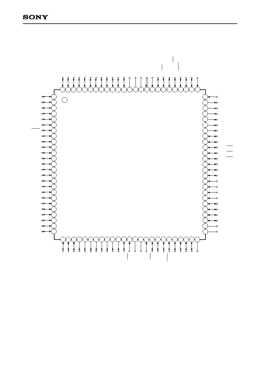
Pin Assignment (Top View) 100-pin LQFP package
Note) 1. Vpp (Pin 88) is left open.
2. V
SS
(Pins 39 and 86) are both connected to GND.
≠ 5 ≠
CXP7400P10
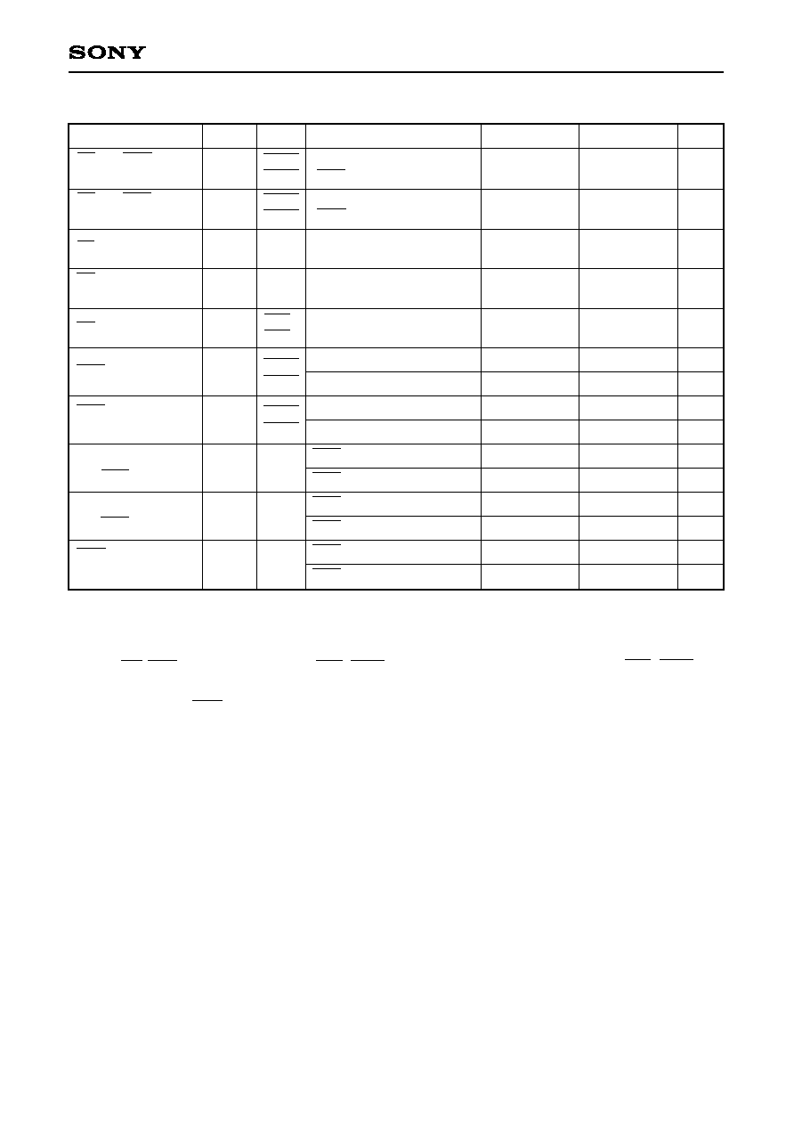
(Port A)
8-bit I/O port. I/O can be set in a unit of single bits.
Incorporation of pull-up resistor can be set through the program in a unit of
single bits.
(8 pins)
(Port C)
8-bit I/O port. I/O can be set in a unit of single bits. Incorporation of pull-up
resistor can be set through the program in a unit of single bits.
(8 pins)
(Port D)
8-bit I/O port. I/O can be set in a unit of single bits. Can drive 12mA sink
current. Incorporation of pull-up resistor can be set through the program in a
unit of single bits.
(8 pins)
(Port E)
8-bit port. Lower 2 bits are
for input; upper 6 bits are for
output.
(8 pins)
(Port F)
8-bit I/O port. I/O can be set
in a unit of single bits.
PF4 to PF7 can be set in a
unit of single bits as standby
release inputs.
Incorporation of pull-up
resistor can be set through
the program in a unit of
single bits.
(8 pins)
Analog inputs to A/D converter.
(8 pins)
Pin Description
Symbol
PA0 to PA7
PC0 to PC7
PD0 to PD7
PE0/INT0
PE1/INT2
PE2/PWM0
PE3/PWM1
PE4 to PE7
PF0/AN4
to
PF7/AN11
I/O
I/O
I/O
Input/Input
Input/Input
Output/Output
Output/Output
Output
I/O/Input
I/O
Description
(Port B)
8-bit I/O port. I/O can be set
in a unit of single bits.
Incorporation of pull-up
resistor can be set through
the program in a unit of
single bits.
(8 pins)
External interrupt inputs.
(2 pins)
12-bit PWM outputs.
(2 pins)
16-bit timer/counter rectangular wave output.
Serial clock I/O (CH2).
Serial data output (CH2).
Serial data input (CH2).
I/O
I/O/Output
I/O/I/O
I/O/Output
I/O/Input
PB0 to PB3
PB4/TO2
PB5/SCK2
PB6/SO2
PB7/SI2
≠ 6 ≠
CXP7400P10
(Port H)
8-bit output port. Operated as N-ch open drain output for medium voltage
drive (12V) and large current (12mA).
(8 pins)
(Port I)
7-bit I/O port. I/O can be set
in a unit of single bits.
Incorporation of pull-up
resistor can be set through
the program in a unit of
single bits.
(7 pins)
(Port J)
8-bit I/O port. I/O can be set in a unit of single bits.
Standby release input can be set in a unit of single bits.
Incorporation of pull-up resistor can be set through the program in a unit of
single bits.
(8 pins)
(Port K)
7-bit port. Lower 2 bits are for
input; upper 5 bits are for I/O.
I/O can be set in a unit of
single bits.
For PK3 to PK7, incorporation
of pull-up resistor can be set
through the program in a unit
of single bits.
(7 pins)
UART transmission data output.
UART reception data input.
External event input for 8-bit timer/counter 0.
External event input for 8-bit timer/counter 2.
External event input for 16-bit timer/counter.
External capture input to 16-bit timer/counter.
Remote control receiver circuit input.
Non-maskable interrupt input.
Output for the 8-bit timer/counter 1
rectanguler waves and TEX oscillation
frequency demultiplication.
Serial clock I/O (CH1).
Serial data output (CH1).
Serial data input (CH1).
Crystal connectors for 32-kHz timer/counter
clock oscillation circuit.
For usage as event counter, connect clock
oscillation source to TEX, and leave TX
open.
Serial clock I/O (CH0).
Serial data output (CH0).
Serial data input (CH0).
Chip select input for serial inteface (CH0).
8-bit timer/counter 3 rectangular wave output.
Symbol
PG0/TxD
PG1/RxD
PG2/EC0
PG3/EC1
PG4/EC2
PG5/INT3
PG6/INT4
PG7/CINT
PH0 to PH7
PI1/RMC
PI2/NMI
PI3/TO0/
ADJ
PI4/INT1/
CS1
PI5/SCK1
PI6/SO1
PI7/SI1
PJ0 to PJ7
PK3/SCK0
PK4/SO0
PK5/SI0
PK6/CS0
PK7/TO1
I/O/Output
I/O/Input
I/O/Input
I/O/Input
I/O/Input
I/O/Input
I/O/Input
I/O/Input
Output
I/O/Input
I/O/Input
I/O/Output/
Output
I/O/Input/
Input
I/O/I/O
I/O/Output
I/O/Input
I/O
I/O/I/O
I/O/Output
I/O/Input
I/O/Input
I/O/Output
I/O
Description
Chip select input for serial
interface (CH1).
External
interrupt input.
(Port G)
8-bit I/O port. I/O can be set
in a unit of single bits.
Incorporation of pull-up
resistor can be set through
the program in a unit of
single bits.
(8 pins)
PK1/TX
PK2/TEX
Input
Input/Input
External interrupt inputs.
(2 pins)
≠ 7 ≠
CXP7400P10
Analog inputs to A/D converter.
(4 pins)
Connects a crystal for system clock oscillation. When a clock is supplied
externally, input it to EXTAL pin and input a reversed phase clock to XTAL
pin.
System reset; active at Low level.
Positive power supply pin for incorporated PROM writing.
Leave this pin open for normal operation.
(Connected to V
DD
internally.)
Positive power supply of A/D converter.
Reference voltage input of A/D converter.
GND of A/D converter.
Positive power supply.
GND. Connect both V
SS
pins to GND.
Symbol
I/O
Description
EXTAL
XTAL
Input
AN0 to AN3
RST
Vpp
AV
DD
AV
REF
AV
SS
V
DD
V
SS
Input
Input
Input
≠ 8 ≠
CXP7400P10
18 pins
Hi-Z
Hi-Z
After a reset
PA0 to PA7
PB0
PB2
PC0 to PC7
PB4/TO2
PI3/TO0/ADJ
PK7/TO1
3 pins
Internal data bus
RD (Ports A, B, C)
IP
Ports A, B, C data
"0" after a reset
Ports A, B, C direction
Pull-up resistor
"0" after a reset
Pull-up transistors
approx. 100k
(V
DD
= 4.5 to 5.5V)
approx. 150k
(V
DD
= 2.7 to 3.3V)
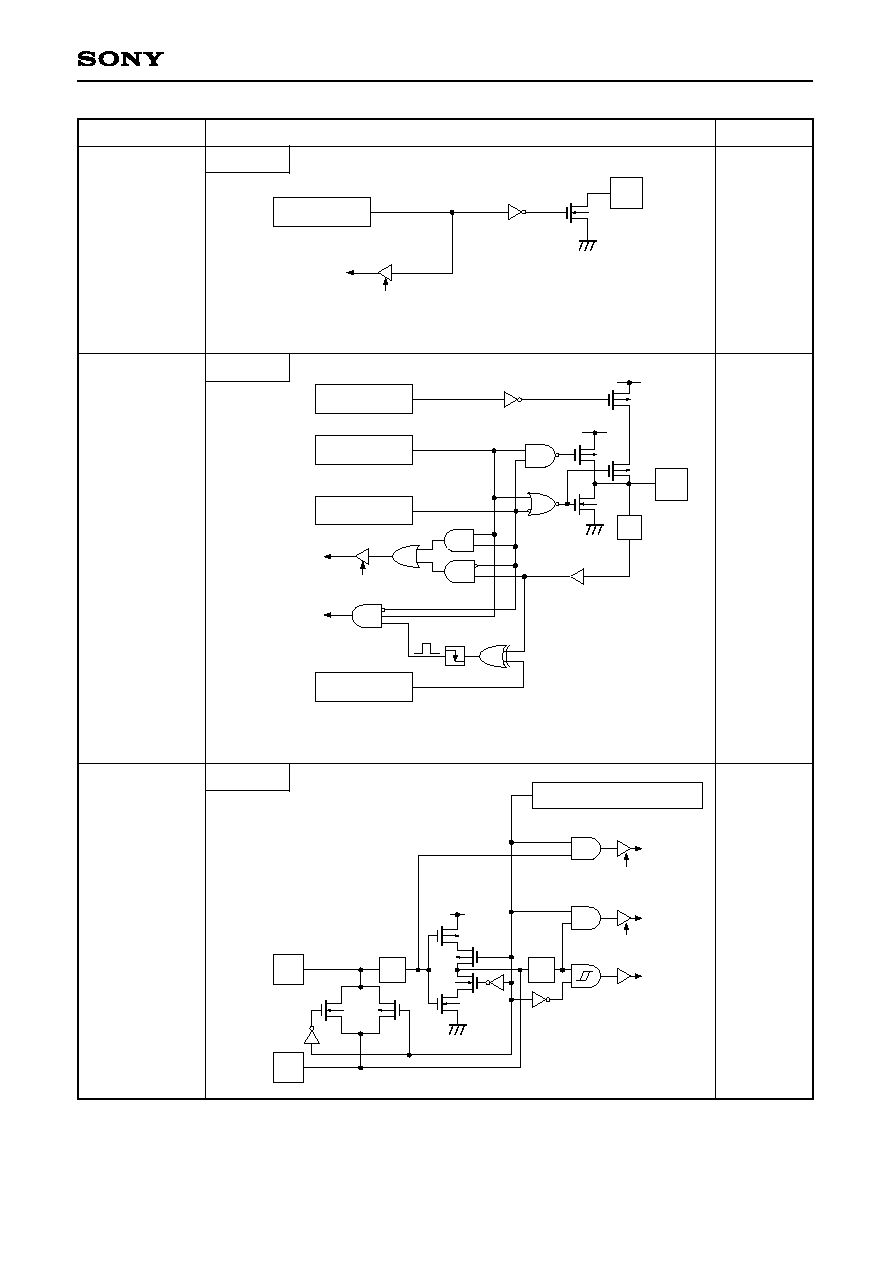
I/O Circuit Format for Pins
Pin
Circuit format
2 pins
Hi-Z
PB1
PB3
Internal data bus
RD (Port B)
IP
Port B data
"0" after a reset
Port B direction
Pull-up resistor
"0" after a reset
Pull-up transistors
approx. 100k
(V
DD
= 4.5 to 5.5V)
approx. 150k
(V
DD
= 2.7 to 3.3V)
Schmitt input
Internal
data bus
RD (Ports B, I, K)
IP
Ports B, I, K function
select
"0" after a reset
"0" after a reset
Pull-up resistor
TO2, TO0/ADJ, TO1
"0" after a reset
Pull-up transistors
approx. 100k
(V
DD
= 4.5 to 5.5V)
approx. 150k
(V
DD
= 2.7 to 3.3V)
Ports B, I, K data
Ports B, I, K direction
Port A
Port B
Port C
Port B
PortB
Port K
Port I
≠ 9 ≠
CXP7400P10
3 pins
Hi-Z
Hi-Z
After a reset
PB5/SCK2
PI5/SCK1
PK3/SCK0
PB6/SO2
PG0/TxD
PI6/SO1
PK4/SO0
4 pins
Internal
data bus
RD (Ports B, I, K)
IP
Ports B, I, K direction
"0" after a reset
Pull-up transistors
approx. 100k
(V
DD
= 4.5 to 5.5V)
approx. 150k
(V
DD
= 2.7 to 3.3V)
Ports B, I, K data
"0" after a reset
Ports B, I, K function
select
SCK2, SCK1, SCK0
Output enable
Output buffer
capability
"0" after a reset
Pull-up resistor
"0" after a reset
Schmitt input
SCK2, SCK1, SCK0
Pin
Circuit format
Internal
data bus
RD (Ports B, G, I, K)
IP
Ports B, G, I, K
direction
"0" after a reset
Pull-up transistors
approx. 100k
(V
DD
= 4.5 to 5.5V)
approx. 150k
(V
DD
= 2.7 to 3.3V)
Ports B, G, I, K data
"0" after a reset
Ports B, G, I, K
function select
SO2, TxD, SO1, SO0
Output enable
Output buffer
capability
"0" after a reset
Pull-up resistor
"0" after a reset
Port B
Port I
Port K
Port B
Port G
Port I
Port K
≠ 10 ≠
CXP7400P10
14 pins
Hi-Z
Hi-Z
After a reset
PB7/SI2
PG1/RxD
PG2/EC0
PG3/EC1
PG4/EC2
PG5/INT3
PG6/INT4
PG7/CINT
PI1/RMC
PI2/NMI
PI4/INT1/CS1
PI7/SI1
PK5/SI0
PK6/CS0
PE0/INT0
PE1/INT2
2 pins
Internal data bus
RD (Ports B, G, I, K)
Ports B, G, I, K direction
IP
Ports B, G, I, K data
Pull-up resistor
"0" after a reset
"0" after a reset
Schmitt input
SI2, RxD, EC0, EC1, EC2, INT3, INT4, CINT,
RMC, NMI, INT1/CS1, SI1, SI0, CS0
Pull-up transistors
approx. 100k
(V
DD
= 4.5 to 5.5V)
approx. 150k
(V
DD
= 2.7 to 3.3V)
Pin
Circuit format
8 pins
Hi-Z
PD0 to PD7
Internal data bus
RD (Port D)
Port D direction
Port D data
Pull-up resistor
"0" after a reset
2
1
1
Large current
12mA (V
DD
= 4.5 to 5.5V)
4.5mA (V
DD
= 2.7 to 3.3V)
2
Pull-up transistors
approx. 100k
(V
DD
= 4.5 to 5.5V)
approx. 150k
(V
DD
= 2.7 to 3.3V)
IP
IP
Schmitt input
RD (Port E)
Internal data bus
INT0, INT2
Port B
Port G
Port I
Port K
Port D
Port E
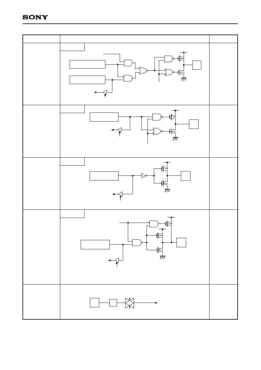
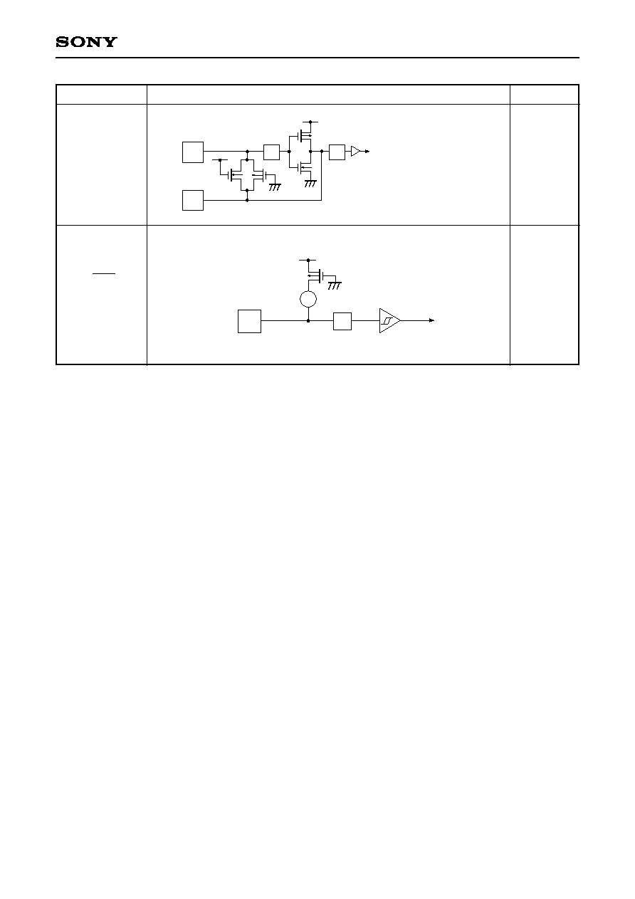
≠ 11 ≠
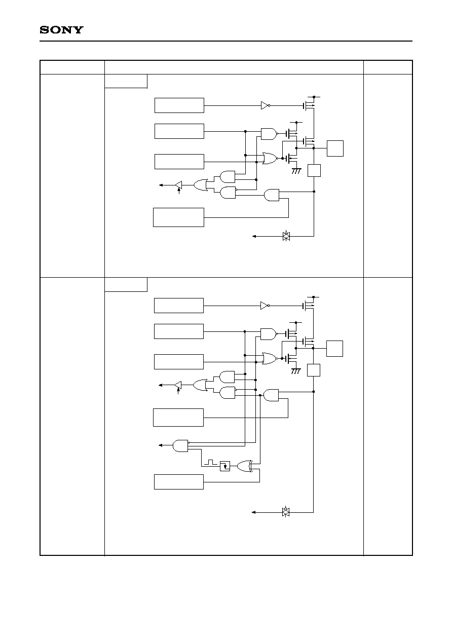
CXP7400P10
2 pins
Hi-Z
After a reset
PE2/PWM0
PE3/PWM1
Port E function select
"0" after a reset
PWM0, PWM1
Port E data
Internal data bus
RD (Port E)
Hi-Z by writing to Port E data register or Port E
function select register
Output active
2 pins
Hi-Z
PE4
PE5
Hi-Z by writing to Port E data
register
Output active
Internal data bus
RD (Port E)
Port E data
1 pin
"H" level
PE6
Internal data bus
RD (Port E)
Port E data
"1" after a reset
1 pin
PE7
Internal data bus
RD (Port E)
Pull-up transistors
approx. 150k
(V
DD
= 4.5 to 5.5V)
approx. 200k
(V
DD
= 2.7 to 3.3V)
Internal reset signal
Port E data
"1" after a reset
4 pins
Hi-Z
AN0 to AN3
IP
A/D converter
Input multiplexer
Pin
Circuit format
"H" level
"H" level
at ON
resistance
of pull-up
transistor
during a
reset.
)
Port E
Port E
Port E
Port E
)
≠ 12 ≠
CXP7400P10
4 pins
Hi-Z
Hi-Z
After a reset
PF0/AN4
to
PF3/AN7
PF4/AN8
to
PF7/AN11
4 pins
Internal data bus
RD (Port F)
Port F direction
IP
Port F data
Pull-up resistor
Port F
function select
"0" after a reset
"0" after a reset
"0" after a reset
Input multiplexer
A/D converter
Pull-up transistors
approx. 100k
(V
DD
= 4.5 to 5.5V)
approx. 150k
(V
DD
= 2.7 to 3.3V)
Pin
Circuit format
Internal data bus
RD (Port F)
Port F direction
IP
Port F data
Pull-up resistor
Port F
function select
"0" after a reset
"0" after a reset
"0" after a reset
Input multiplexer
A/D converter
Pull-up transistors
approx. 100k
(V
DD
= 4.5 to 5.5V)
approx. 150k
(V
DD
= 2.7 to 3.3V)
Polarity select
"0" after a reset
Edge detection
Standby release
Port F
Port F
≠ 13 ≠
CXP7400P10
8 pins
Hi-Z
Hi-Z
After a reset
PH0 to PH7
PJ0 to PJ7
8 pins
Internal data bus
RD (Port H)
Port H data
"1" after a reset
High tension proof 12V
Large current
12mA (V
DD
= 4.5 to 5.5V)
4.5mA (V
DD
= 2.7 to 3.3V)
Pin
Circuit format
Internal data bus
RD (Port J)
Port J direction
IP
Port J data
Pull-up resistor
"0" after a reset
"0" after a reset
Pull-up transistors
approx. 100k
(V
DD
= 4.5 to 5.5V)
approx. 150k
(V
DD
= 2.7 to 3.3V)
Polarity select
"0" after a reset
Edge detection
Standby release
Oscillation
stop port
input
PK1/TX
PK2/TEX
2 pins
IP
IP
TEX oscillation circuit control
RD (Port K)
Schmitt input
Clock input
Internal
data bus
Internal
data bus
"1" after a reset
PK2/TEX
PK1/TX
RD (Port K)
Port H
Port J
Port K
≠ 14 ≠
CXP7400P10
2 pins
Oscillation
After a reset
EXTAL
XTAL
IP
EXTAL
XTAL
∑ Diagram shows circuit configuration
during oscillation.
∑ When program stops the oscillation,
the feedback registor disconnects,
and XTAL is driven at "H" level.
IP
1 pin
"L" level
(during a
reset)
RST
Schmitt input
Pull-up resistor
Mask option OP
IP
Pin
Circuit format

≠ 15 ≠
CXP7400P10
Supply voltage
Input voltagte
Output voltage
High level output current
High level total output current
Low level output current
Low level total output current
Operating temperature
Storage temperature
Allowable power dissipation
1
AV
DD
and V
DD
must be set to the same voltage.
2
V
IN
and V
OUT
must not exceed V
DD
+ 0.3V.
3
The large current output pins are Port D and H (PD, PH).
Note) Usage exceeding absolute maximum ratings may permanently impair the LSI. Normal operation should
be conducted under the recommended operating conditions. Exceeding these conditions may adversely
affect the reliability of the LSI.
V
DD
Vpp
AV
DD
AV
SS
AV
REF
V
IN
V
OUT
I
OH
I
OH
I
OL
I
OLC
I
OL
Topr
Tstg
P
D
≠0.3 to +7.0
≠0.3 to +13.0
AV
SS
to +7.0
1
≠0.3 to +0.3
AV
SS
to +7.0
≠0.3 to +7.0
2
≠0.3 to +7.0
2
≠5
≠50
15
20
100
≠20 to +75
≠55 to +150
600
380
V
V
V
V
V
V
V
mA
mA
mA
mA
mA
∞C
∞C
mW
Incorporated PROM
Output (value per pin)
Total for all output pins
All pins excluding large current
outputs (value per pin)
Large current outputs (value per pin)
3
Total for all output pins
QFP package
LQFP package
Item
Symbol
Rating
Unit
Remarks
Absolute Maximum Ratings
(Vss = 0V reference)
≠ 16 ≠
CXP7400P10
High level input
voltage
Low level input
voltage
Operating temperature
Supply voltage
Analog voltage
5.5
5.5
V
DD
V
DD
V
DD
V
DD
+ 0.3
V
DD
+ 0.2
0.3V
DD
0.2V
DD
0.2V
DD
0.4
0.2
+75
V
V
V
V
V
V
V
V
V
V
∞C
V
V
V
V
Item
Symbol
Min.
4.5
2.7
5.5
5.5
Max.
Unit
Remarks
fc = 24MHz or less Guaranteed operation
range for 1/2 and 1/4
frequency dividing clock
fc = 12MHz or less
V
2.7
5.5
2.5
2.7
0.7V
DD
0.8V
DD
0.8V
DD
V
DD
≠ 0.4
V
DD
≠ 0.2
0
0
0
≠0.3
≠0.3
≠20
V
IH
V
IHS
V
IHEX
V
IL
V
ILS
V
ILEX
Topr
Guaranteed operation range for 1/16
frequency dividing clock or sleep mode
Guarantteed operaion range for TEX
Guaranteed data hold operation range
during stop mode
1
2
,
6
2
,
7
Hysteresis input
3
EXTAL pin
4,
6
, TEX pin
5,
6
EXTAL pin
4,
7
, TEX pin
5,
7
2,
6
2,
7
Hysteresis input
3
EXTAL pin
4,
6
, TEX pin
5,
6
EXTAL pin
4,
7
, TEX pin
5,
7
V
DD
AV
DD
1
AV
DD
and V
DD
must be set to the same voltage.
2
Normal input port (PA, PB0, PB2, PB4, PB6, PC, PD, PF, PG0, PI3, PI6, PJ, PK1, PK2, PK4, PK7)
3
RST, PB1, PB3, PB5/SCK2, PB7/SI2, PE0/INT0, PE1/INT2, PG1/RxD, PG2/EC0, PG3/EC1, PG4/EC2,
PG5/INT3, PG6/INT4, PG7/CINT, PI1/RMC, PI2/NMI, PI4/INT1/CS1, PI5/SCK1, PI7/SI1, PK3/SCK0,
PK5/SI0, PK6/CS0
4
Specifies only when the external clock is input.
5
Specifies only when the external event count is input.
6
This case applies to the range of 4.5 to 5.5V supply voltage (V
DD
).
7
This case applies to the range of 2.7 to 5.5V supply voltage (V
DD
).
Recommended Operating Conditions
(Vss = 0V reference)
2.7
5.5
V

≠ 17 ≠
CXP7400P10
V
DD
= 4.5V, I
OL
= 12.0mA
V
DD
= 5.5V, V
IH
= 5.5V
V
DD
= 5.5V, V
IL
= 0.4V
V
DD
= 5.5V, V
IL
= 5.5V
V
DD
= 5.5V, V
IL
= 0.4V
V
DD
= 5.5V, V
IL
= 0.4V
V
DD
= 4.5V, V
IL
= 4.0V
V
DD
= 5.5V
V
I
= 0, 5.5V
V
DD
= 5.5V
V
OH
= 12V
High level
output voltage
Low level
output voltage
Input current
I/O leakage
current
0.5
≠0.5
0.1
≠0.1
≠1.5
≠2.78
V
V
V
V
V
µA
µA
µA
µA
µA
µA
µA
µA
µA
PD, PH
PA to PD,
PE2 to PE7,
PF to PG,
PI to PJ,
PK3 to PK7
PB5, PB6
1
,
PG0
1
,
PI5, PI6
1
,
PK3, PK4
1
PA to PD,
PE2 to PE7,
PF to PG,
PI to PJ,
PK3 to PK7
EXTAL
TEX
RST
2
PA to PD
3
,
PF to PG
3
,
PI to PK
3
Item
Symbol
Pins
Conditions
Min.
PA to PD
3
,
PF to PG
3
,
PI to PK
3
,
PE,
AN0 to AN3
RST
2
PH
Typ.
1.5
40
≠40
10
≠10
≠400
≠45
±10
50
Max.
Unit
DC Characteristics (V
DD
= 4.5 to 5.5V)
Electrical Characteristics
(Ta = ≠20 to +75∞C, V
SS
= 0V reference)
V
OH
V
OL
I
IHE
I
ILE
I
IHT
I
ILT
I
ILR
I
IL
I
IZ
Open drain
output leakage
current
(N-ch Tr off
state)
L
LOH
V
DD
= 4.5V, I
OH
= ≠1.0mA
V
DD
= 4.5V, I
OH
= ≠1.2mA
V
DD
= 4.5V, I
OH
= ≠0.5mA
4.0
3.5
4.0
3.5
0.4
0.6
V
V
V
DD
= 4.5V, I
OH
= ≠2.4mA
V
DD
= 4.5V, I
OL
= 1.8mA
V
DD
= 4.5V, I
OL
= 3.6mA
≠ 18 ≠
CXP7400P10
Supply
current
4
Item
Symbol
Pins
Conditions
Min.
50
62
mA
mA
µA
µA
43
1.8
9.0
80
µA
13
40
10
PA to PD,
PE0 to PE1,
PF to PG,
PI to PK,
AN0 to AN3,
EXTAL,
RST
Clock 1MHz
0V for all pins excluding measured
pins
V
DD
= 5V ± 0.5V
Sleep mode
V
DD
= 5V ± 0.5V
24MHz crystal oscillation
(C
1
= C
2
= 15pF)
V
DD
I
DD1
I
DDS1
I
DD2
I
DDS2
I
DDS3
C
IN
Typ.
Max.
Unit
1
This case applies that Port B buffer capability switching register (BUFB: 010F4h, bits 6 and 5 = "1, 1") and
Ports G/I/K buffer capability switching register (BUFG: 010F5h, bits 0, 3, 4, 5 and 6 = "1, 1, 1, 1, 1") are ON.
2
RST pin specifies the input current when the pull-up resistor is selected, and specifies the leakage current
when no resistor is selected.
3
PA to PD, PF to PG and PI to PK pins specify the input current when the pull-up resistor is selected, and
specify the leakage current when no resistor is selected.
4
When all output pins are open.
V
DD
= 3V ± 0.3V
Sleep mode
V
DD
= 3V ± 0.3V
32kHz crystal oscillation
(C
1
= C
2
= 47pF)
Stop mode
(Termination of EXTAL and TEX pins
crystal oscillation)
V
DD
= 5V ± 0.5V
Input
capacity
pF
20
10
≠ 19 ≠
CXP7400P10
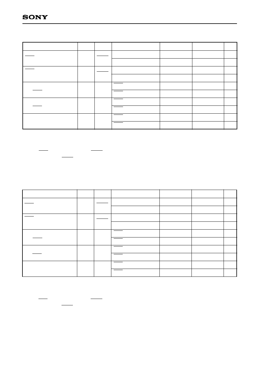
DC Characteristics (V
DD
= 2.7 to 3.3V)
Electrical Characteristics
(Ta = ≠20 to +75∞C, V
SS
= 0V reference)
V
DD
= 2.7V, I
OL
= 4.5mA
V
DD
= 3.3V, V
IH
= 3.3V
V
DD
= 3.3V, V
IL
= 0.3V
V
DD
= 3.3V, V
IL
= 3.3V
V
DD
= 3.3V, V
IL
= 0.4V
V
DD
= 3.3V, V
IL
= 0.3V
V
DD
= 3.3V, V
IL
= 2.7V
V
DD
= 3.3V
V
I
= 0, 3.3V
V
DD
= 3.3V
V
OH
= 12V
High level
output voltage
Low level
output voltage
Input current
I/O leakage
current
0.3
≠0.3
0.1
≠0.1
≠0.9
≠1.0
V
V
V
V
V
µA
µA
µA
µA
µA
µA
µA
µA
µA
PD, PH
PA to PD,
PE2 to PE7,
PF to PG,
PI to PJ,
PK3 to PK7
PB5, PB6
1
,
PG0
1
,
PI5, PI6
1
,
PK3, PK4
1
PA to PD,
PE2 to PE7,
PF to PG,
PI to PJ,
PK3 to PK7
EXTAL
TEX
RST
2
PA to PD
3
,
PF to PG
3
,
PI to PK
3
Item
Symbol
Pins
Conditions
Min.
PA to PD
3
,
PF to PG
3
,
PI to PK
3
,
PE,
AN0 to AN3
RST
2
PH
Typ.
0.9
20
≠20
10
≠10
≠200
≠20
±10
50
Max.
Unit
V
OH
V
OL
I
IHE
I
ILE
I
IHT
I
ILT
I
ILR
I
IL
I
IZ
Open drain
output leakage
current
(N-ch Tr off
state)
L
LOH
V
DD
= 2.7V, I
OH
= ≠0.24mA
V
DD
= 2.7V, I
OH
= ≠0.45mA
V
DD
= 2.7V, I
OH
= ≠0.12mA
2.5
2.1
2.5
2.1
0.25
0.4
V
V
V
DD
= 2.7V, I
OH
= ≠0.90mA
V
DD
= 2.7V, I
OL
= 1.0mA
V
DD
= 2.7V, I
OL
= 1.4mA
≠ 20 ≠
CXP7400P10
Supply
current
4
Item
Symbol
Pins
Conditions
Min.
12
30
mA
mA
µA
0.7
3.5
10
PA to PD,
PE0 to PE1,
PF to PG,
PI to PK,
AN0 to AN3,
EXTAL,
RST
Clock 1MHz
0V for all pins excluding measured
pins
V
DD
= 3.0V ± 0.3V
3
Sleep mode
V
DD
= 3.0V ± 0.3V
12MHz crystal oscillation
(C
1
= C
2
= 15pF)
V
DD
I
DDS1
I
DD1
I
DDS3
C
IN
Typ.
Max.
Unit
Stop mode
(Termination of EXTAL and TEX pins
crystal oscillation)
V
DD
= 3.0V ± 0.3V
Input
capacity
pF
20
10
1
This case applies that Port B buffer capability switching register (BUFB: 010F4h, bits 6 and 5 = "1, 1") and
Ports G/I/K buffer capability switching register (BUFG: 010F5h, bits 0, 3, 4, 5 and 6 = "1, 1, 1, 1, 1") are ON.
2
RST pin specifies the input current when the pull-up resistor is selected, and specifies the leakage current
when no resistor is selected.
3
PA to PD, PF to PG and PI to PK pins specify the input current when the pull-up resistor is selected, and
specify the leakage current when no resistor is selected.
4
When all output pins are open.
CXP7400P10
≠ 21 ≠
1
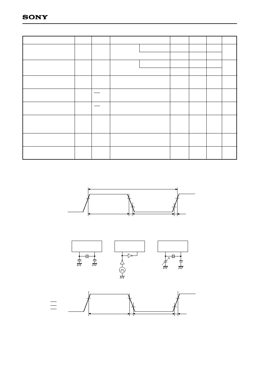
t
sys indicates three values according to the contents of the clock control register (CLC: 000FEh) upper 2
bits (CPU clock selection).
t
sys [ns] = 2000/fc (upper two bits = "00"), 4000/fc (upper two bits = "01"), 16000/fc (upper two bits = "11")
EXTAL
t
XH
t
XL
t
CF
t
CR
0.4V (V
DD
= 4.5 to 5.5V)
V
DD
≠ 0.4V (V
DD
= 4.5 to 5.5V)
1/fc
V
DD
≠ 0.2V
0.2V
Crystal oscillation
Ceramic oscillation
EXTAL
XTAL
External clock
EXTAL
XTAL
74HC04
C
1
C
2
32kHz clock applied conditions
Crystal oscillation
TEX
TX
C
1
C
2
TEX
EC0
EC1
EC2
t
EH
t
EL
t
EF
t
ER
0.2V
DD
0.8V
DD
t
TH
t
TL
t
TF
t
TR
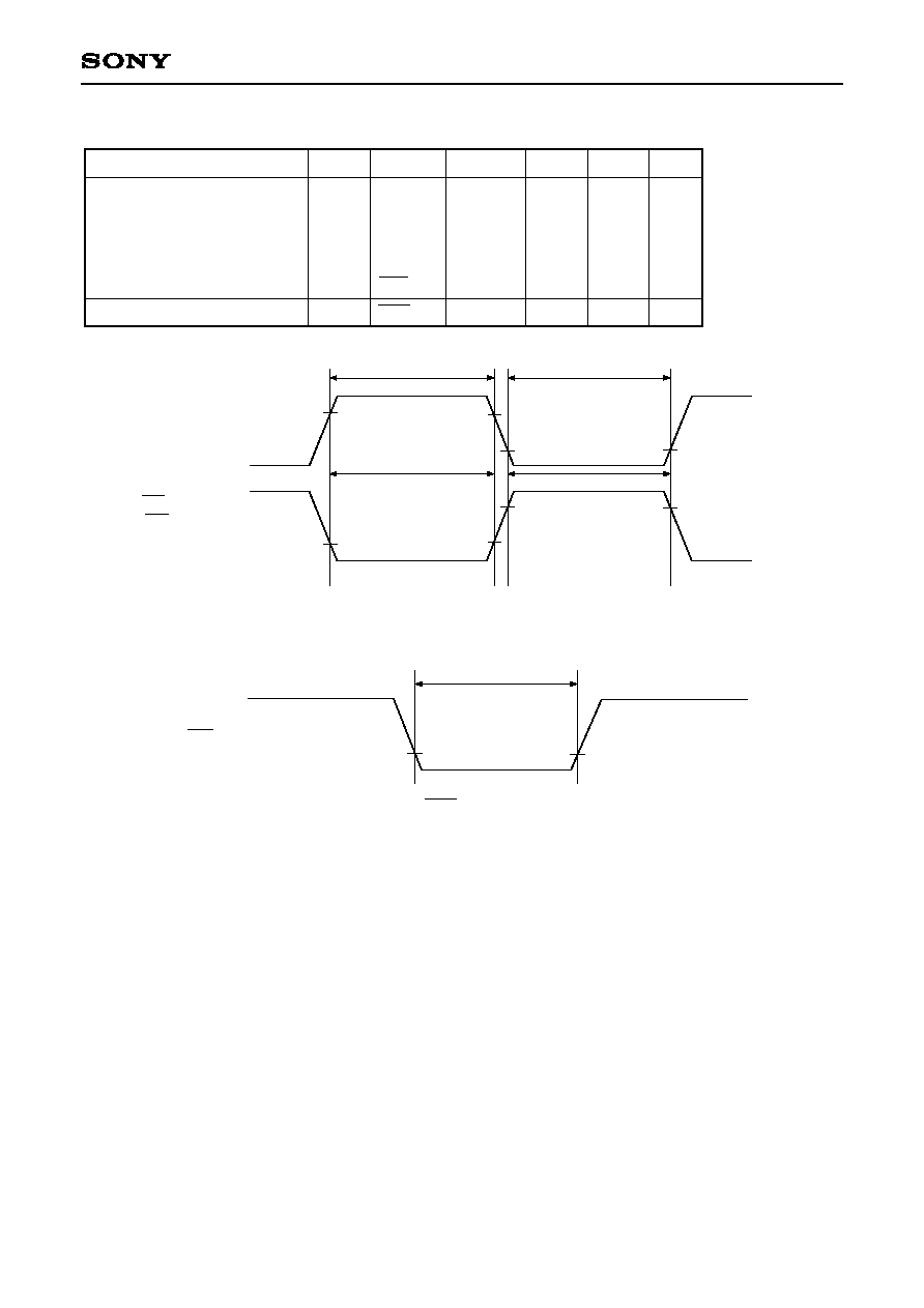
AC Characteristics
(1) Clock timing
System clock frequency
System clock input pulse
width
System clock input
rise time, fall time
Event count input clock
pulse width
Event count input clock
rise time, fall time
System clock frequency
Event count input clock
pulse width
Event count input clock
rise time, fall time
f
C
t
XL
,
t
XH
t
CR
,
t
CF
t
EH
,
t
EL
t
ER
,
t
EF
f
C
t
TL
,
t
TH
t
TR
,
t
TF
XTAL
EXTAL
EXTAL
EXTAL
EC
EC
TEX
TX
TEX
TEX
MHz
ns
ns
ns
ms
kHz
µs
ms
Item
Symbol
Pin
Conditions
Min.
Unit
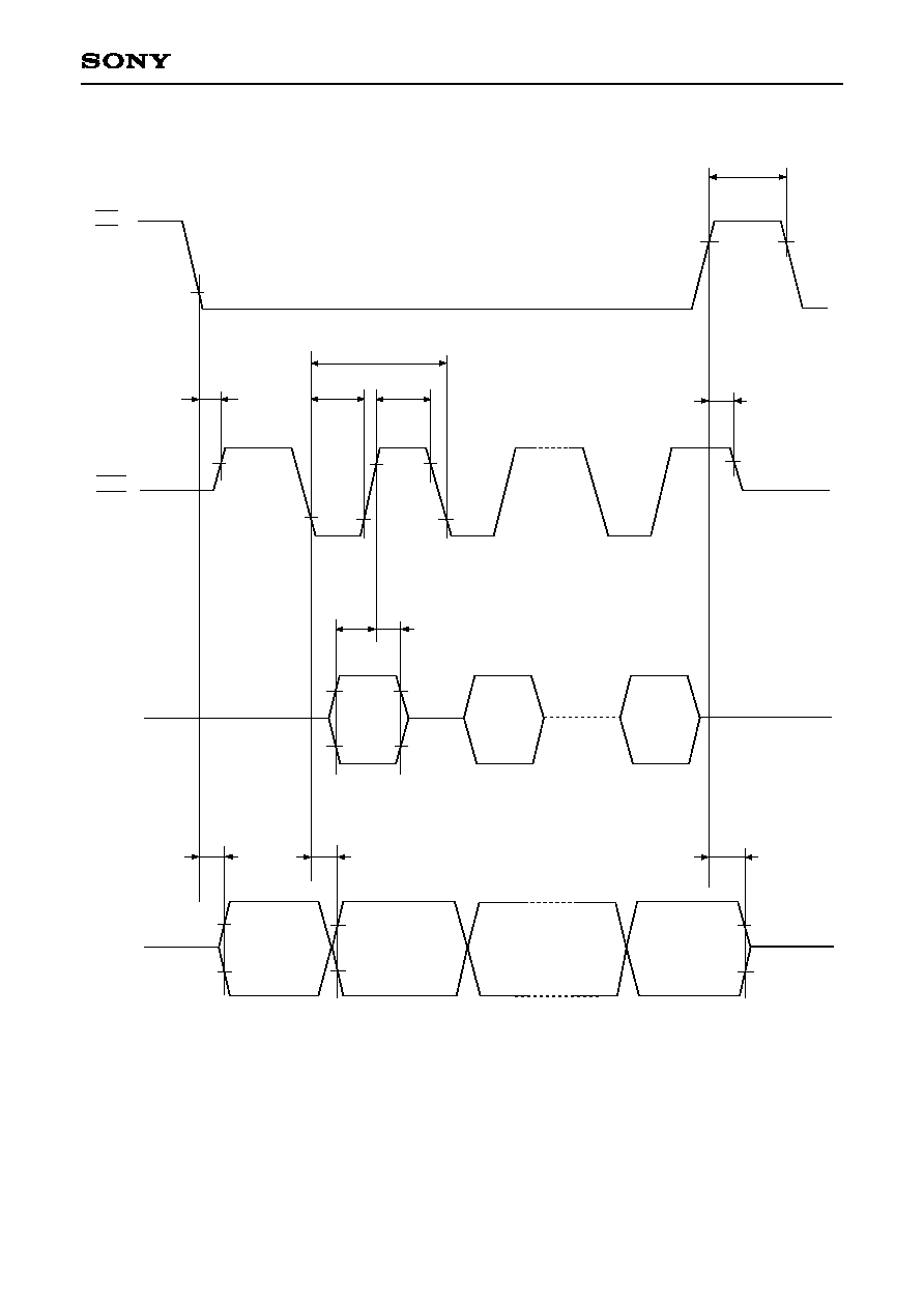
Fig. 1, Fig. 2
Fig. 1, Fig. 2
External clock drive
Fig. 1, Fig. 2
External clock drive
Fig. 3
Fig. 3
V
DD
= 2.7 to 5.5V
Fig. 2 (32kHz clock applied
condition)
Fig. 3
Fig. 3
1
1
28
37.5
t
sys + 50
1
10
Typ.
32.768
Max.
24
12
200
20
20
(Ta = ≠20 to +75∞C, V
DD
= 2.7 to 5.5V, Vss = 0V reference)
Fig. 2. Clock applied conditions
Fig. 1. Clock timing
Fig. 3. Event count clock timing
V
DD
= 4.5 to 5.5V
V
DD
= 4.5 to 5.5V
≠ 22 ≠
CXP7400P10
Note 1)
t
sys indicates three values according to the contents of the clock control register (CLC: 000FEh)
upper 2 bits (CPU clock selection).
t
sys [ns] = 2000/fc (upper 2 bits = "00"), 4000/fc (upper 2 bits = "01"), 16000/fc (upper 2 bits = "11")
Note 2) CS, SCK, SI and SO represent CS0, SCK0, SI0 and SO0 for CH0; they represent CS1, SCK1, SI1
and SO1 for CH1, respectively.
Note 3) The load of SCK output mode and SO output delay time is 50pF + 1TTL.
Note 4) This case applies that Port I/K output buffer capability switching register (BUFG: 010F5h, bits 6, 5, 4
and 3 = "0, 0, 0, 0") is OFF.
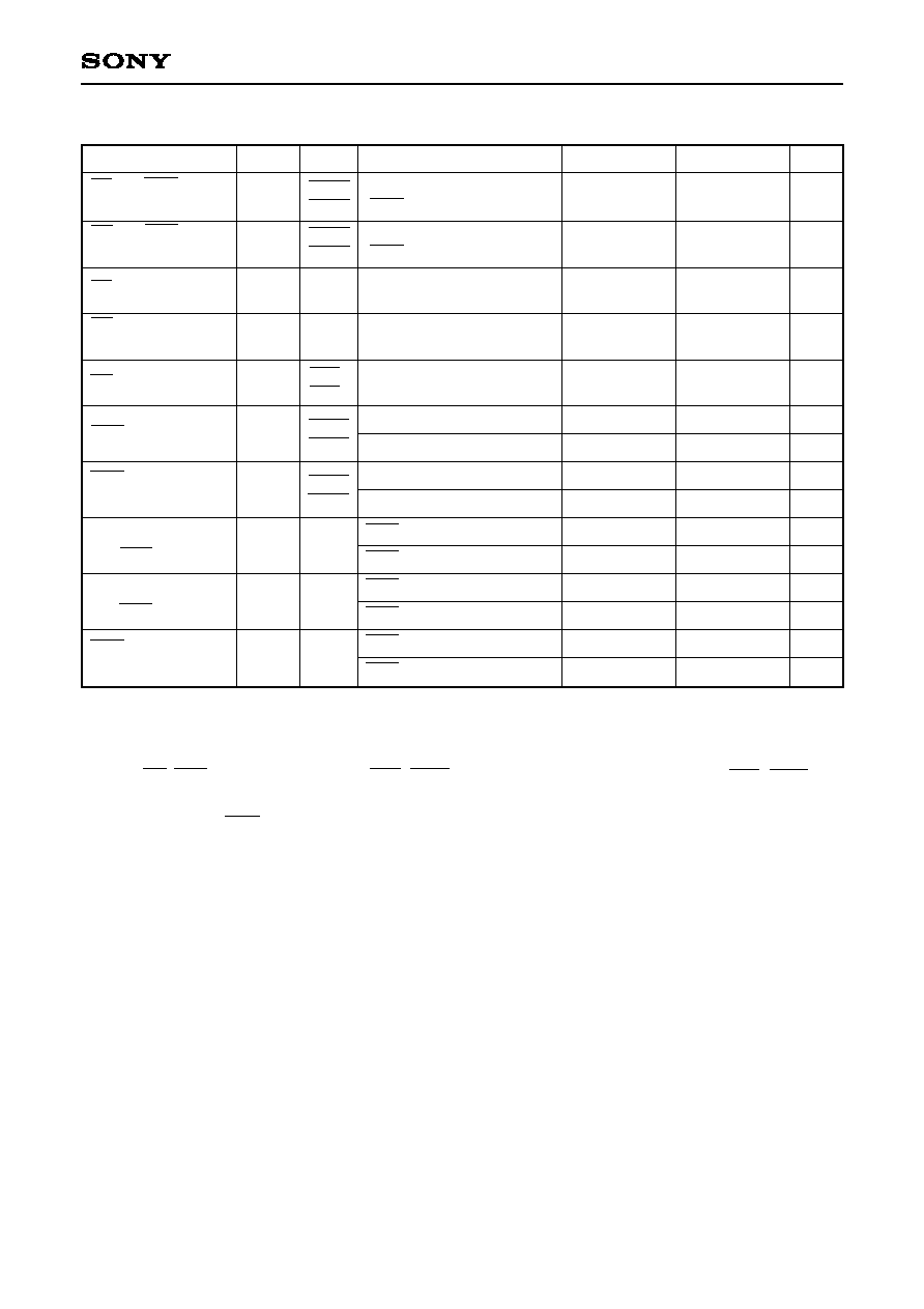
(2) Serial transfer (CH0, CH1)
(Ta = ≠20 to +75∞C, V
DD
= 4.5 to 5.5V, Vss = 0V reference)
CS
SCK
delay time
CS
SCK
floating delay time
CS
SO delay time
CS
SO floating
delay time
CS High level width
t
sys + 200
2
t
sys + 200
8000/fc
t
sys + 100
4000/fc ≠ 50
≠
t
sys + 100
200
2
t
sys + 200
100
1.5
t
sys + 200
1.5
t
sys + 200
1.5
t
sys + 200
1.5
t
sys + 200
2
t
sys + 200
100
ns
ns
ns
ns
ns
ns
ns
ns
ns
ns
ns
ns
ns
ns
ns
Item
Symbol
Pin
Conditions
Min.
Max.
Unit
Chip select transfer mode
(SCK = output mode)
Chip select transfer mode
(SCK = output mode)
Chip select transfer mode
Chip select transfer mode
Chip select transfer mode
Input mode
Output mode
Input mode
Output mode
SCK input mode
SCK output mode
SCK input mode
SCK output mode
SCK input mode
SCK output mode
SCK cycle time
SCK High and Low
level width
SI input setup time
(for SCK
)
SI input hold time
(for SCK
)
SCK
SO
delay time
t
DCSK
t
DCSKF
t
DCSO
t
DCSOF
t
WHCS
t
KCY
t
KH
t
KL
t
SIK
t
KSI
t
KSO
SCK0
SCK1
SCK0
SCK1
SO0
SO1
SO0
SO1
CS0
CS1
SCK0
SCK1
SCK0
SCK1
SI0
SI1
SI0
SI1
SO0
SO1
≠ 23 ≠
CXP7400P10
Note 1)
t
sys indicates three values according to the contents of the clock control register (CLC: 000FEh)
upper 2 bits (CPU clock selection).
t
sys [ns] = 2000/fc (upper 2 bits = "00"), 4000/fc (upper 2 bits = "01"), 16000/fc (upper 2 bits = "11")
Note 2) CS, SCK, SI and SO represent CS0, SCK0, SI0 and SO0 for CH0; they represent CS1, SCK1, SI1
and SO1 for CH1, respectively.
Note 3) The load of SCK output mode and SO output delay time is 50pF.
Note 4) This case applies that Port I/K output buffer capability switching register (BUFG: 010F5h, bits 6, 5, 4
and 3 = "1, 1, 1, 1") is ON.
Serial transfer (CH0, CH1)
(Ta = ≠20 to +75∞C, V
DD
= 2.7 to 3.3V, Vss = 0V reference)
CS
SCK
delay time
CS
SCK
floating delay time
CS
SO delay time
CS
SO floating
delay time
CS High level width
t
sys + 200
2
t
sys + 200
8000/fc
t
sys + 100
4000/fc ≠ 100
≠
t
sys + 100
200
2
t
sys + 200
100
1.5
t
sys + 250
1.5
t
sys + 250
1.5
t
sys + 250
1.5
t
sys + 250
2
t
sys + 250
125
ns
ns
ns
ns
ns
ns
ns
ns
ns
ns
ns
ns
ns
ns
ns
Item
Symbol
Pin
Conditions
Min.
Max.
Unit
Chip select transfer mode
(SCK = output mode)
Chip select transfer mode
(SCK = output mode)
Chip select transfer mode
Chip select transfer mode
Chip select transfer mode
Input mode
Output mode
Input mode
Output mode
SCK input mode
SCK output mode
SCK input mode
SCK output mode
SCK input mode
SCK output mode
SCK cycle time
SCK High and Low
level widths
SI input setup time
(for SCK
)
SI input hold time
(for SCK
)
SCK
SO
delay time
t
DCSK
t
DCSKF
t
DCSO
t
DCSOF
t
WHCS
t
KCY
t
KH
t
KL
t
SIK
t
KSI
t
KSO
SCK0
SCK1
SCK0
SCK1
SO0
SO1
SO0
SO1
CS0
CS1
SCK0
SCK1
SCK0
SCK1
SI0
SI1
SI0
SI1
SO0
SO1
≠ 24 ≠
CXP7400P10
CS0
CS1
SCK0
SCK1
0.2V
DD
0.8V
DD
t
WHCS
t
DCSK
t
DCSKF
0.8V
DD
0.2V
DD
0.8V
DD
t
KCY
t
KL
t
KH
0.8V
DD
0.2V
DD
SI0
SI1
t
SIK
t
KSI
Input data
t
DCSO
t
KSO
t
DCSOF
Output data
0.8V
DD
0.2V
DD
SO0
SO1
Fig. 4. Serial transfer CH0, CH1 timing
≠ 25 ≠
CXP7400P10
Serial transfer (CH2)
(Ta = ≠20 to +75∞C, V
DD
= 4.5 to 5.5V, Vss = 0V reference)
Item
Symbol
Pin
Min.
Max.
Unit
Conditions
SCK cycle time
SCK High and Low
level widths
SI input setup time
(for SCK
)
SI input hold time
(for SCK
)
SCK
SO delay time
t
KCY
t
KH
t
KL
t
SIK
t
KSI
t
KSO
SCK2
SCK2
SI2
SI2
SO2
Input mode
Output mode
Input mode
Output mode
SCK input mode
SCK output mode
SCK input mode
SCK output mode
SCK input mode
SCK output mode
1000
8000/fc
400
4000/fc ≠ 50
100
200
200
100
200
100
ns
ns
ns
ns
ns
ns
ns
ns
ns
ns
Note 1)
t
sys indicates three values according to the contents of the clock control register (CLC: 000FEh) upper
2 bits (CPU clock selection).
t
sys [ns] = 2000/fc (upper 2 bits = "00"), 4000/fc (upper 2 bits = "01"), 16000/fc (upper 2 bits = "11")
Note 2) SCK, SI and SO represent SCK2, SI2 and SO2 for CH2, respectively.
Note 3) The load of SCK2 output mode and SO2 output delay time is 50pF + 1TTL.
Note 4) This case applies that Port B output buffer capability switching register (BUFB: 010F4h, bits 6 and 5 =
"0, 0") is OFF.
Serial transfer (CH2)
(Ta = ≠20 to +75∞C, V
DD
= 2.7 to 3.3V, Vss = 0V reference)
Note 1)
t
sys indicates three values according to the contents of the clock control register (CLC: 000FEh) upper
2 bits (CPU clock selection).
t
sys [ns] = 2000/fc (upper 2 bits = "00"), 4000/fc (upper 2 bits = "01"), 16000/fc (upper 2 bits = "11")
Note 2) SCK, SI and SO represent SCK2, SI2 and SO2 for CH2, respectively.
Note 3) The load of SCK2 output mode and SO2 output delay time is 50pF.
Note 4) This case applies that Port B output buffer capability switching register (BUFB: 010F4h, bits 6 and 5 =
"1, 1") is ON.
Item
Symbol
Pin
Min.
Max.
Unit
Conditions
SCK cycle time
SCK High and Low
level widths
SI input setup time
(for SCK
)
SI input hold time
(for SCK
)
SCK
SO delay time
t
KCY
t
KH
t
KL
t
SIK
t
KSI
t
KSO
SCK2
SCK2
SI2
SI2
SO2
Input mode
Output mode
Input mode
Output mode
SCK input mode
SCK output mode
SCK input mode
SCK output mode
SCK input mode
SCK output mode
1000
8000/fc
400
4000/fc ≠ 100
100
200
200
100
250
125
ns
ns
ns
ns
ns
ns
ns
ns
ns
ns
≠ 26 ≠
CXP7400P10
Fig. 5. Serial transfer CH2 timing
t
KCY
t
KL
t
KH
0.2V
DD
0.8V
DD
t
SIK
t
KSI
t
KSO
Input data
Output data
0.2V
DD
0.8V
DD
0.2V
DD
0.8V
DD
SCK2
SI2
SO2
≠ 27 ≠
CXP7400P10
Analog input
Linearity error
V
FT
V
ZT
00h
01h
FEh
FFh
D
i
g
i
t
a
l
c
o
n
v
e
r
s
i
o
n
v
a
l
u
e
(3) A/D converter characteristics
(Ta = ≠20 to +75∞C, V
DD
= AV
DD
= 4.5 to 5.5V, AV
REF
= 4.0 to AV
DD
, Vss = AV
SS
= 0V reference)
Fig. 6. Definition of A/D converter terms
1
V
ZT
: Value at which the digital conversion value changes
from 00h to 01h and vice versa.
2
V
FT
: Value at which the digital conversion value changes
from FEh to FFh and vice versa.
3
f
ADC
indicates the below values due to the contents of bit
6 (CKS) of the A/D control register (ADC: 000F9h).
PS3 selected
f
ADC
= fc/4
PS4 selected
f
ADC
= fc/8
However, when PS3 is selected, fc is 12MHz or less.
4
Sub clock operated
t
CONV
= 34/f
TEX
t
SAMP
= 10/f
TEX
Resolution
Linearity errror
Absolute error
Conversion time
Sampling time
Reference input voltage
Analog input voltage
AV
REF
current
t
CONV
t
SAMP
V
REF
V
IAN
I
REF
I
REFS
AV
REF
AN0 to AN11
AV
REF
V
DD
= AV
DD
= 4.5 to 5.5V
Operation mode
Sleep mode
Stop mode
32kHz operation mode
Item
Symbol
Pin
Conditions
Min.
Typ.
Max.
Unit
Bits
LSB
LSB
µs
µs
V
V
mA
µA
8
±2
±3
1.0
10
0.6
31/f
ADC
3,
4
10/f
ADC
3,
4
AV
DD
≠ 0.5
0
Ta = 25∞C
V
DD
= AV
DD
= AV
REF
= 5.0V
V
SS
= AV
SS
= 0V
Resolution
Linearity errror
Absolute error
Conversion time
Sampling time
Reference input voltage
Analog input voltage
AV
REF
current
t
CONV
t
SAMP
V
REF
V
IAN
I
REF
I
REFS
AV
REF
AN0 to AN11
AV
REF
V
DD
= AV
DD
= 2.7 to 3.3V
Operation mode
Sleep mode
Stop mode
32kHz operation mode
Item
Symbol
Pin
Conditions
Min.
Typ.
Max.
Unit
Bits
LSB
LSB
µs
µs
V
V
mA
µA
(Ta = ≠20 to +75∞C, V
DD
= AV
DD
= 2.7 to 3.3V, AV
REF
= 2.7 to AV
DD
, Vss = AV
SS
= 0V reference)
8
±2
±3
0.7
10
0.4
31/f
ADC
3,
4
10/f
ADC
3,
4
AV
DD
≠ 0.3
0
Ta = 25∞C
V
DD
= AV
DD
= AV
REF
= 3.0V
V
SS
= AV
SS
= 0V
≠ 28 ≠
CXP7400P10
0.2V
DD
0.8V
DD
t
IH
t
IL
t
IL
t
IH
INT0
INT1
INT2
INT3
INT4
NMI
(NMI is specified only for
the falling edge)
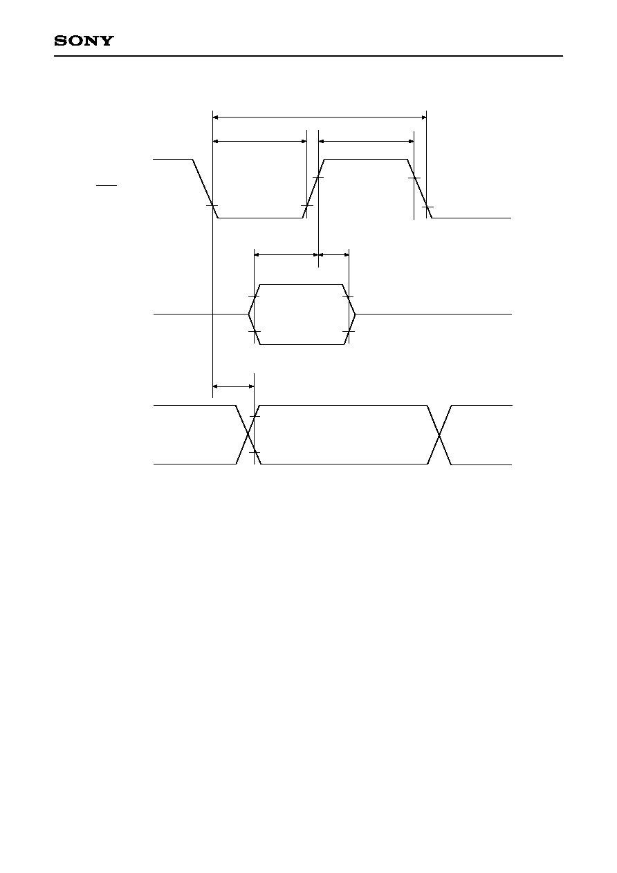
t
RSL
0.2V
DD
RST
External interruption
High and Low level widths
Reset input Low level width
INT0
INT1
INT2
INT3
INT4
NMI
RST
1
32/fc
µs
µs
Item
Symbol
Pin
Conditions
Min.
Max.
Unit
t
IH
t
IL
t
RSL
(4) Interruption, reset input
Fig. 7. Interruption input timing
Fig. 8. RST input timing
(Ta = ≠20 to +75∞C, V
DD
= 2.7 to 5.5V, Vss = 0V reference)
≠ 29 ≠
CXP7400P10
Appendix
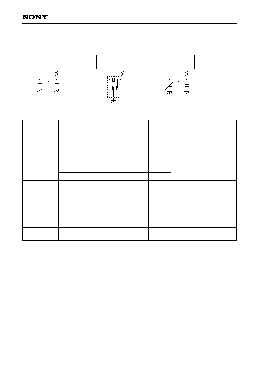
Fig. 9. Recommended oscillation circuit
C
2
Rd
EXTAL
XTAL
C
1
(i) Main clock
TEX
TX
C
1
C
2
Rd
(iii) Sub clock
Rd
EXTAL
XTAL
C
1
C
2
(ii) Main clock
Manufacturer
RIVER
ELETEC
CORPORATION
MURATA MFG
CO., LTD.
CSA10.0MTZ
CSA12.0MTZ
CSA16.00MXZ040
CST10.0MTW
CST12.0MTW
CST16.00MXW0C1
KINSEKI LTD.
Seiko
Instruments Inc.
Model
HC-49/U03
HC-49/U (-S)
VTC-200
SP-T
fc (MHz)
10.0
12.0
16.0
10.0
12.0
16.0
8.0
12.0
16.0
8.0
12.0
16.0
30
5
30
5
18
12
10
10
5
Open
18
30
5
30
5
18
12
10
10
5
Open
18
0
1
330
1
0
1
32.768kHz
330k
(iii)
C
1
(pF)
C
2
(pF)
Rd (
)
Circuit
example
(i)
Indicates types with on-chip grounding capacitor (C1, C2).
1
XTAL series resistor (Rd = 500
or less) is hard to affect noise by ESD.
(i)
(ii)
C
L
= 12.5pF
Remarks

≠ 30 ≠
CXP7400P10
Characteristics Curve
20
(100µA)
3
4
5
6
0.1
5.0
1.0
V
DD
≠ Supply voltage [V]
I
D
D
≠
S
u
p
p
l
y
c
u
r
r
e
n
t
[
m
A
]
I
DD
vs. V
DD
(fc = 24MHz, Ta = 25∞C, Typical)
2
0.05
(50µA)
0.01
(10µA)
0.5
10.0
20.0
1/16 dividing mode
1/4 dividing mode
Sleep mode
32kHz operation
mode
0
20
10
fc ≠ System clock [MHz]
I
D
D
≠
S
u
p
p
l
y
c
u
r
r
e
n
t
[
m
A
]
I
DD
vs. fc
(V
DD
= 5.0V, Ta = 25∞C, Typical)
10
30
1/2 dividing mode
32kHz sleep mode
24
1/2 dividing mode
1/16 dividing mode
Sleep mode
1/4 dividing mode
0
(100µA)
3
4
5
6
0.1
5.0
1.0
V
DD
≠ Supply voltage [V]
I
D
D
≠
S
u
p
p
l
y
c
u
r
r
e
n
t
[
m
A
]
I
DD
vs. V
DD
(fc = 12MHz, Ta = 25∞C, Typical)
2
0.05
(50µA)
0.01
(10µA)
0.5
10.0
20.0
1/16 dividing mode
1/4 dividing mode
Sleep mode
1/2 dividing mode
20
0
20
10
fc ≠ System clock [MHz]
I
D
D
≠
S
u
p
p
l
y
c
u
r
r
e
n
t
[
m
A
]
I
DD
vs. fc
(V
DD
= 3.0V, Ta = 25∞C, Typical)
10
30
24
1/2 dividing mode
1/16 dividing mode
Sleep mode
1/4 dividing mode
0
40
40
50.0
50.0
≠ 31 ≠
CXP7400P10
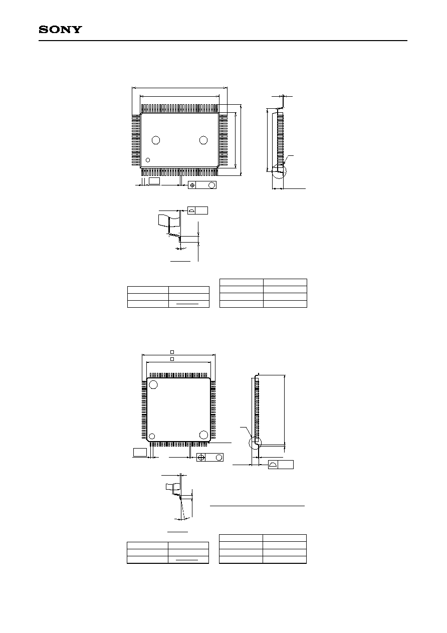
Package Outline
Unit: mm
SONY CODE
EIAJ CODE
JEDEC CODE
PACKAGE MATERIAL
LEAD TREATMENT
LEAD MATERIAL
PACKAGE MASS
EPOXY RESIN
SOLDER PLATING
42/COPPER ALLOY
PACKAGE STRUCTURE
23.9 ± 0.4
QFP-100P-L01
100PIN QFP (PLASTIC)
20.0 ≠ 0.1
+ 0.4
0.15 ≠ 0.05
+ 0.1
1
5
.
8
±
0
.
4
1
7
.
9
±
0
.
4
1
4
.
0
≠
0
.
1
+
0
.
4
2.75 ≠ 0.15
+ 0.35
A
0.65
M
0.13
QFP100-P-1420
1.7g
1
100
81
80
51
50
31
30
0.3 ≠ 0.1
+ 0.15
DETAIL A
0∞ to 10∞
0
.
8
±
0
.
2
(
1
6
.
3
)
0.15
0.1 ≠ 0.05
+ 0.2
SONY CODE
EIAJ CODE
JEDEC CODE
PACKAGE MATERIAL
LEAD TREATMENT
LEAD MATERIAL
PACKAGE MASS
EPOXY RESIN
SOLDER PLATING
42 ALLOY
PACKAGE STRUCTURE
DETAIL A
LQFP-100P-L01
LQFP100-P-1414
100PIN LQFP (PLASTIC)
16.0 ± 0.2
14.0 ± 0.1
75
51
50
26
25
1
76
0.5
0.18 ≠ 0.03
+ 0.08
(0.22)
A
1.5 ≠ 0.1
+ 0.2
0.127 ≠ 0.02
+ 0.05
0
.
5
±
0
.
2
(
1
5
.
0
)
0∞ to 10∞
0.1 ± 0.1
0
.
5
±
0
.
2
100
0.1
NOTE: Dimension "
" does not include mold protrusion.
0.8g
0.13 M