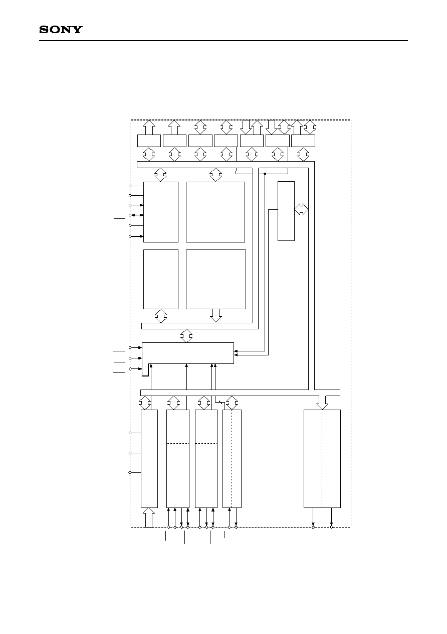
Description
The CXP81120/81124 is a CMOS 8-bit micro-
computer which consists of A/D converter, serial
interface, timer/counter, time base timer, PWM
output, as well as basic configurations like 8-bit
CPU, ROM, RAM and I/O port. They are integrated
into a single chip.
Also the CXP81120/81124 provides power-on reset
function, sleep/stop function which enables to lower
power consumption.
Features
∑ A wide instruction set (213 instructions) which covers various types of data
-- 16-bit operation/multiplication and division/Boolean bit operation instructions
∑ Minimum instruction cycle
250ns at 16MHz operation (4.5 to 5.5V)
333ns at 12MHz operation (3.0 to 5.5V)
∑ Incorporated ROM capacity
20K bytes (CXP81120)
24K bytes (CXP81124)
∑ Incorporated RAM capacity
832 bytes
∑ Peripheral functions
-- A/D converter
8-bit, 8-channel, successive approximation system
(Conversion time: 20µs at 16MHz)
-- Serial interface
Incorporated buffer RAM (1 to 32 bytes auto transfer), 1 channel
Incorporated 8-bit and 8-stage FIFO
(1 to 8 bytes auto transfer), 1 channel
-- Timer
8-bit timer, 8-bit timer/counter, 19-bit time base timer
-- PWM output
12 bits, 2 channels
∑ Interruption
10 factors, 10 vectors, multi-interruption possible
∑ Standby mode
Sleep/stop
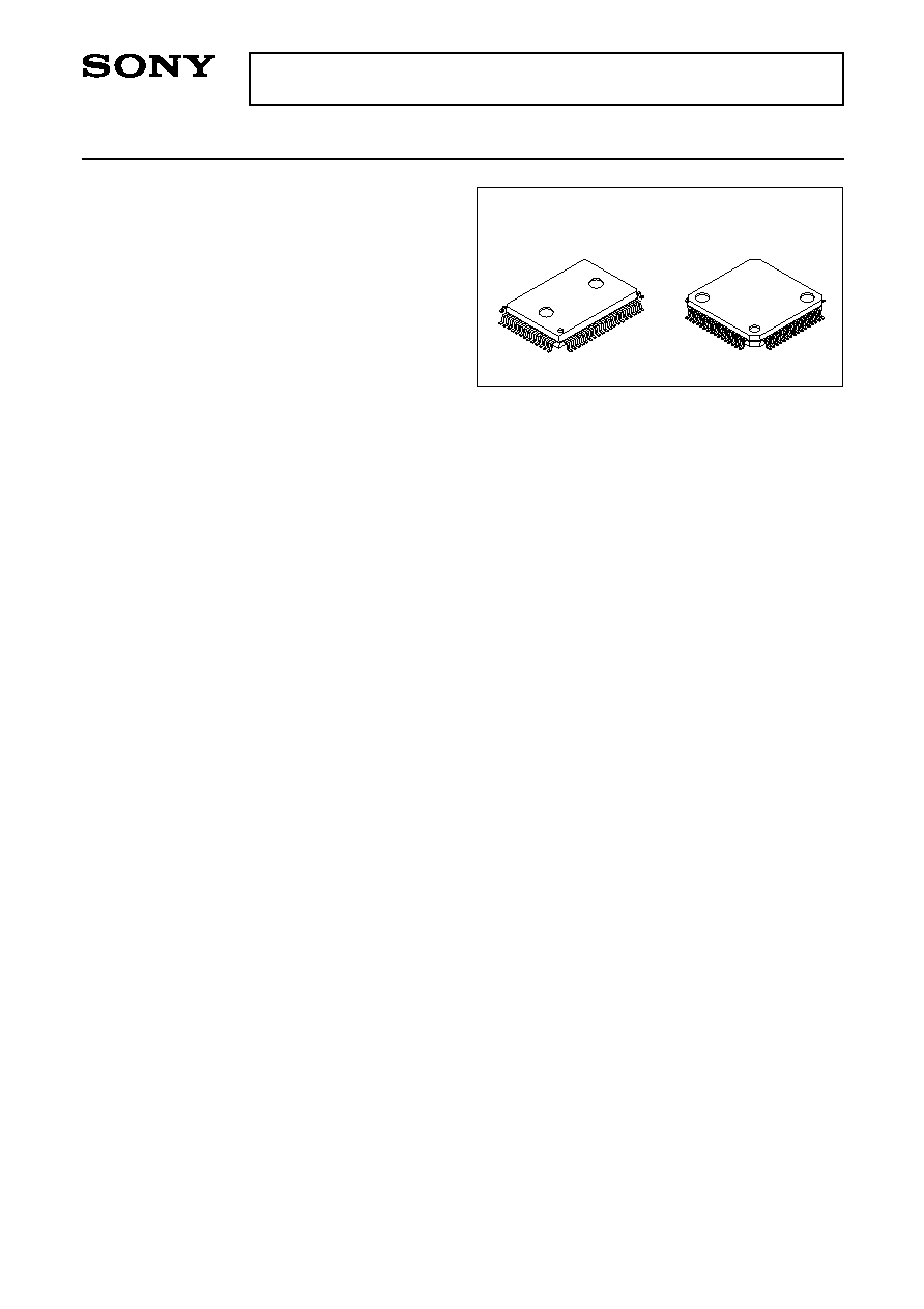
∑ Package
64-pin plastic QFP/LQFP
∑ Piggyback/evaluator
CXP81100 64-pin ceramic PQFP
Structure
Silicon gate CMOS IC
≠ 1 ≠
CXP81120/81124
E94414B16-PS
CMOS 8-bit Single Chip Microcomputer
Sony reserves the right to change products and specifications without prior notice. This information does not convey any license by
any implication or otherwise under any patents or other right. Application circuits shown, if any, are typical examples illustrating the
operation of the devices. Sony cannot assume responsibility for any problems arising out of the use of these circuits.
64 pin LQFP (Plastic)
64 pin QFP (Plastic)
≠ 3 ≠
CXP81120/81124
17
18
19
20 21 22 23 24 25 26 27 28 29 30 31 32
40
39
38
37
36
35
34
33
41
42
43
44
45
46
47
48
2
3
4
5
6
7
8
9
11
12
13
14
15
16
1
10
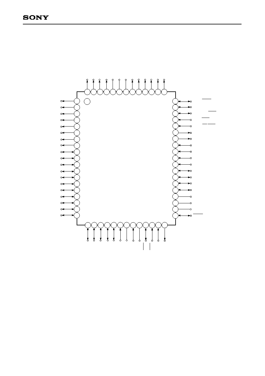
PB7
PB6
PB5
PB4
PB3
PB2
PB1
PB0
PC7
PC6
PC5
PC4
PC3
PC2
PC1
PC0
PG6/SO1
PG7/SI1/INT1
PE0/INT0
PE1/EC/INT2
PE2/PWM0
PE3/PWM1
PF0/AN0
PF1/AN1
PF2/AN2
PF3/AN3
PF4/AN4
PF5/AN5
PF6/AN6
PF7/AN7
AV
DD
AV
REF
PA0
PA1
PA2
PA3
V
SS
V
DD
NC
PA4
PA5
PA6
PA7
PG3/TO
PG4
PG5/SCK1
PD4
PD3
PD2
PD1
PD0
MP
XTAL
EXTAL
V
SS
RST
CS0
SI0
SO0
SCK0
AV
SS
49
50
51
52
53
54
55
56
57
58
59
60
63
64
61
62
PD7
PD6
PD5
Pin Configuration (Top View) 64-pin QFP
Note) 1.
NC (Pin 58) is always connected to V
DD
.
2.
Vss (Pins 28 and 60) are both connected to GND.
3.
MP (Pin 25) is always connected to GND.
≠ 4 ≠
CXP81120/81124
17 18 19 20 21 22 23 24 25 26 27 28 29 30
40
39
38
37
36
35
34
31 32
33
41
42
43
44
45
46
47
48
2
3
4
5
6
7
8
9
11
12
13
14
15
16
1
10
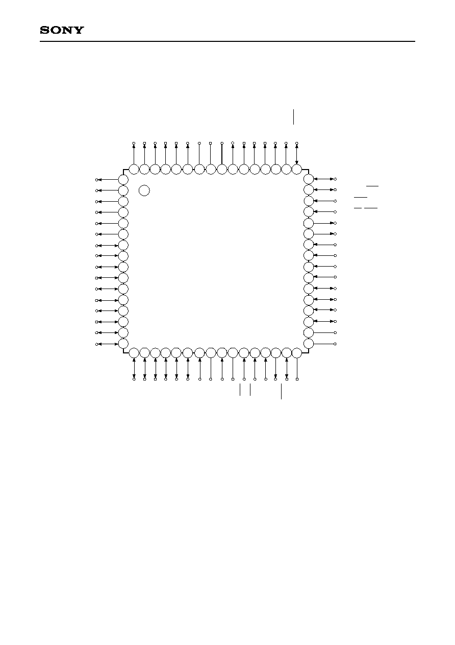
PB5
PB4
PB3
PB2
PB1
PB0
PC7
PC6
PC5
PC4
PC3
PC2
PC1
PC0
PD7
PD6
PG6/SO1
PG7/SI1/INT1
PE0/INT0
PE1/EC/INT2
PE2/PWM0
PE3/PWM1
PF0/AN0
PF1/AN1
PF2/AN2
PF3/AN3
PF4/AN4
PF5/AN5
PF6/AN6
PF7/AN7
AV
DD
AV
REF
PB6
PB7
PA0
PA1
PA2
PA3
V
SS
V
DD
NC
PA4
PA5
PA6
PA7
PG3/TO
PG4
PG5/SCK1
PD5
PD4
PD3
PD2
PD1
PD0
MP
XTAL
EXTAL
V
SS
RST
CS0
SI0
SO0
SCK0
AV
SS
49
50
51
52
53
54
55
56
57
58
59
60
63
64
61
62
Pin Configuration (Top View) 64-pin LQFP
Note) 1.
NC (Pin 56) is always connected to V
DD
.
2.
Vss (Pins 26 and 58) are both connected to GND.
3.
MP (Pin 23) is always connected to GND.
≠ 5 ≠
CXP81120/81124
(Port A)
8-bit output port.
(8 pins)
(Port B)
8-bit output port.
(8 pins)
(Port C)
8-bit I/O port. I/O can be set in a unit of single bits.
(8 pins)
(Port D)
8-bit I/O port. I/O and function as standby release input can be set in a unit of
single bits.
(8 pins)
(Port E)
4-bit port. Lower 2 bits
are for input; upper 2 bits
are for output.
(4 pins)
(Port F)
8-bit port. Lower 4 bits are for input; upper
4 bits are for output.
Lower 4 bits also serve as standby release
input.
(8 pins)
Serial clock (CH0) I/O.
Serial data (CH0) output.
Serial data (CH0) input.
Serial interface (CH0) chip select input.
(Port G)
5-bit port. Lower 2 bits
are for output; upper
3 bits are for I/O.
I/O can be set in a unit
of single bits.
(5 pins)
Connects a crystal oscillator for system clock. When supplying the external
clock, input the external clock to EXTAL pin and input opposite phase
clock to XTAL pin.
System reset; active at Low level. RST pin is I/O pin, which outputs "Low"
level by incorporated power-on reset function when power turns on.
(Mask option)
Pin Description
Symbol
PA0 to PA7
PB0 to PB7
PC0 to PC7
PD0 to PD7
PE0/INT0
PE1/EC/INT2
PE2/PWM0
PE3/PWM1
PF0/AN0
to
PF3/AN3
PF4/AN4
to
PF7/AN7
SCK0
SO0
SI0
CS0
PG3/TO
PG4
PG5/SCK1
PG6/SO1
PG7/SI1/INT1
EXTAL
XTAL
RST
Output
Output
I/O
I/O
Input/Input
Input/Input/
Input
Output/Output
Output/Output
Input/Input
Output/Input
I/O
Output
Input
Input
Output/Output
Output
I/O/I/O
I/O/Output
I/O/Input
Input
Input
Output
I/O
I/O
Description
Input to request external interruption.
Active at the falling edge. (2 pins)
External event
input for
timer/counter.
12-bit PWM output. (2 pins)
Analog input to A/D
converter.
(8 pins)
Serial data (CH1)
input.
Timer/counter rectangular wave output.
Serial clock (CH1) I/O.
Serial data (CH1) output.
Input to request external
interruption. Active at the
falling edge.