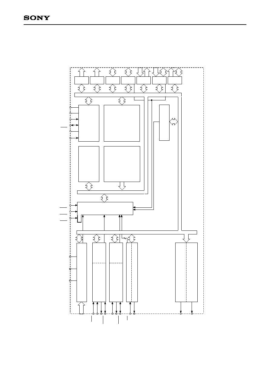
Description
The CXP811P24 is a CMOS 8-bit microcomputer
which consists of A/D converter, serial interface,
timer/counter, time base timer, PWM output, as well
as basic configurations like 8-bit CPU, PROM, RAM
and I/O port. They are integrated into a single chip.
Also the CXP811P24 provides power-on reset
function, sleep/stop function which enables to lower
power consumption .
The CXP811P24 is the PROM-incorporated version
of the CXP81120/81124 with built-in mask ROM.
This provides the additional feature of being able to
write directly into the program. Thus, it is most suitable
for evaluation use during system development and
for small-quantity production.
Features
∑ A wide instruction set (213 instructions) which covers various types of data
-- 16-bit operation/multiplication and division/Boolean bit operation instructions
∑ Minimum instruction cycle
250ns at 16MHz (4.5 to 5.5V)
333ns at 12MHz (3.0 to 5.5V)
∑ Incorporated PROM capacity
24K bytes
∑ Incorporated RAM capacity
832 bytes
∑ Peripheral functions
-- A/D converter
8-bit, 8-channel, successive approximation system
(Conversion time: 20µs at 16MHz)
-- Serial interface
Incorporated buffer RAM (1 to 32 bytes auto transfer), 1 channel
Incorporated 8-bit and 8-stage FIFO
(1 to 8 bytes auto transfer), 1 channel
-- Timer
8-bit timer, 8-bit timer/counter, 19-bit time base timer
-- PWM output
12 bits, 2 channels
∑ Interruption
10 factors, 10 vectors, multi-interruption possible
∑ Standby mode
Sleep/stop
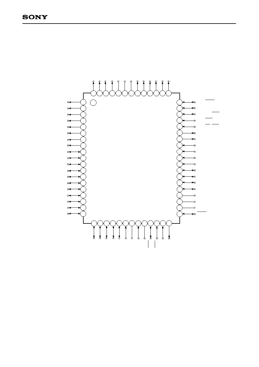
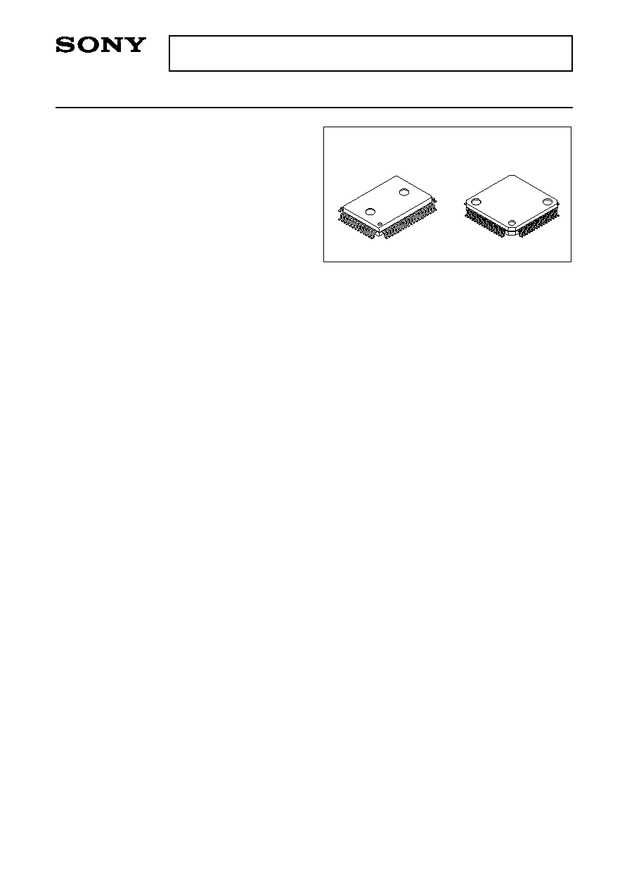
∑ Package
64-pin plastic QFP/LQFP
Structure
Silicon gate CMOS IC
≠ 1 ≠
CXP811P24
E94X40C18-PS
CMOS 8-bit Single Chip Microcomputer
Sony reserves the right to change products and specifications without prior notice. This information does not convey any license by
any implication or otherwise under any patents or other right. Application circuits shown, if any, are typical examples illustrating the
operation of the devices. Sony cannot assume responsibility for any problems arising out of the use of these circuits.
64 pin LQFP (Plastic)
64 pin QFP (Plastic)
(Port A)
8-bit output port.
(8 pins)
(Port B)
8-bit output port.
(8 pins)
(Port C)
8-bit I/O port. I/O can be set in a unit of single bits.
(8 pins)
(Port D)
8-bit I/O port. I/O and function as standby release input can be set in a unit
of single bits.
(8 pins)
(Port E)
4-bit port.
Lower 2 bits are for input;
upper 2 bits are for
output.
(4 pins)
(Port F)
8-bit port. Lower 4 bits are for input; upper
4 bits are for output.
Lower 4 bits also serve as standby release
input.
(8 pins)
Serial clock (CH0) I/O.
Serial data (CH0) output.
Serial data (CH0) input.
Serial intreface (CH0) chip select input.
(Port G)
5-bit port. Lower 2 bits
are for output; upper
3 bits are for I/O.
I/O port can be set in a
unit of single bits.
(5 pins)
Connects a crystal oscillator for system clock. When supplying the
external clock, input the external clock to EXTAL pin and input opposite
phase clock to XTAL pin.
System reset; active at Low level. RST pin is I/O pin, which outputs Low level
by incorporated power-on reset function when power turns on.
Analog input to A/D
converter. (8 pins)
External event
input for
timer/counter.
12-bit PWM output. (2 pins)
Input to request external interruption.
Active at the falling edge. (2 pins)
≠ 5 ≠
CXP811P24
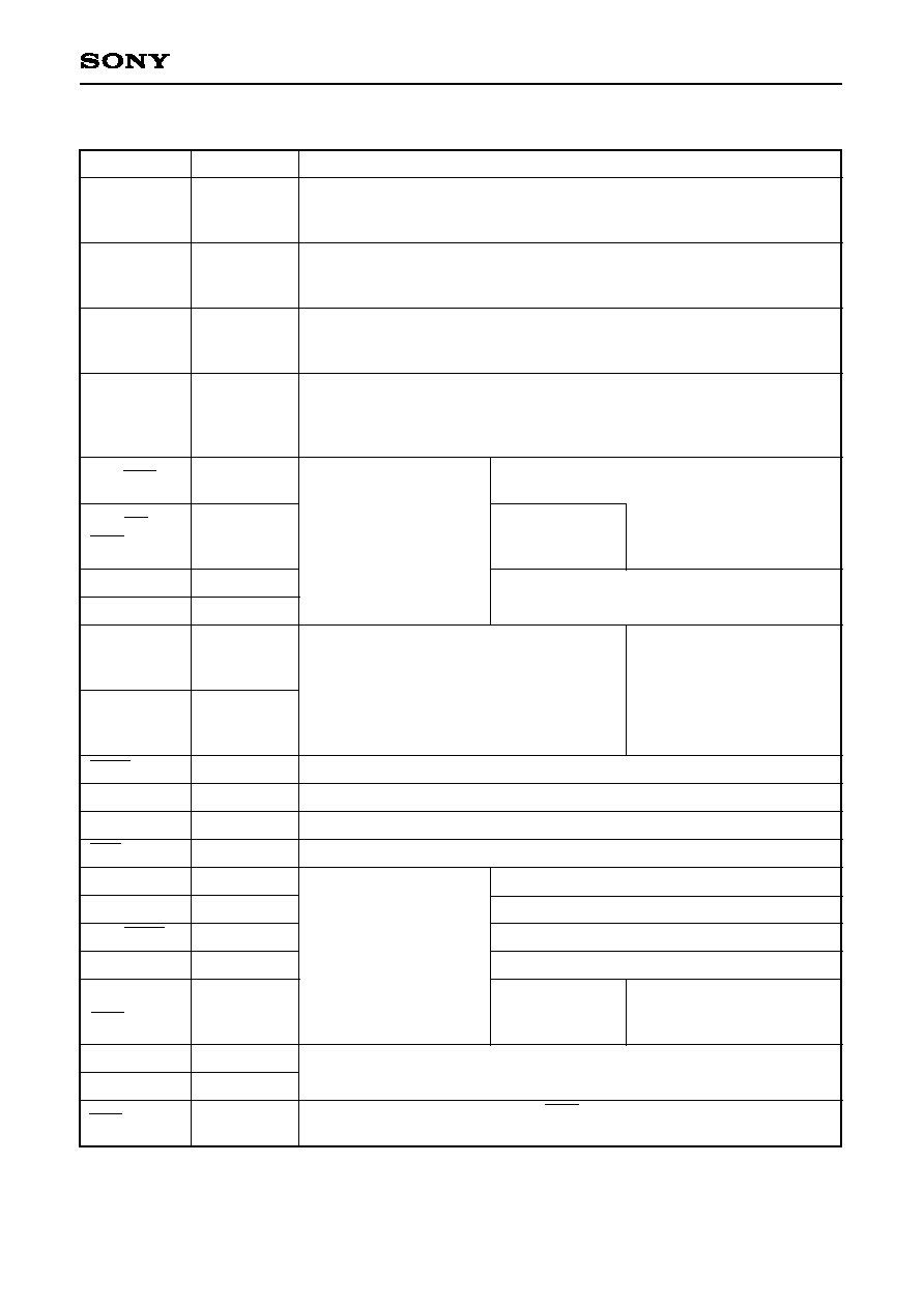
Pin Description
Symbol
PA0 to PA7
PB0 to PB7
PC0 to PC7
PD0 to PD7
PE0/INT0
PE1/EC/
INT2
PE2/PWM0
PE3/PWM1
PF0/AN0
to
PF3/AN3
PF4/AN4
to
PF7/AN7
SCK0
SO0
SI0
CS0
PG3/TO
PG4
PG5/SCK1
PG6/SO1
PG7/SI1/
INT1
EXTAL
XTAL
RST
Output
Output
I/O
I/O
Input/Input
Input/Input/
Input
Output/Output
Output/Output
Input/Input
Output/Input
I/O
Output
Input
Input
Output/Output
Output
I/O/I/O
I/O/Output
I/O/Input/
Input
Input
Output
I/O
I/O
Description
Serial data (CH1)
input.
Timer/counter rectangular wave output.
Serial clock (CH1) I/O.
Serial data (CH1) output.
Input to request external
interruption. Active at the
falling edge.