 | –≠–ª–µ–∫—Ç—Ä–æ–Ω–Ω—ã–π –∫–æ–º–ø–æ–Ω–µ–Ω—Ç: CXP823P24 | –°–∫–∞—á–∞—Ç—å:  PDF PDF  ZIP ZIP |
CMOS 8-bit Single Chip Microcomputer
Description
The CXP823P24 is a highly integrated CMOS 8-bit
single-chip microcomputer which is mainly composed
of an 8-bit CPU, PROM, RAM and I/O ports. This
microcomputer features many other high-performance
circuits in a single-chip CMOS design, including an
A/D converter, serial interface, timer/counter, time-
base timer, capture timer/counter, fluorescent display
tube controller/driver, and remote control receiver.
Also, the CXP823P24 provides the power-on reset
function as well as the sleep/stop function which
assures reduced power consumption.
Being a PROM-incorporated version of the
CXP82324 which has on-chip mask ROM, the
CXP823P24 permits program writing. Therefore, it is
ideally suited for use in system development stage
evaluation and job lot production.
Features
∑ Instruction set which supports a wide array of data types 213 types
-- 16-bit arithmetic instruction/multiplication and division instructions/boolean bit operation instruction
∑ Minimum instruction cycle
During operation 400ns/10MHz
∑ Incorporated PROM capacity 24K bytes
∑ Incorporated RAM capacity
704 bytes (Including fluorescent display data area)
∑ Peripheral functions
-- A/D converter
8-bit, 8-channel, successive comparison type
(conversion time: 32µs at 10MHz)
-- Serial interface
1 channel data interface with an 8-bit, 8-stage FIFO
(1 to 8 byte automatic transfer)
1-channel, 8-bit clock synchronized interface
-- Timers
8-bit timer
8-bit timer/counter
19-bit time-base timer
16-bit capture timer/counter
-- Fluorescent display tube controller/driver
Display of up to 336 segments
1 to 16 digit dynamic display
Dimmer function
High voltage tolerance output (40V)
Built-in pull-down resistor
-- Remote control receiver
Built-in noise suppressor circuit
Built-in 8-bit pulse counter and 6-stage FIFO
∑ Interrupts
14 factors, 15 vectors, multiple interrupt pocessing
∑ Standby mode
Sleep/stop
∑ Package
80-pin plastic QFP
≠ 1 ≠
E92Y35A78-PS
Sony reserves the right to change products and specifications without prior notice. This information does not convey any license by
any implication or otherwise under any patents or other right. Application circuits shown, if any, are typical examples illustrating the
operation of the devices. Sony cannot assume responsibility for any problems arising out of the use of these circuits.
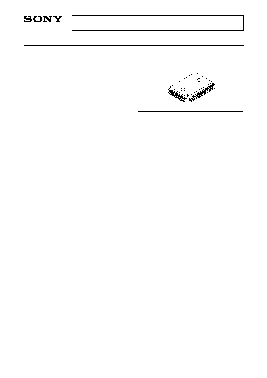
CXP823P24
80 pin QFP (Plastic)
Structure
Silicon gate CMOS IC
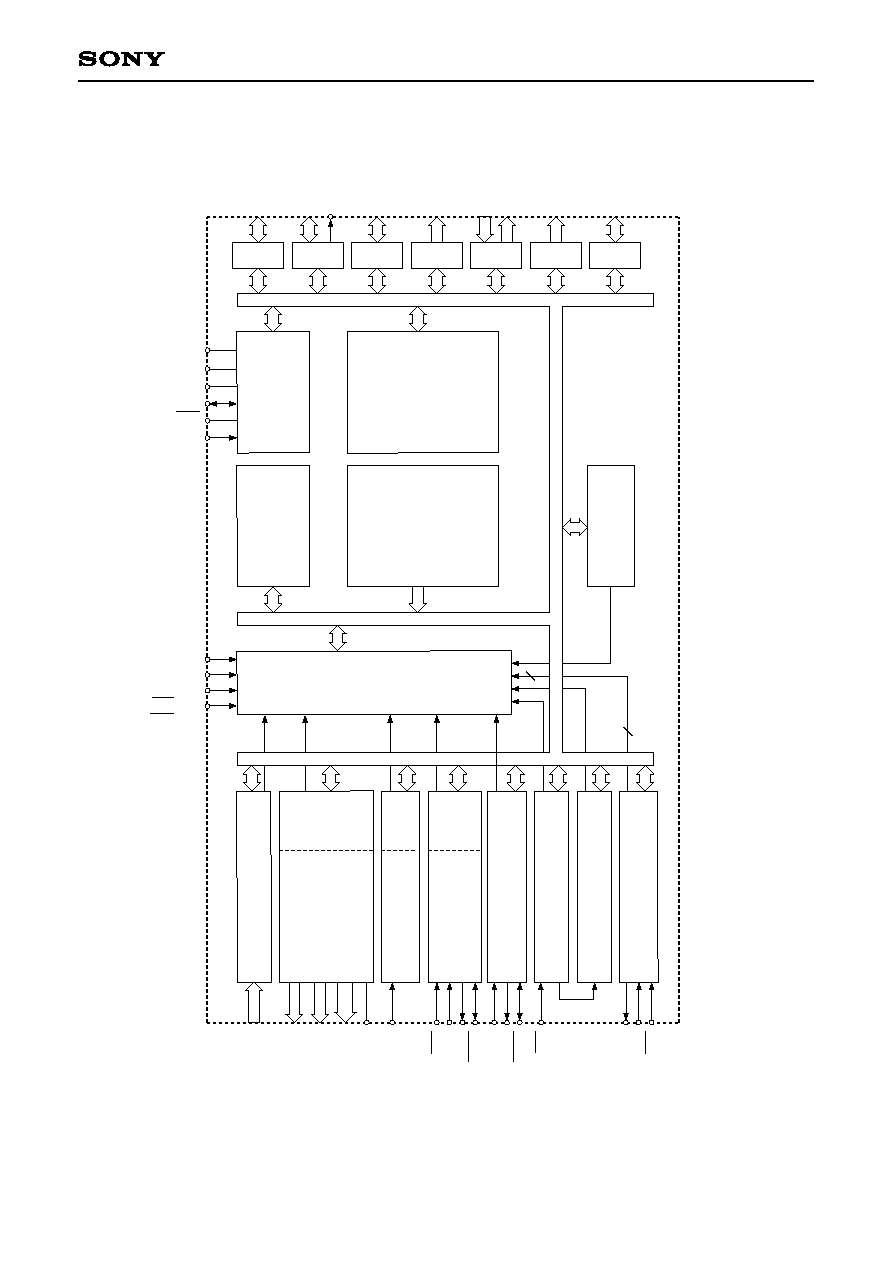
≠ 2 ≠
CXP823P24
PE0/EC0/INT0
PA0/AN0 to
PA7/AN7
T0 to T7
T8/S28 to
T15/S21
S0 to S20
V
FDP
PE4/RMC
PB1/CS0
PB3/SI0
PB0/SO0
PB2/SCK0
PE0/INT0/EC0
PE7/TO
PB0/CINT
PE1/INT1/EC1
A/D CONVERTER
FDP
CONTROLLER/
DRIVER
REMOCON
8 BIT TIMER/COUNTER 0
8 BIT TIMER 1
16 BIT CAPTURE
TIMER/COUNTER 2
RAM
80 BYTES
FIFO
SERIAL
INTERFACE
UNIT 0
FIFO
INTERRUPT CONTROLLER
SPC700
CPU CORE
PROM
24K BYTES
CLOCK
GENERATOR/
SYSTEM CONTROL
RAM
704 BYTES
2
2
PRESCALER/
TIME BASE TIMER
8
8
8
21
PE1/EC1/INT1
PE2/INT2
PE3/INT3
V
SS
PORT A
PORT B
PORT C
PORT D
PORT E
PORT F
PORT G
4
8
8
7
8
6
2
PA0 to PA7
PB0 to PB6
PC0 to PC7
PD0 to PD7
PE0 to PE5
PE6 to PE7
PF0 to PF7
PG0 to PG3
PB6/SI1
PB7/SO1
PB5/SCK1
SERIAL INTERFACE UNIT 1
8
V
DD
RST
XTAL
EXTAL
PB7
Vpp
Block Diagram
≠ 3 ≠
CXP823P24
PE3/INT3
PE4/RMC
PE5
PE6
PE7/TO
PB0/CINT
PB1/CS0
PB2/SCK0
PB3/SI0
PB4/SO0
PB5/SCK1
PB6/SI1
PB7/SO1
PC0/KR0
PC1/KR1
PC2/KR2
PC3/KR3
PC4/KR4
PC5/KR5
PC6/KR6
PC7/KR7
PA0/AN0
PA1/AN1
PA2/AN2
T7
T8/S28
T9/S27
T10/S26
T14/S22
T15/S21
S20
S19
S18
S17
S16
PF5/S13
PF4/S12
PF3/S11
PF2/S10
PF1/S9
PF0/S8
PD7/S7
PA3/AN3
PA4/AN4
PA5/AN5
RST
EXTAL
XTAL
V
SS
PD0/S0
PD1/S1
PD2/S2
Vpp
PE2/IN2
PG2
PG1
PG0
V
DD
V
FDP
T0
T1
T2
T3
T4
T5
34
31 32 33
41
42
43
44
45
46
47
48
49
50
51
52
53
54
55
56
57
58
59
60
70 69 68 67
63
64
65
66
61
62
71
73
74
75
76
77
78
79
80
2
3
4
5
6
7
8
9
10
11
12
14
15
16
17
18
19
20
21
22
23
24
25 26 27 28 29 30
1
T12/S24
T13/S23
T11/S25
PA6/AN6
PA7/AN7
40
39
38
37
36
35
PD3/S3
PD4/S4
PD5/S5
PD6/S6
PF7/S15
PF6/S14
T6
PE1/EC1/INT1
PE0/EC0/INT0
PG3
13
72
Note) Vpp (Pin 73) is always connected to V
DD.
Pin Assignment (Top View)
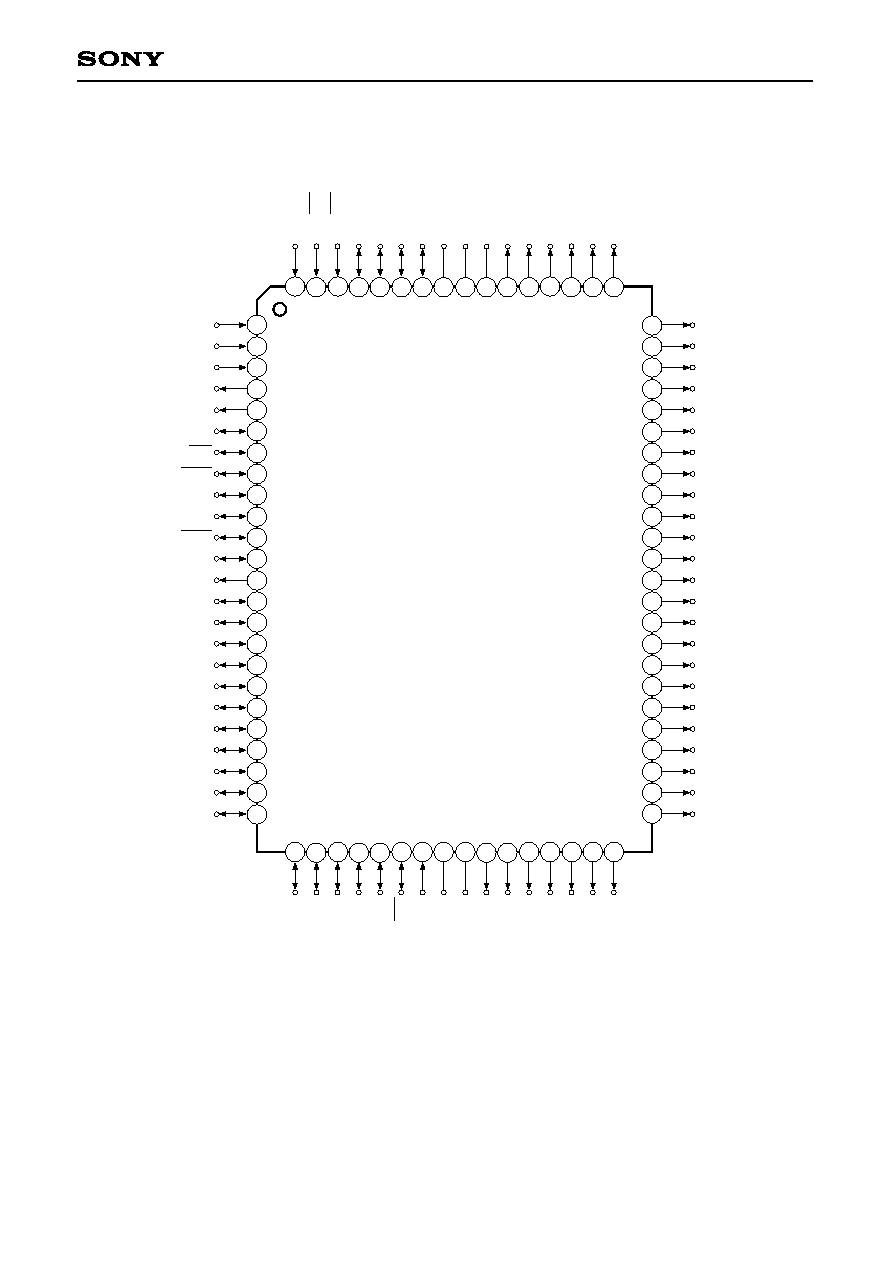
CXP823P24
≠ 4 ≠
Pin Description
(Port A)
8-bit port; single bit
addressable.
(8 pins)
(Port B)
Single bit addressable from
amongst lower 7 bits;
highest bit (PB7)
dedicated to output.
(8 pins)
(Port C)
8-bit port; single bit
addressable. Can provide
12mA sink current.
(8 pins)
(Port E)
8-bit port with lower 6 bits
dedicated to input and
upper 2 bits dedicated to
output.
(8 pins)
Analog input to A/D converter.
(8 pins)
External capture input for 16-bit timer/counter.
Chip select input for serial interface (CH0).
Serial clock (CH0) input/output.
Serial data (CH0) input.
Serial data (CH0) output.
Serial clock (CH1) input/output.
Serial data (CH1) input.
Serial data (CH1) output.
Key return input for FDP segment signal
which performs key scanning.
Input for external
interrupt requests.
(4 pins)
Input for remote control receiving circuit.
Output pin for 16-bit timer/counter
rectangular waveform.
Symbol
I/O
Description
PA0/AN0
to
PA7/AN7
PB0/CINT
PB1/CS0
PB2/SCK0
PB3/SI0
PB4/SO0
PB5/SCK1
PB6/SI1
PB7/SO1
PC0/KR0
to
PC7/KR7
PE0/INT0/EC0
PE1/INT1/EC1
PE2/INT2
PE3/INT3
PE4/RMC
PE5
PE6
PE7/TO
PG0 to PG3
PF0/S8
to
PF7/S15
S16 to S20
T8/S28
to
T15/S21
T0 to T7
PD0/S0
to
PD7/S7
I/O/Analog input
I/O/Input
I/O/Input
I/O/I/O
I/O/Input
I/O/Output
I/O/I/O
I/O/Input
Output/Output
I/O/Input
Input/Input/Input
Input/Input/Input
Input/Input
Input/Input
Input/Input
Input
Output
Output/Output
I/O
Output/Output
Output
Output/Output
Output
Output/Output
(Port G)
4-bit input/output port; single bit addressable.
(4 pins)
(Port F)
8-bit dedicated output port.
(8 pins)
Segment signal output for FDP.
Dual purpose output for FDP timing and segment signals.
Timing signal output for FDP.
(Port D)
8-bit dedicated output port.
(8 pins)
Segment signal output for FDP.
External event input
to timer/counter.
(2 pins)
Segment signal
output for FDP.
≠ 5 ≠
CXP823P24
Provides voltage for FDP.
Connection for system clock oscillation crystal. When using an external
clock, input normal signal to EXTAL and reverse phase signal to the
XTAL pin.
System reset, active "L". The RST pin is an input/output pin which
outputs a "L" level from the on-chip power on reset circuit when the
power is turned on.
Positive power supply for the programmable on-chip PROM; connect to
V
DD
for nomal operation.
Positive power supply pin.
GND
Symbol
I/O
Description
Input
Output
I/O
V
FDP
EXTAL
XTAL
RST
Vpp
V
DD
V
SS
≠ 6 ≠
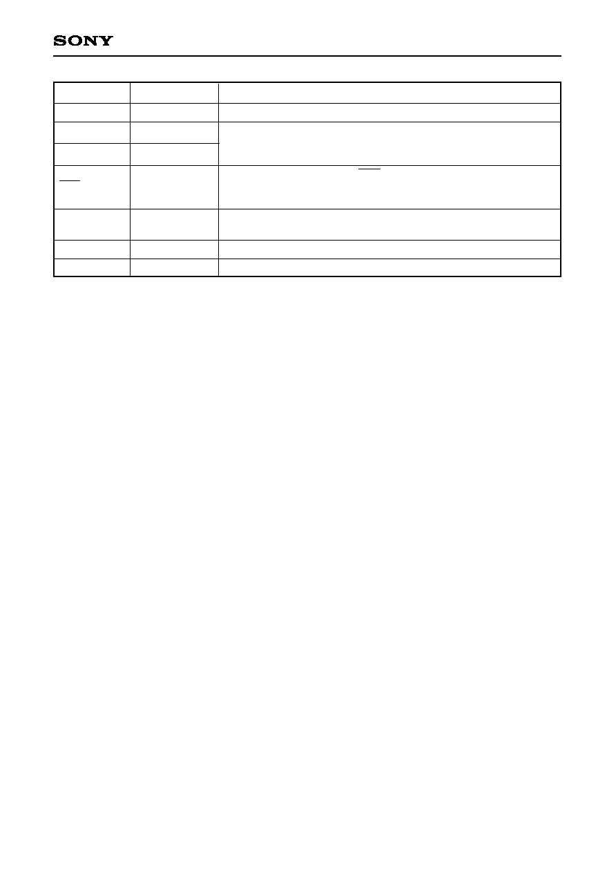
CXP823P24
When reset
Pin
Circuit format
Input/Output Circuit Formats for Pins
IP
RD (Port B)
Data bus
Port B direction
Port B output select
"0" when reset
SCK in
Schmitt input
Port B data
"0" when reset
SCK OUT
Output enable
Hi-Z
Hi-Z
Hi-Z
PB0/CINT
PB1/CS0
PB3/SI0
PB6/SI1
PB2/SCK0
PB5/SCK1
Port B
Port B
2 pins
Port A
IP
Input multiplexer
RD (Port A)
Data bus
Port A direction
Port A data
"0" when reset
Port A input select
"0" when reset
A/D converter
Input
protection
circuit
IP
RD (Port B)
Data bus
Port B direction
Port B data
"0" when reset
CINT
CS0
SI0
SI1
Schmitt input
PA0/AN0
to
PA7/AN7
8 pins
4 pins
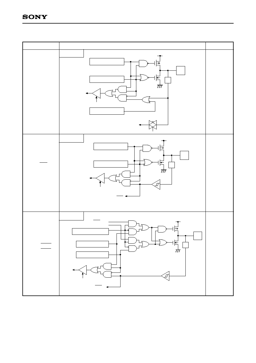
≠ 7 ≠
CXP823P24
When reset
Pin
Circuit format
IP
RD (Port B)
Data bus
Port B direction
Port B output select
"0" when reset
Port B data
"0" when reset
SO
Output enable
Port B
Port C
Port E
1 pin
High level
Hi-Z
Hi-Z
PB4/SO0
PB7/SO1
1 pin
8 pins
Hi-Z
PC0/KR0
to
PC7/KR7
5 pins
PE0/EC0/INT0
PE1/EC1/INT1
PE2/INT2
PE3/INT3
PE4/RMC
Port B
IP
RD (Port C)
Data bus
Port C direction
Port C data
"0" when reset
Key input signal
Capable of driving 12mA large current
RD (Port E)
IP
EC0/INT0
EC1/INT1
INT2
INT3
RMC
Data bus
Schmitt input
RD (Port B)
Data bus
Port B output select
"1" when reset
Port B data
"0" when reset
SO
Output enable
Internal reset signal
Pull-up transistor
approx. 200k
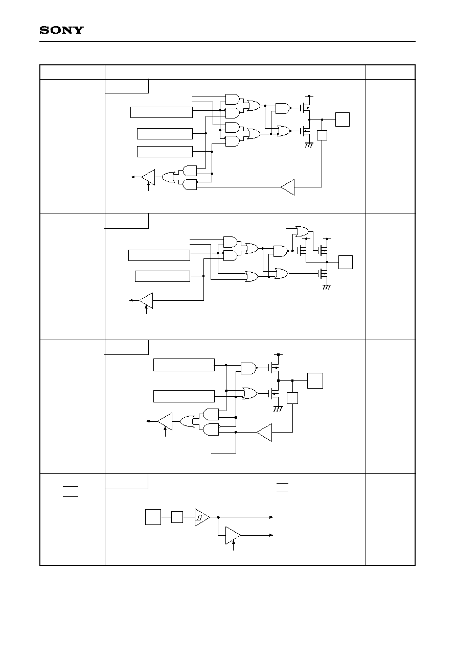
≠ 8 ≠
CXP823P24
When reset
Pin
Circuit format
Port E
Port E
Port E
Hi-Z
1 pin
PE5
IP
Data bus
RD (Port E)
High level
1 pin
PE6
Port E data
"1" when reset
High level
1 pin
PE7/TO
Port G
Hi-Z
4 pins
PG0
to
PG3
RD (Port E)
Data bus
Port E output select
"1" when reset
Port E data
"0" when reset
Output enable (T2OE)
TO
IP
RD (Port G)
Data bus
Port G direction
Port G data
"0" when reset
≠ 9 ≠
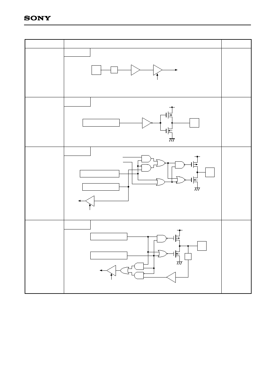
CXP823P24
V
FDP
("0" when reset)
Segment output data
Output selection control signal
High voltage tolerance transistor
Mask option
Pull-down
resistor
OP
21 pins
Oscillation
Low level
When reset
S16 to S20
T15/S21
to
T8/S28
T0 to T7
EXTAL
XTAL
2 pins
1 pin
RST
Hi-Z or
Low level
(when pull-
down resistor
is connected)
Port D
Port F
Pin
Circuit format
IP
IP
EXTAL
XTAL
Diagram shows
circuit construction
for oscillation.
During stop
feedback resistor is
disconnected.
Mask option
IP
Schmitt input
Pull-up resistor
From power on reset circuit
(Mask option)
OP
Hi-Z or
Low level
(when pull-
down resistor
is connected)
16 pins
PD0/S0
to
PD7/S7
PF0/S8
to
PF7/S15
V
FDP
RD (Port D or Port F)
Data bus
"0" when reset
Port D data or
Port F data
("0" when reset)
Segment output data
Output selection control signal
High voltage tolerance transistor
Mask option
Pull-down
resistor
OP
≠ 10 ≠
CXP823P24
1
V
IN
and V
OUT
cannot exceed V
DD
+ 0.3V.
2
Rating for output current of general input/output port.
3
The large current drive transistor is an N-channel transistor of Port C.
Note) If the absolute maximum ratings are exceeded, the LSI could reach permanent breakdown. Also,
observing recommended operating conditions is desirable; otherwise, the LSI's reliability could be
affected.
Supply voltage
Input voltage
Output voltage
Display output voltage
High level output current
High level total output current
Low level output current
Low level total output current
Operating temperature
Storage temperature
Allowable power dissipation
V
DD
Vpp
V
IN
V
OUT
V
OD
I
OH
I
ODH1
I
ODH2
I
OH
I
ODH
I
OL
I
OLC
I
OL
Topr
Tstg
P
D
Incorporated PROM
As P channel transistor is open drain,
V
DD
voltage is determined as standerd.
Other than display output pins
2
: per pin
Display outputs S0 to S20: per pin
Display outputs T0 to T7,
T8/S28 to T15/S21: per pin
Total of other than display output pins
Total of display output pins
Port 1 pin
Large current port pin
3
Entire pin total
Item
Symbol
Rating
Unit
Remarks
Absolute Maximum Ratings
(Vss = 0V)
≠0.3 to +7.0
≠0.3 to +13.0
≠0.3 to +7.0
1
≠0.3 to +7.0
1
V
DD
≠ 40 to
V
DD
+ 0.3
≠5
≠15
≠35
≠40
≠100
15
20
100
≠10 to +75
≠55 to +150
600
V
V
V
V
V
mA
mA
mA
mA
mA
mA
mA
mA
∞C
∞C
mW
≠ 11 ≠
CXP823P24
High level input
voltage
Low level input
voltage
Operating temperature
Supply voltage
5.5
5.5
5.5
V
DD
V
DD
V
DD
+ 0.3
0.3V
DD
0.2V
DD
0.4
+75
V
V
V
V
V
V
V
∞C
V
Item
Symbol
Min.
Max.
Unit
Remarks
4.5
3.5
2.5
0.7V
DD
0.8V
DD
V
DD
≠ 0.4
0
0
≠0.3
≠10
Vpp
V
IH
V
IHS
V
IHEX
V
IL
V
ILS
V
ILEX
Topr
High-speed mode (1/2, 1/4 clock) guaranteed
range during operation
Low-speed mode (1/16 clock) guaranteed range
during operation
Guaranteed data hold operation range during stop
4
1
Hysteresis input
2
EXTAL pin
3
1
Hysteresis input
EXTAL pin
3
V
DD
1
All regular input ports (PA, PB3, PB4, PB6, PC, PE5, PG).
2
For pins RST, CINT, CS0, SCK0, SCK1, EC0/INT0, EC1/INT1, INT2, INT3, RMC.
3
Rating only for external clock input.
4
Vpp and V
DD
should be set to the same voltage.
Recommended Operating Conditions
(Vss = 0V)
Vpp = V
DD
≠ 12 ≠
CXP823P24
V
DD
= 4.5V, I
OH
= ≠0.5mA
V
DD
= 4.5V, I
OH
= ≠1.2mA
V
DD
= 4.5V, I
OL
= 1.8mA
V
DD
= 4.5V, I
OL
= 3.6mA
V
DD
= 4.5V, I
OL
= 12.0mA
V
DD
= 5.5V, V
IH
= 5.5V
V
DD
= 5.5V, V
IL
= 0.4V
V
DD
= 5.5V, V
IL
= 0.4V
High level
output voltage
4.0
3.5
0.5
≠0.5
≠1.5
≠8
≠20
60
V
V
V
V
V
µA
µA
µA
mA
mA
µA
k
µA
mA
mA
µA
pF
PC
EXTAL
RST
Item
Symbol
Pins
Condition
Min.
V
DD
I
DD1
I
DDSL
I
DDST
I
OH
I
LOL
C
IN
V
OH
V
OL
I
IHE
I
ILE
I
ILR
Low level
output voltage
Input current
Typ.
0.4
0.6
1.5
40
≠40
≠400
≠20
270
±
10
40
8
30
20
Max. Unit
Electrical Characteristics
DC Characteristics
(Ta = ≠10 to +75∞C, Vss = 0V)
10MHz crystal
oscillator
(C
1
= C
2
= 15pF)
Sleep mode
Stop mode
Supply current
Input capacitance
V
DD
= 4.5V
V
OH
= V
DD
≠ 2.5V
V
DD
= 5.5V
V
OL
= V
DD
≠ 35V
V
FDP
= V
DD
≠ 35V
V
DD
= 5.5V
High-speed mode
(1/2 clock) operation
1MHz clock
0V other than the measured
Display output
current
I
IZ
Input/output leak
current
Open drain output
leak current
(P-CH Tr off state)
S0 to S20
S21/T15 to S28/T8
T0 to T7
S0 to S20
S21/T15 to S28/T8
T0 to T7
R
L
V
DD
= 5V
V
OD
≠ V
FDP
= 30V
V
DD
= 5.5V
V
I
= 0, 5.5V
Pull-down
resistor
S0 to S20
S21/T15 to S28/T8
T0 to T7
PA to PC, PE, PG
100
25
3
10
PA, PB, PC, PE6,
PE7, PG, RST
(for V
OL
only)
For pins other
than S0 to S28,
T0 to T7, PB7,
PE6, PE7, V
DD
,
V
SS
, V
FDP
All output pins are left open.
≠ 13 ≠
CXP823P24
1
t
sys is determind by the upper two bits of the clock control resister (Address: 00FE
H
; CPU clock selected)
resulting in one of the 3 following values:
t
sys [ns] = 2000/fc (Upper 2 bits = "00"), 4000/fc (Upper 2 bits = "01"), 16000/fc (Upper 2 bits= "11")
EXTAL
t
XH
t
XL
t
CF
t
CR
0.4V
V
DD
≠ 0.4V
1/fc
External clock
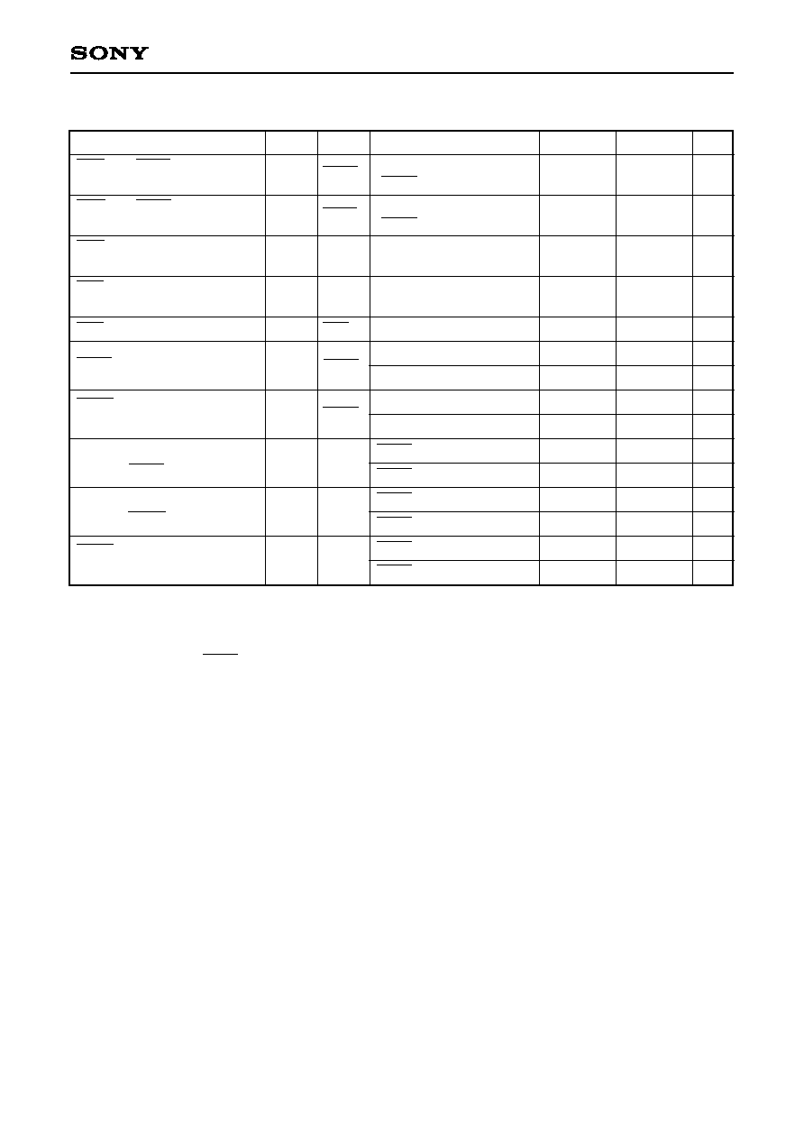
EXTAL
XTAL
74HC04
Crystal oscillation
Ceramic oscillation
EXTAL
XTAL
C
1
C
2
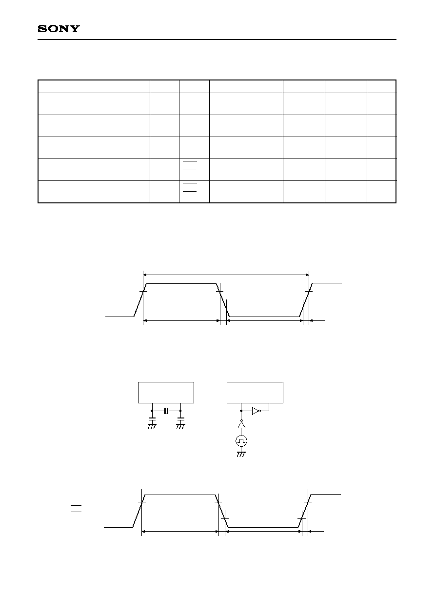
AC Characteristics
(1) Clock timing
System clock frequency
System clock input pulse width
System clock input rising and
falling times
Event count input clock pulse
width
Event count input clock rising
and falling times
f
C
t
XL
,
t
XH
t
CR
,
t
CF
t
EH
,
t
EL
t
ER
,
t
EF
XTAL
EXTAL
EXTAL
EXTAL
EC0,
EC1
EC0,
EC1
MHz
ns
ns
ns
ms
Item
Symbol
Pins
Conditions
Unit
Fig. 1, Fig. 2
Fig. 1, Fig. 2
External clock driver
Fig. 1, Fig. 2
External clock driver
Fig. 3
Fig. 3
Min.
1
45
t
sys
+
50
1
Max.
10
200
20
(Ta = ≠10 to +75∞C, V
DD
= 4.5 to 5.5V, Vss = 0V)
Fig. 1. Clock timing
Fig. 2. Clock applying condition
t
EH
t
EL
t
EF
t
ER
0.2V
DD
0.8V
DD
t
TH
t
TL
t
TF
t
TR
EC0
EC1
Fig. 3. Event count clock timing
≠ 14 ≠
CXP823P24
Chip select transfer mode
(SCK0 = output mode)
Chip select transfer mode
(SCK0 = output mode)
Chip select transfer mode
Chip select transfer mode
Chip select transfer mode
Input mode
Output mode
Input mode
Output mode
SCK0 input mode
SCK0 output mode
SCK0 input mode
SCK0 output mode
SCK0 input mode
SCK0 output mode
Note 1)
t
sys is determind by the upper two bits of the clock control resister (Address: 00FE
H
; CPU clock
selected) resulting in one of the 3 following values:
t
sys [ns] = 2000/fc (Upper 2 bits = "00"), 4000/fc (Upper 2 bits = "01"), 16000/fc (Upper 2 bits = "11")
Note 2)
The load of SCK0 output mode and SO0 output delay time is 50pF + 1TTL.
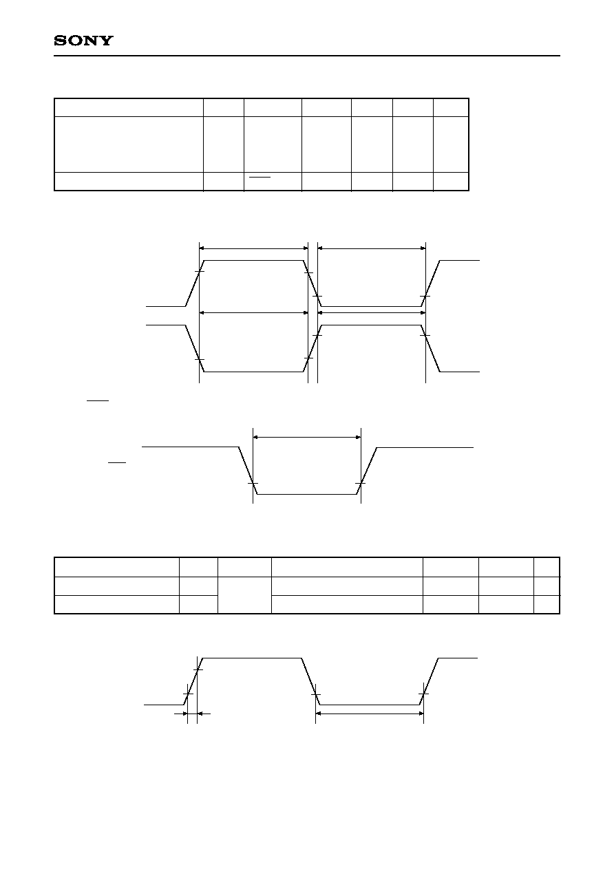
(2) Serial transfer (CH0)
(Ta = ≠10 to +75∞C, V
DD
= 4.5 to 5.5V, Vss = 0V)
Item
CS0
SCK0
delay time
CS0
SCK0
float delay time
CS0
SO0
delay time
CS0
SO0
float delay time
CS0 high level width
SCK0 cycle time
SCK0
high and low level width
SI0 input setup time
(against SCK0
)
SI0 input hold time
(against SCK0
)
SCK0
SO0
delay time
t
DCSK
t
DCSKF
t
DCSO
t
DCSOF
t
WHCS
t
KCY
t
KH
t
KL
t
SIK
t
KSI
t
KSO
SCK0
SCK0
SO0
SO0
CS0
SCK0
SCK0
SI0
SI0
SO0
Symbol
Pin
Min.
t
sys + 200
t
sys + 200
t
sys + 200
t
sys + 200
t
sys + 200
100
t
sys + 200
2
t
sys + 200
16000/fc
t
sys + 100
8000/fc ≠ 50
100
200
t
sys + 200
100
ns
ns
ns
ns
ns
ns
ns
ns
ns
ns
ns
ns
ns
ns
ns
Max.
Unit
Condition
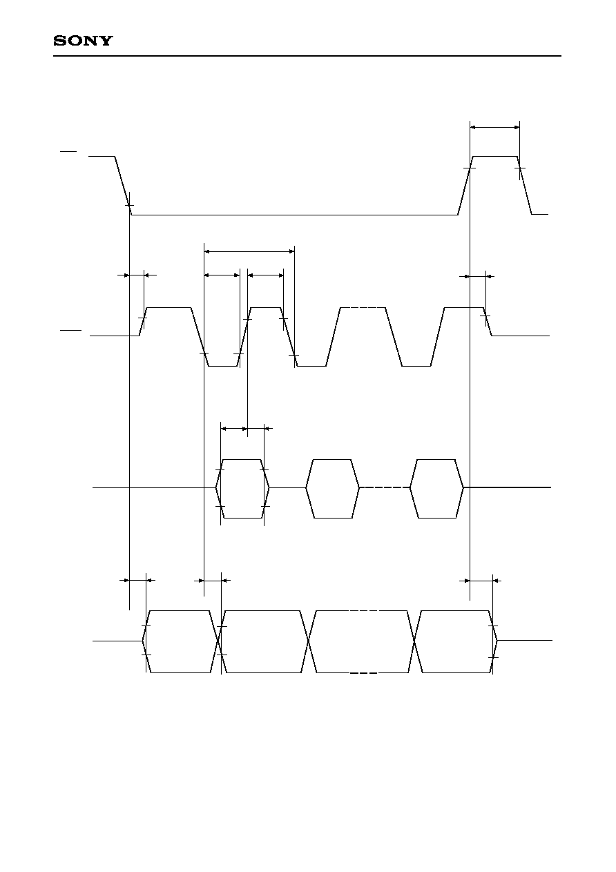
CXP823P24
Fig. 4. Serial transfer CH0 timing
CS0
SCK0
0.2V
DD
0.8V
DD
t
WHCS
t
DCSK
t
DCSKF
0.8V
DD
0.2V
DD
0.8V
DD
t
KCY
t
KL
t
KH
0.8V
DD
0.2V
DD
SI0
t
SIK
t
KSI
Input
data
t
DCSO
t
KSO
t
DCSOF
Output data
0.8V
DD
0.2V
DD
SO0
≠ 15 ≠
≠ 16 ≠
CXP823P24
Serial transfer (CH1)
(Ta = ≠10 to +75∞C, V
DD
= 4.5 to 5.5V, Vss = 0V)
Item
Symbol
Pin
Min.
Max.
Condition
SCK1 cycle time
SCK1 high and low
level width
SI1 input setup time
(against SCK1
)
SI1 input hold time
(against SCK1
)
SCK1
SO1 delay time
t
KCY
t
KH
t
KL
t
SIK
t
KSI
t
KSO
SCK1
SCK1
SI1
SI1
SO1
Input mode
Output mode
Input mode
Output mode
SCK1 input mode
SCK1 output mode
SCK1 input mode
SCK1 output mode
SCK1 input mode
SCK1 output mode
1000
16000/fc
400
8000/fc ≠ 50
100
200
200
100
200
100
Unit
ns
ns
ns
ns
ns
ns
ns
ns
ns
ns
Note) The load of SCK1 output mode and SO1 output delay time is 50pF + 1TTL.
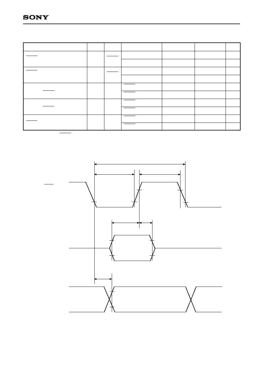
Fig. 5. Serial transfer CH1 timing
SCK1
SI1
SO1
t
KCY
t
KL
t
KH
0.2V
DD
0.8V
DD
t
SIK
t
KSI
t
KSO
Input data
Output data
0.2V
DD
0.8V
DD
0.2V
DD
0.8V
DD
≠ 17 ≠
CXP823P24
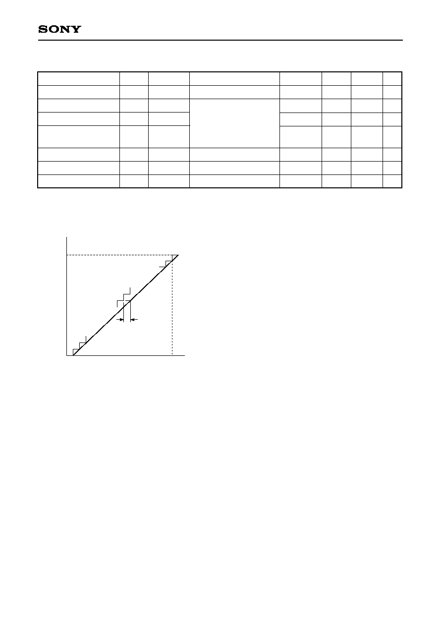
(3) A/D converter characteristics
(Ta = ≠10 to +75∞C, V
DD
= 4.5 to 5.5V, Vss = 0V)
V
ZT
1
V
FT
2
t
CONV
t
SAMP
V
IAN
A/D converter operation
only
Ta = 25∞C
V
DD
= 5.0V
V
SS
= 0V
≠10
4930
160/f
ADC
3
12/f
ADC
3
0
Item
Symbol
Pin
Condition
Min.
Typ.
Max.
Unit
Bits
Resolution
Linearity error
Zero transition voltage
Full-scale transition
voltage
Conversion time
Sampling time
Analog input voltage
8
±3
150
5120
V
DD
70
5050
LSB
mV
mV
µs
µs
V
Analog input
Linearity error
00
H
01
H
FE
H
FF
H
Digital conversion value
V
ZT
V
FT
Fig. 6. Definition of A/D converter terms
AN0 to AN7
1
V
ZT
: Digital Value converted between 00
H
to 01
H.
2
V
FT
: Digital Value converted between FE
H
and FF
H
.
3
f
ADC
: ADC operation clock selection (MSC: Bit 0 of
address 01FF
H
) and assumes following values:
f
ADC
= fc/2 when PS2 is selected.
f
ADC
= fc when PS1 is selected.
≠ 18 ≠
CXP823P24
External interrupt High and
Low level widths
Reset input Low level width
INT0
INT1
INT2
INT3
RST
1
8/fc
µs
µs
Item
Symbol
Pin
Condition
Min.
Max.
Unit
t
IH
t
IL
t
RSL
(4) Interrupts, reset inputs
(Ta = ≠10 to +75∞C, V
DD
= 4.5 to 5.5V, Vss = 0V)
0.8V
DD
0.2V
DD
t
IH
t
IL
INT0
INT1
INT2
INT3
t
IL
t
IH
0.8V
DD
0.2V
DD
Fig. 7. Interrupt input timing
t
RSL
0.2V
DD
RST
Fig. 8. RST input timing
0.2V
0.2V
4.5V
V
DD
t
OFF
t
R
The power supply should rise smoothly.
Fig. 9. Power-on reset
Power supply rising time
Power supply cut-off time
t
R
t
OFF
V
DD
Item
Symbol
Pin
Condition
Min.
Max.
Unit
ms
ms
(5) Power-on reset
Power-on reset
(Ta = ≠10 to +75∞C, V
DD
= 4.5 to 5.0V, V
SS
= 0V)
50
Power-on reset
Repetitive power-on reset
0.05
1
≠ 19 ≠
CXP823P24
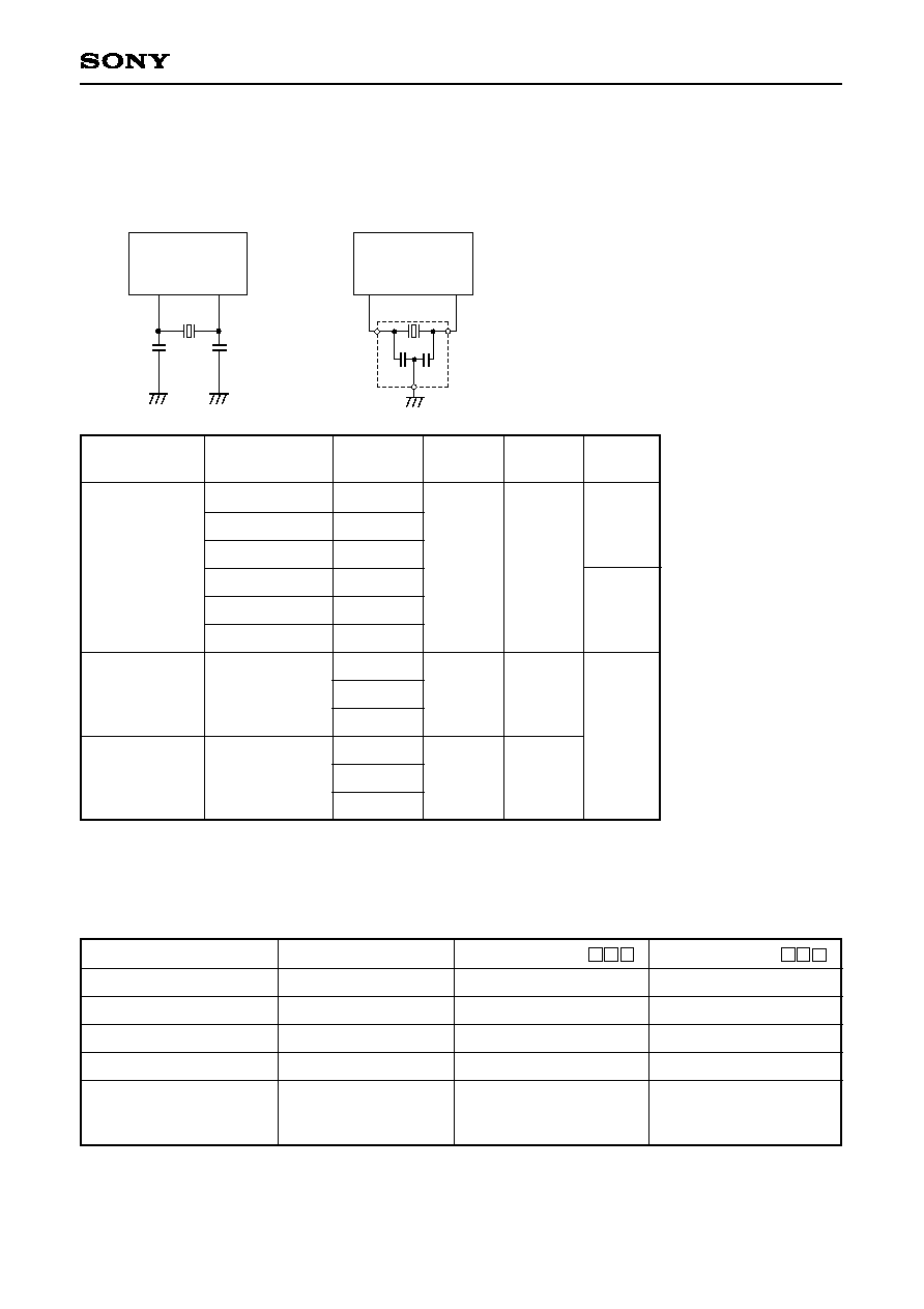
Supplement
Fig. 10. Recommended Oscillation Circuit
EXTAL
XTAL
C
1
C
2
(i)
EXTAL
XTAL
C
2
(ii)
C
1
Manufacturer
MURATA MFG
CO., LTD
RIVER
ELETEC
CORPORATION
KINSEKI LTD.
CSA4.19MG
CSA8.00MTZ
CSA10.0MTZ
CST4.19MGW
CST8.00MTW
CST10.0MTW
HC-49/U03
HC-49/U (-S)
Model
fc (MHz)
4.19
8.00
10.00
4.19
8.00
10.00
4.19
8.00
10.00
4.19
8.00
10.00
30
15
27
30
15
27
C
1
(pF) C
2
(pF)
Circuit
Example
(i)
(ii)
(i)
Indicates types with on-chip grounding capacitors (C
1
and C
2
).
Optional item
Mask
CXP823P24Q-1-
Package
ROM capacity
Reset pin pull-up resistor
Power-on reset circuit
High voltage tolerance pin
pull-down resistor
80 pin plastic QFP
20K bytes/24K bytes
Existent/Non-existent
Existent/Non-existent
Existent/Non-existent
80 pin plastic QFP
PROM 24K bytes
Existent
Existent
Non-existent
(S0/PD0 to S15/PF7)
Existent (T0 to S16)
80 pin plastic QFP
PROM 24K bytes
Existent
Existent
Existent
(High voltage tolerance pin)
Product List
CXP823P24Q-2-
≠ 20 ≠
CXP823P24
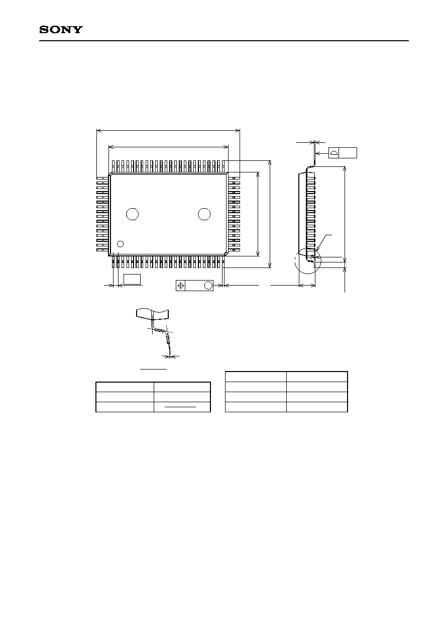
Package Outline
Unit: mm
PACKAGE STRUCTURE
SONY CODE
EIAJ CODE
JEDEC CODE
QFP-80P-L01
QFP080-P-1420
PACKAGE MATERIAL
LEAD TREATMENT
LEAD MATERIAL
PACKAGE MASS
EPOXY RESIN
SOLDER PLATING
42/COPPER ALLOY
1.6g
23.9 ± 0.4
20.0 ≠ 0.1
+ 0.4
1
80
65
64
41
40
25
24
0.8
0.35 ≠ 0.1
+ 0.15
14.0 ≠ 0.1
+ 0.4
17.9 ±
0.4
16.3
0.1 ≠ 0.05
+ 0.2
2.75 ≠ 0.15
+ 0.35
0.8 ±
0.2
0.15 ≠ 0.05
+ 0.1
80PIN QFP (PLASTIC)
M
0.2
0.15
0∞ to 10∞
DETAIL A
A