Description
The CXP82600 is a CMOS 8-bit single chip
microcomputer of piggyback/evaluator combined
type, which is developed for evaluating the function
of the CXP82612/82616.
Features
∑ A wide instruction set (213 instructions) which
cover various types of data.
-- 16-bit operation/multiplication and division/boolean bit operation instructions
∑ Minimum instruction cycle
400ns at 10MHz operation
122µs at 32kHz operation
∑ Applicable EPROM
LCC type 27C128, LCC type 27C256
(Maximum 16K bytes are available.)
∑ Incorporated RAM capacity
448 bytes ( fluorescent display data area included)
∑ Peripheral functions
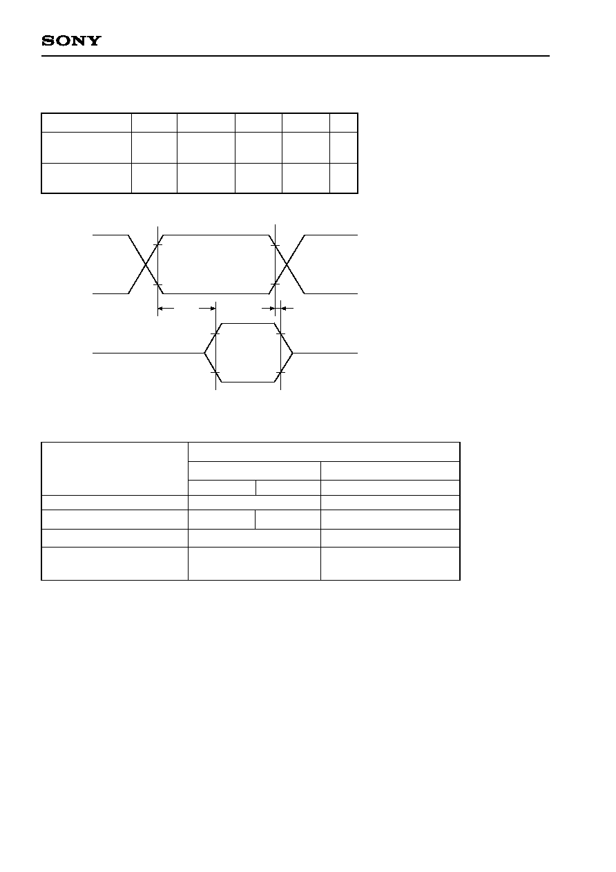
-- A/D converter
8-bit, 8-channel, successive approximation method
(Conversion time of 32µs/10MHz)
-- Serial interface
Incorporated 8-bit and 8-stage FIFO
(Auto transfer for 1 to 8 bytes), 1 circuit 2channels
-- Timer
8-bit timer, 8-bit timer/counter,
19-bit time base timer, 32kHz timer/counter
-- Fluorescent display panel controller/driver
Maximum 336 segments display possible
1 to 16-digit dynamic display
Dimmer function
High voltage drive output (40V)
On-chip pull-down resistor (Mask option)
Hardware key scan function
(Maximum 8
◊
16 key matrix compatible.)
-- Remote control receiving circuit
8-bit pulse measurement counter with on-chip
6-stage FIFO
∑ Interruption
13 factors, 13 vectors, multi-interruption possible
∑ Standby mode
SLEEP/STOP
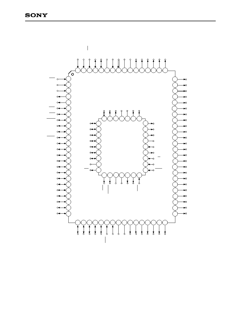
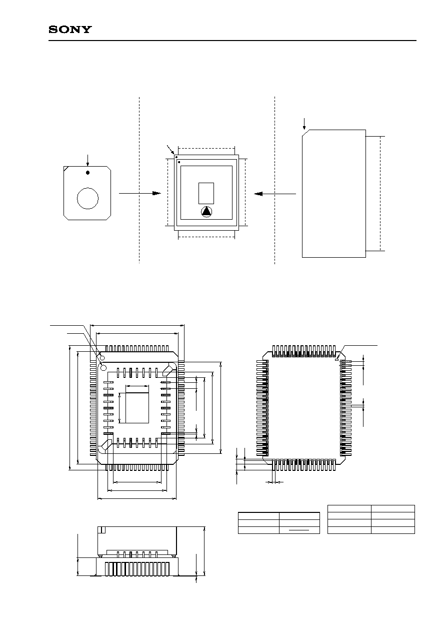
∑ Package
80-pin ceramic PQFP
Note) Mask option depends on the type of the CXP82600. Refer to the Products List for details.
Structure
Silicon gate CMOS IC
≠ 1 ≠
CXP82600
E94X10-PP
CMOS 8-bit Single Chip Microcomputer
Sony reserves the right to change products and specifications without prior notice. This information does not convey any license by
any implication or otherwise under any patents or other right. Application circuits shown, if any, are typical examples illustrating the
operation of the devices. Sony cannot assume responsibility for any problems arising out of the use of these circuits.
80 pin PQFP (Ceramic)
Piggyback/
evaluator type