 | –≠–ª–µ–∫—Ç—Ä–æ–Ω–Ω—ã–π –∫–æ–º–ø–æ–Ω–µ–Ω—Ç: CXP82960 | –°–∫–∞—á–∞—Ç—å:  PDF PDF  ZIP ZIP |
≠ 1 ≠
CXP82940/82948/82952/82960
E95130-PK
CMOS 8-bit Single Chip Microcomputer
Description
The CXP82940/82948/82952/82960 is a CMOS 8-bit
single chip microcomputer integrating on a single
chip an A/D converter, serial interface, timer/counter,
time base timer, fluorescent display panel
controller/driver, I
2
C bus interface, remote control
transmission circuit, remote control reception circuit,
and 32kHz timer/counter besides the basic
configurations of 8-bit CPU, ROM, RAM, and I/O
port.
Features1
∑ Wide-range instruction system (213 instructions)
to cover various types of data
-- 16-bit arithmetic/multiplication and division/boolean bit operation instructions
∑ Minimum instruction cycle
250ns at 16MHz operation
(122µs at 32kHz operation)
∑ Incorporated ROM capacity
40K bytes (CXP82940)
48K bytes (CXP82948)
52K bytes (CXP82952)
60K bytes (CXP82960)
∑ Incorporated RAM capacity
2048 bytes (including fluorescent display area)
∑ Periphera; functions
-- A/D converter
8-bit, 8-channel, successive approximation method
(Conversion time of 20µs/16MHz)
-- Serial interface
Buffer RAM incorporated (Auto transfer for 1 to 32 bytes), 1 channel
8-bit, 8-stage FIFO incorporated
(Auto transfer for 1 to 8 bytes), 1 channel
-- Timers
8-bit timer, 8-bit timer/counter, 19-bit time base timer
32kHz timer/counter
-- Fluorescent display panel controller/driver
Maximum of 196 segments display possible
1 to 16-digit dynamic display
Dimmer function
High voltage drive output (40V)
Incorporated pull-down resistor (Mask option)
Hardware key scan function
Maximum of 12
◊
8 key matrix supportable
-- I
2
C bus interface
-- Remote control transmission circuit
Auto transmission for 1 to 32 bytes,
restart function, carrier output function
-- Remote control reception circuit
8-bit pulse measurement counter, 6-stage FIFO
∑ Interruption
16 factors, 15 vectors, multi-interruption possible
∑ Standby mode
SLEEP/STOP
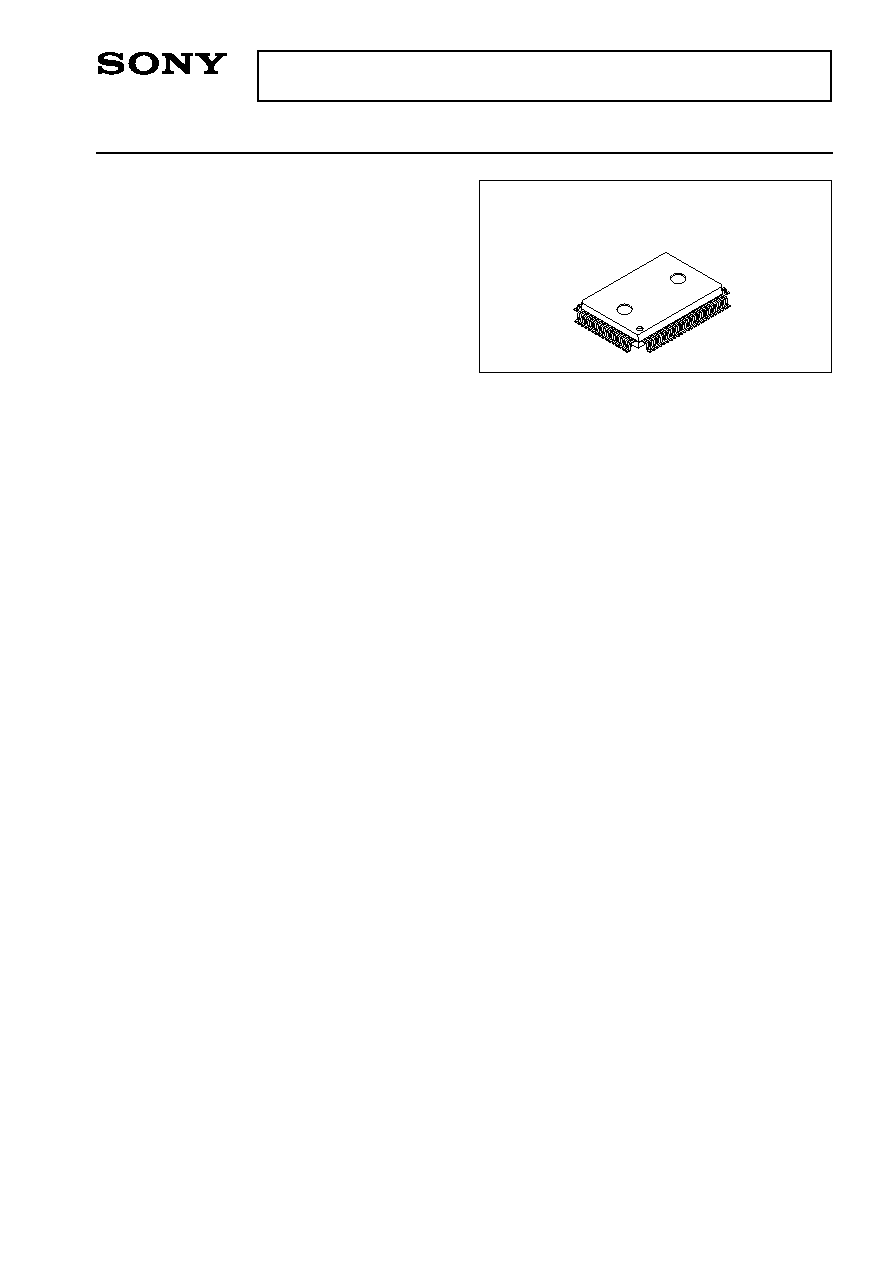
∑ Package
80-pin plastic QFP
∑ Piggyback/evaluation chip
CXP82900 80-pin ceramic QFP
Perchase of Sony's I
2
C components conveys a licence under the Philips I
2
C Patent Rights to use these components
in an I
2
C system, provided that the system conforms to the I
2
C Standard Specifications as defined by Philips.
Sony reserves the right to change products and specifications without prior notice. This information does not convey any license by
any implication or otherwise under any patents or other right. Application circuits shown, if any, are typical examples illustrating the
operation of the devices. Sony cannot assume responsibility for any problems arising out of the use of these circuits.
80 pin QFP (Plastic)
Structure
Silicon gate CMOS IC

≠ 2 ≠
CXP82940/82948/82952/82960
RAM
2048 BYTES
SPC 700
CPU CORE
INTERRUPT CONTROLLER
A/D CONVERTER
SERIAL
INTERFACE
UNIT (CH0)
SERIAL
INTERFACE
UNIT (CH1)
8 BIT TIMER/COUNTER 0
8 BIT TIMER 1
I
2
C BUS
INTERFACE UNIT
INT3/NMI
INT1
INT0
INT2
AN0 to AN7
8
PA0 to PA7
BUFFER
RAM
REMOCON IN
FDP
CONTROLLER/
DRIVER
32KHz
TIMER/COUNTER
PRESCALER/
TIME BASE TIMER
RST
V
DD
V
SS
PORT A
PORT B
PORT C
PORT D
PORT E
PORT F
PORT G
8
8
6
2
4
4
8
8
PB0 to PB7
PC0 to PC7
PD0 to PD7
PE0 to PE5
PF0 to PF3
PG0 to PG3
PE6 to PE7
TEX
EXTAL
XTAL
TX
AV
REF
AV
SS
T0 to T7
T8/S19 to T15/S12
S0 to S11
V
FDP
KR0 to KR7
RMCO
RMC
CS0
SI0
SO0
SCK0
SI1
SO1
SCK1
EC
SCL0
SCL1
SDA0
2
8
8
ROM
40K/48K/52K/60K
BYTES
12
8
RAM
RAM
KEY SCAN
2
CLOCK
GENERATOR
SYSTEM CONTROL
BUFFER
RAM
REMOCON OUT
SDA1
AV
DD
FIFO
FIFO
ADJ
TO
2
Block Diagram
≠ 3 ≠
CXP82940/82948/82952/82960
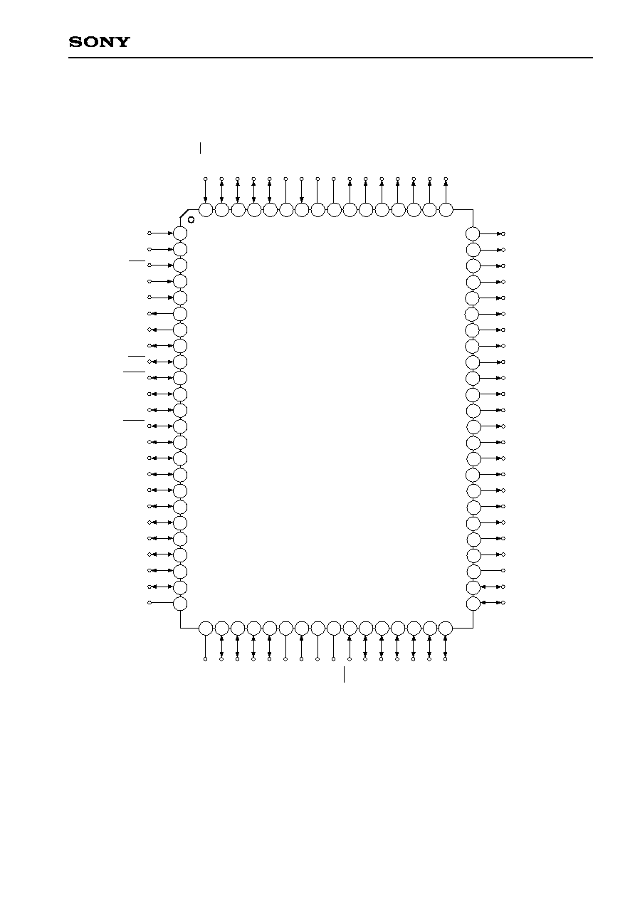
Pin Assignment (Top View)
PE0/EC/INT0
2
3
4
5
6
7
8
9
10
11
12
13
14
15
16
17
18
19
20
21
22
23
24
25 26 27 28 29 30
40
39
38
37
36
35
34
31 32 33
41
42
43
44
45
46
47
48
49
50
51
52
53
54
55
56
57
58
59
60
70 69 68 67
63
64
65
66
61
62
71
72
73
74
75
76
77
78
79
80
1
T0
T1
T2
T3
T4
T5
T6
PB5/SCK1
PB3/SI0
PB4/SO0
PB6/SI1
PB7/SO1
PA7/AN7
PA0/AN0
PA1/AN1
PA2/AN2
PA3/AN3
PA4/AN4
PA5/AN5
PA6/AN6
T7
T10/S17
T11/S16
T12/S15
T13/S14
T14/S13
T15/S12
S11
S10
S9
S8
PD7/S7
PD6/S6
T8/S19
T9/S18
PC6/KR6
PC7/KR7
PD5/S5
PD4/S4
PD3/S3
PD2/S2
PD1/S1
PD0/S0
V
FDP
NC
TEX
TX
V
DD
PG3
PG2
PG1
PG0
PE1/INT1
PE2/INT2
PE3/INT3/NMI
PE4/RMC
PE5
PE6/RMCO
PE7/TO/ADJ
PB0
PB1/CS0
PB2/SCK0
AV
DD
PC0/KR0
PC1/KR1
PC2/KR2
PC3/KR3
PC4/KR4
PC5/KR5
AV
REF
V
SS
AV
SS
PF0/SCL0
PF1/SCL1
PF2/SDA0
PF3/SDA1
EXTAL
XTAL
RST
Note) NC (Pin 75) must be connected to V
DD
.
≠ 4 ≠
CXP82940/82948/82952/82960
Pin Description
Pin code
I/O
Functions
I/O/
Analog input
PA0/AN0
to
PA7/AN7
Analog inputs to A/D converter. (8 pins)
I/O/Input
PC0/KR0
to
PC7/KR7
PE0/INT0/EC
PE1/INT1
PE2/INT2
PE3/INT3/
NMI
PE4/RMC
PE5
PE6/RMCO
PE7/TO/ADJ
PF0/SCL0
PF1/SCL1
PF2/SDA0
PF3/SDA1
Input/Input/Input
Input/Input
Input/Input
Input/Input/Input
Input/Input
Input
Output/Output
Output/Output/
Output
Output/I/O
Output/I/O
Serves as key return inputs when operating
key scan with fluorescent display panel (FDP)
segment signal (8 pins).
(Port E)
8-bit port. Lower 6 bits
are for inputs; upper
2 bits are for outputs.
(8 pins)
(Port F)
4-bit output port,
operating as N-ch open
drain output for large
current (12mA).
(4 pins)
External event inputs for
timer/counter.
Inputs for
external
interruption
request.
(4 pins)
Non-maskable interruption
request input.
Remote control reception circuit input.
Carrier output of remote control transmission
circuit.
Output for the timer/counter rectangular waves,
and 32kHz oscillation dividing frequency.
Transfer clock I/Os for I
2
C bus interface.
Transfer data I/Os for I
2
C bus interface.
I/O
I/O/Input
I/O/I/O
I/O/Input
I/O/Output
I/O/I/O
I/O/Input
I/O/Output
PB0
PB1/CS0
PB2/SCK0
PB3/SI0
PB4/SO0
PB5/SCK1
PB6/SI1
PB7/SO1
(Port B)
8-bit I/O port. I/O can
be set in a unit of
single bits.
Incorporation of pull-up
resistor can be set
through the software in
a unit of 4 bits.
(8 pins)
Chip select input for serial interface (CH0).
Serial clock I/O (CH0).
Serial data input (CH0).
Serial data output (CH0).
Serial clock I/O (CH1).
Serial data input (CH1).
Serial data output (CH1).
(Port A)
8-bit I/O port. I/O can
be set in a unit of
single bits.
Incorporation of pull-up
resistor can be set
through the software in
a unit of 4 bits.
(8 pins)
(Port C)
8-bit I/O port. I/O can
be set in a unit of single
bits. Capable of driving
12mA sync current.
Incorporation of pull-up
resistor can be set
through the software in
a unit of 4 bits.
(8 pins)

≠ 5 ≠
CXP82940/82948/82952/82960
Pin code
I/O
Functions
Output/Output
PD0/S0
to
PD7/S7
(Port D)
8-bit output ports.
(8 pins)
FDP segment signal outputs.
(8 pins)
Output
S8 to S11
FDP segment signal outputs. (4 pins)
Output/Output
T8/S12
to
T15/S19
Outputs for FDP timing signals/segment signals.
(8 pins)
I/O
PG0 to PG3
(Port G)
8-bit I/O port. I/O can be set in a unit of single bits.
Incorporation of pull-up resistor can be set through the software in a unit
of 4 bits.
(4 pins)
V
FDP
EXTAL
XTAL
TEX
TX
RST
NC
AV
REF
AV
SS
V
DD
V
SS
Input
Output
Input
Output
Input
Input
FDP voltage supply when incorporated resistor is set by mask option.
T0 to T7
FDP timing signal outputs.
Crystal connectors for system clock oscillation. When the clock is
supplied externally, input to EXTAL; opposite phase clock should be
input to XTAL.
Crystal connectors for 32kHz timer/counter clock oscillation. Set 32kHz
crystal oscillator between TEX and TX. For usage as event input, attach
clock source to TEX, and open TX.
Low-level active, system reset.
NC. Under normal operation, connect to V
DD
.
AV
DD
Positive power supply for A/D converter.
Reference voltage input for A/D converter.
A/D converter GND.
Positive power supply.
GND.
Output

≠ 6 ≠
CXP82940/82948/82952/82960
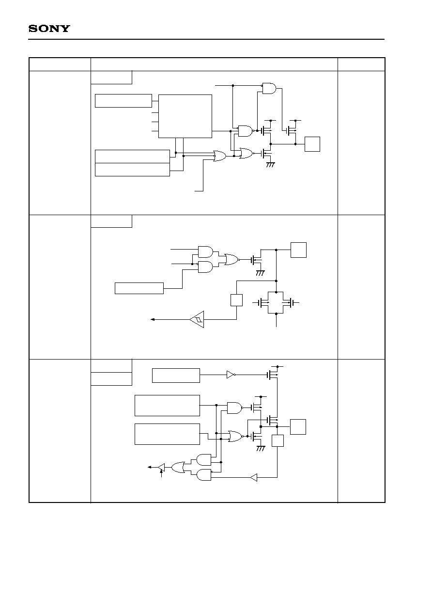
Port B
Data bus
RD (Port B)
Port B direction
IP
Port B data
Pull-up resistor
"0" when reset
"0" when reset
Pull-up transistor approx. 100k
Schmitt input
CS0
SI0
SI1
Not Schmitt input for SI0 and SI1.
8 pins
Hi-Z
Hi-Z
When reset
PA0/AN0
to
PA7/AN7
PB1/CS0
PB3/SI0
PB6/SI1
Port B
Data bus
RD (Port B)
IP
Port B output
selection
"0" when reset
Pull-up transistor approx. 100k
Schmitt input
SCK in
Port B data
Port B direction
"0" when reset
Pull-up resistor
"0" when reset
SCK OUT
Output enable
3 pins
2 pins
Hi-Z
PB2/SCK0
PB5/SCK1
Data bus
RD (Port A)
Port A direction
IP
Port A data
Pull-up resistor
Port A input
selection
Input
protection
circuit
"0" when reset
"0" when reset
"0" when reset
Input multiplexer
A/D converter
Pull-up transistor approx. 100k
Port A
Pin
Circuit format
I/O Circuit Format for Pins
≠ 7 ≠
CXP82940/82948/82952/82960
2 pins
Hi-Z
Hi-Z
PB4/SO0
PB7/SO1
PC0/KR0
to
PC7/KR7
8 pins
5 pins
1 pin
Hi-Z
High level
Hi-Z
PE0/EC/INT0
PE1/INT1
PE2/INT2
PE3/INT3/NMI
PE4/RMC
IP
Schmitt input
RD (Port E)
Data bus
EC/INT0
INT1
INT2
INT3/NMI
RMC
Data bus
RD (Port C)
Port C direction
IP
Port C data
Pull-up resistor
"0" when reset
"0" when reset
1
Large current 12mA
2
Pull-up transistor approx. 100k
2
1
Key input signal
Data bus
RD (Port B)
IP
Port B output
selection
"0" when reset
Pull-up transistor approx. 100k
Port B data
Port B direction
"0" when reset
Pull-up resistor
SO
Output enable
"0" when reset
Port E
PE5
1 pin
PE6/RMCO
IP
RD (Port E)
Data bus
Port E
Port E output selection
RD (Port E)
Data bus
"0" when reset
Reset E data
"1" when reset
Remote control
transmission circuit
Output enable
Port E
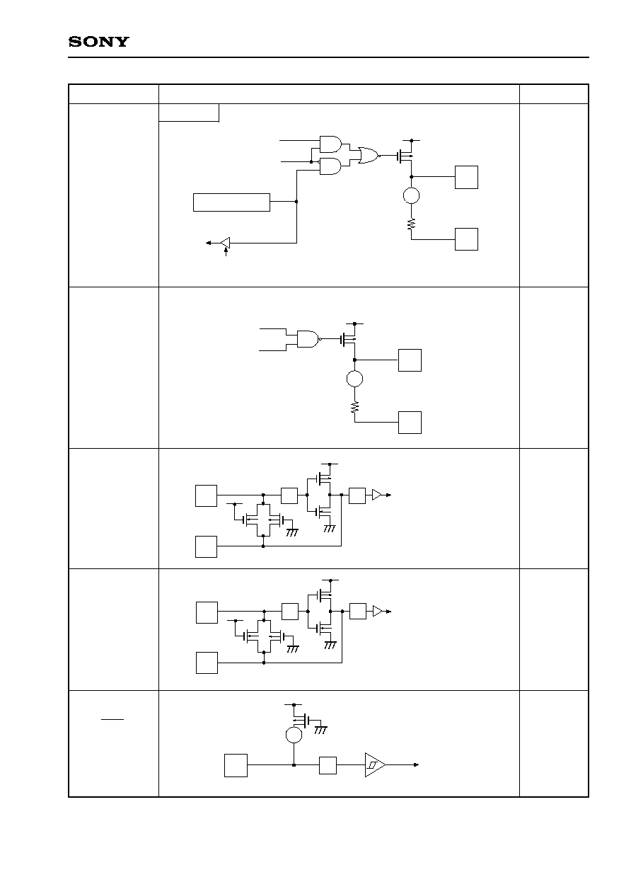
Port C
Port B
When reset
Pin
Circuit format
≠ 8 ≠
CXP82940/82948/82952/82960
1 pin
PE7/TO/ADJ
Port E data
1
ADJ signal is a frequency dividing output for
32kHz oscillation frequency adjustment.
ADJ2 can be used for buzzer output.
2
Pull-up transistor approx. 150k
.
Port E output selection (lower)
"00" when reset
Port E output selection (upper)
TO
ADJ16K
1
ADJ2K
1
TO output enable
01
10
11
00
MPX
Internal reset signal
2
"1" when reset
Port E
4 pins
Hi-Z
PF0/SCL0
PF1/SCL1
PF2/SDA0
PF3/SDA1
SCL, SDA
(I
2
C circuit)
Port F data
SCL, SDA
I
2
C output enable
("0" when reset)
Large current
12mA
To internal I
2
C pin
(to SCL1 for SCL0)
BUS SW
"1" when reset
IP
Schmitt input
Port F
5 pins
Hi-Z
PB0
PG0 to PG3
Data bus
RD (Port B or Port G)
IP
Port B data or
Port G data
"0" when reset
Pull-up transistor approx. 100k
Pull-up resistor
"0" when reset
Port B direction or
Port G direction
Port B
Port G
High level
(with approx.
150k
resistor when
reset)
When reset
Pin
Circuit format
≠ 9 ≠
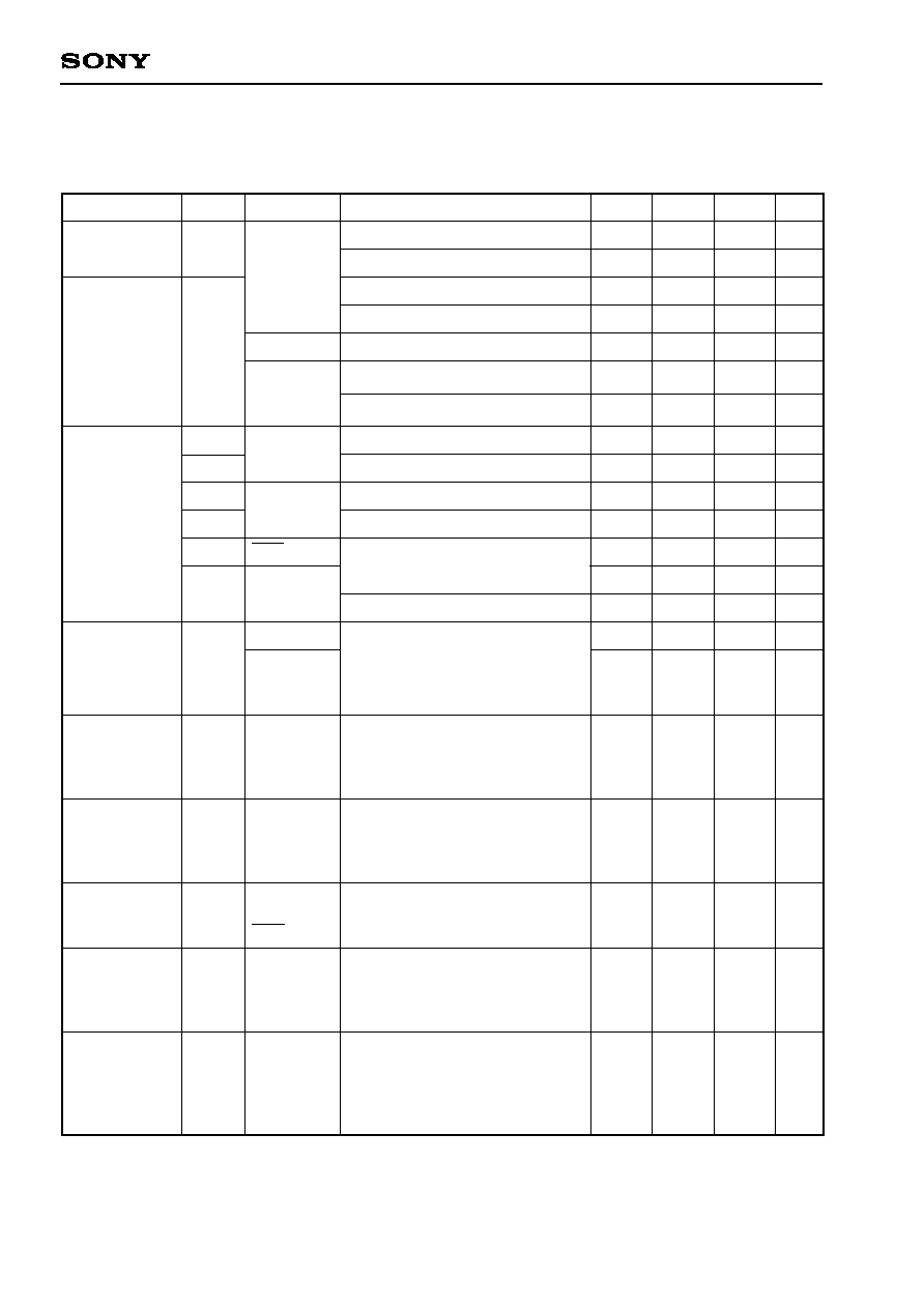
CXP82940/82948/82952/82960
20 pins
Hi-Z or
Low level
(when PD
resistor is
connected)
S8 to S11
T15/S12
to
T8/S19
T0 to T7
Segment output data
Timing output data
Output selection
control signal
("0" when reset)
OP
Mask option
Pull-down
resistor
V
FDP
High voltage drive transistor
2 pins
Oscillation
EXTAL
XTAL
IP
EXTAL
XTAL
∑ Diagram shows circuit
composition during oscillation.
∑ Feedback resistor is removed
during stop, and XTAL
becomes High.
IP
2 pins
Oscillation
TEX
TX
IP
TEX
TX
∑Diagram shows circuit
composition during oscillation.
IP
∑When the operation of the oscillation
circuit is stopped by the software,
the feedback resistor is removed,
and TEX becomes Low level and TX
becomes High level.
1 pin
Low level
RST
Schmitt input
Pull-up resistor
Mask option
OP
IP
8 pins
Hi-Z or
Low level
(when PD
resistor is
connected)
PD0/S0
to
PD7/S7
Data bus
RD (Port D)
Port D data
Segment output data
Output selection
control signal
("0" when reset)
OP
Mask option
Pull-down
transistor
V
FDP
High voltage drive transistor
Port D
When reset
Pin
Circuit format

≠ 10 ≠
CXP82940/82948/82952/82960
1
V
IN
and V
OUT
must not exceed V
DD
+ 0.3V.
2
Specifies output current of general-purpose I/O ports.
3
The large current drive transistor is the N-CH transistor of Port C (PC) and Port F (PF).
Note) Usage exceeding absolute maximum ratings may permanently impair the LSI. Normal operation should be
conducted under the recommended operating conditions. Exceeding these conditions may adversely affect
the reliability of the LSI.
Supply voltage
Input voltage
Output voltage
Display output voltage
High level output current
High level total output
current
Low level output current
Low level total output current
Operating temperature
Storage temperature
Allowable power dissipation
V
DD
V
IN
V
OUT
V
OD
I
OH
I
ODH1
I
ODH2
I
OH
I
ODH
I
OL
I
OLC
I
OL
Topr
Tstg
P
D
≠0.3 to +7.0
≠0.3 to +7.0
1
≠0.3 to +7.0
1
V
DD
≠ 40 to V
DD
+ 0.3
≠5
≠15
≠35
≠40
≠100
15
20
100
≠20 to +75
≠55 to +150
600
V
V
V
V
mA
mA
mA
mA
mA
mA
mA
mA
∞C
∞C
mW
As P channel transistor is open drain,
V
DD
is reference.
All pins excluding outputs
2
(value per pin)
Display outputs S0 to S11 (value per pin)
Display outputs T0 to T7, and T8/S19 to
T15/S12 (value per pin)
Total for all pins excluding display outputs
Total for all display outputs
Port (value per pin)
Large current Port (value per pin)
3
Total for all output pins
Item
Symbol
Rating
Unit
Remarks
Absolute Maximum Ratings
(Vss = 0V reference)

≠ 11 ≠
CXP82940/82948/82952/82960
High level input
voltage
Low level input
voltage
Operating temperature
Supply voltage
5.5
5.5
5.5
5.5
V
DD
V
DD
V
DD
+ 0.3
0.3V
DD
0.2V
DD
0.4
+75
V
V
V
V
V
V
V
V
V
V
∞C
Item
Symbol
Min.
Max.
Unit
Remarks
4.5
3.5
2.7
2.5
0.7V
DD
0.8V
DD
V
DD
≠ 0.4
0
0
≠0.3
≠20
V
IH
V
IHS
V
IHEX
V
IL
V
ILS
V
ILEX
Topr
Guaranteed operation range for high-speed
mode (1/2, 1/4 frequency dividing clock)
Guaranteed operation range for low-speed
mode (1/16 frequency dividing clock) or
SLEEP mode
Guaranteed operation range with TEX
clock
Guaranteed data hold range during STOP
1
Hysteresis input
2
EXTAL
3
1
Hysteresis input
2
EXTAL
3
V
DD
1
Value for each pin of normal input port (PA, PB0, PB3, PB4, PB6, PB7, PC, PE5, PG).
2
Value of the following pins: RST, CS0, SCK0, SCK1, EC/INT0, INT1, INT2, INT3/NMI, RMC, SCL0, SCL1,
SDA0, SDA1.
3
Specifies only during external clock input.
Recommended Operating Conditions
(Vss = 0V reference)
≠ 12 ≠
CXP82940/82948/82952/82960
V
DD
= 4.5V, I
OH
= ≠0.5mA
V
DD
= 4.5V, I
OH
= ≠1.2mA
V
DD
= 4.5V, I
OL
= 1.8mA
V
DD
= 4.5V, I
OL
= 3.6mA
V
DD
= 4.5V, I
OL
= 12.0mA
V
DD
= 4.5V, I
OL
= 3.0mA
V
DD
= 4.5V, I
OL
= 4.0mA
V
DD
= 5.5V, V
IH
= 5.5V
V
DD
= 5.5V, V
IL
= 0.4V
V
DD
= 5.5V, V
IL
= 5.5V
V
DD
= 5.5V, V
IL
= 0.4V
V
DD
= 5.5V, V
IL
= 0.4V
V
DD
= 4.5V, V
IL
= 4.0V
V
DD
= 4.5V
V
OH
= V
DD
≠ 2.5V
V
DD
= 5.5V
V
OL
= V
DD
≠ 35V
V
FDP
= V
DD
≠ 35V
V
DD
= 5V
V
OD
≠ V
FDP
= 30V
V
DD
= 5.5V
V
I
= 0, 5.5V
V
DD
= 5.5V, V
OH
= 5.5V
V
DD
= 4.5V
V
SCL0
= V
SCL1
= 2.25V
V
SDA0
= V
SDA1
= 2.25V
4.0
3.5
0.5
≠0.5
0.1
≠0.1
≠1.5
≠3.3
≠8
≠20
60
V
V
V
V
V
V
V
µA
µA
µA
µA
µA
µA
µA
mA
mA
µA
k
µA
µA
PC, PF
PF
(SCL0, SCL1,
SDA0, SDA1)
PA, PB,
PC, PE6,
PE7, PG
EXTAL
TEX
RST
1
PA to PC
2
,
PG
2
PA to PC
2
,
PG
2
,
RST
1
S0 to S11,
S12/T15 to
S19/T8,
T0 to T7
I
IZ
I
IL
I
OH
I
LOL
R
L
V
OH
V
OL
I
IHE
I
ILE
I
IHT
I
ILT
I
ILR
100
0.4
0.6
1.5
0.4
0.6
40
≠40
10
≠10
≠400
≠50
≠20
270
±10
10
120
S0 to S11,
S12/T15 to
S19/T8,
T0 to T7
Open drain
output leakage
current (N-ch Tr
off state)
I
LOH
PF
I
2
C bus switch
connection
impedance
(Output Tr off
state)
R
BS
SCL0: SCL1
SDA0: SDA1
S12/T15 to
S19/T8,
T0 to T7
S0 to S11
High level
output current
Display output
current
Item
Symbol
Pins
Conditions
Min.
Open drain output
leakage current
(P-CH Tr off state)
Pull-down
resistance
3
I/O
leakage current
Low level
output current
Input current
Typ.
Max.
Unit
DC Characteristics
Electrical Characteristics
(Ta = ≠20 to +75∞C, Vss = 0V reference)
≠ 13 ≠
CXP82940/82948/82952/82960
PA to PC,
PE0 to PE5,
PF, PG,
EXTAL,
XTAL, TEX,
TX, RST
1
RST specifies the input current when pull-up resistance has been selected; leakage current when no
resistance has been selected.
2
PA to PC and PG specify the input current when pull-up resistance has been selected, leakage current
when no resistance has been selected.
3
When incorporated pull-down resistance has been selected through mask option.
4
When all pins are open.
Power supply
current
4
Input
capacity
V
DD
I
DDS1
I
DD2
I
DD1
I
DDS2
I
DDS3
STOP mode
V
DD
= 5.5V, termination of 16MHz
and 32kHz crystal oscillation
V
DD
= 5.5V, 16MHz crystal
oscillation (C
1
= C
2
= 15pF)
V
DD
= 3V, 32kHz crystal
oscillation (C
1
= C
2
= 47pF)
2.5
10
mA
8
30
µA
V
DD
= 5.5V, 10MHz crystal
oscillation (C
1
= C
2
= 15pF)
V
DD
= 3V, 32MHz crystal
oscillation (C
1
= C
2
= 47pF)
10
µA
C
IN
Clock 1MHz
0V for all pins excluding
measured pins
10
20
pF
SLEEP mode
High speed mode operation
(1/2 frequency dividing clock)
31
50
mA
40
100
µA
Symbol
Pins
Conditions
Min.
Typ.
Max.
Unit
Item
≠ 14 ≠
CXP82940/82948/82952/82960
t
sys indicates the three values below according to the upper two bits (CPU clock selected) of the control
clock registor (address: 00FE
H
).
t
sys (ns) = 2000/fc (upper two bits = "00"), 4000/fc (upper two bits = "01"), 16000/fc (upper two bits = "11")
EXTAL
t
XH
t
XL
t
CF
t
CR
0.4V
V
DD
≠ 0.4V
1/fc
Crystal oscillation
Ceramic oscillation
EXTAL
XTAL
External clock
EXTAL
XTAL
74HC04
C
1
C
2
32kHz clock applied condition
Crystal oscillation
TEX
TX
C
1
C
2
TEX
EC
t
EH
t
EL
t
EF
t
ER
0.2V
DD
0.8V
DD
t
TH
t
TL
t
TF
t
TR
AC Characteristics
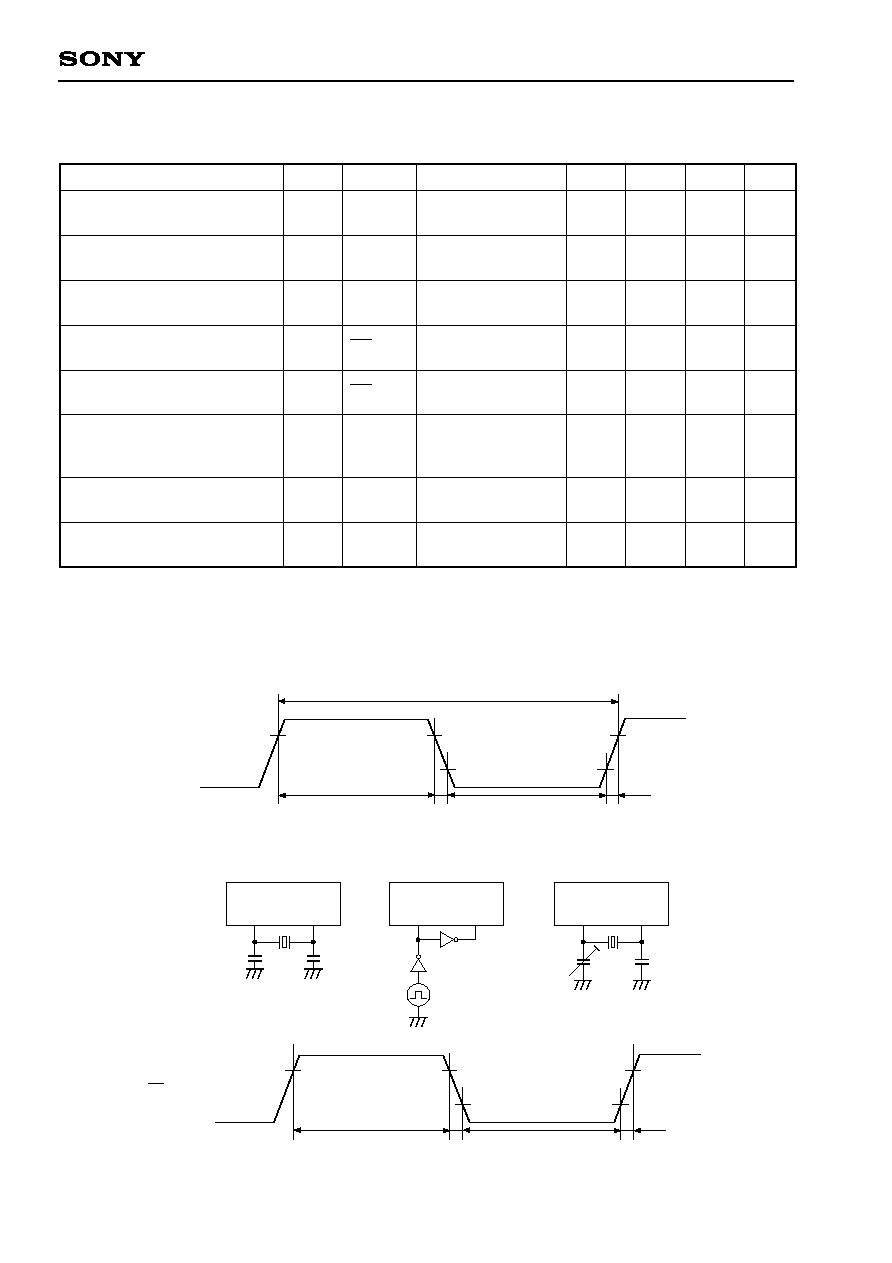
(1) Clock timing
System clock frequency
System clock input pulse width
System clock input rise time,
fall time
Event count input clock
pulse width
Event count input clock
rise time, fall time
System clock frequency
Event count input
pulse width
Event count input rise time,
fall time
f
C
t
XL
t
XH
t
CR
t
CF
t
EH
t
EL
t
ER
t
EF
f
C
t
TL
t
TH
t
TR
t
TF
XTAL
EXTAL
EXTAL
EXTAL
EC
EC
TEX
TX
TEX
TEX
MHz
ns
ns
ns
ms
kHz
µs
ms
Item
Symbol
Pin
Conditions
Min.
Unit
Fig. 1, Fig. 2
Fig. 1, Fig. 2
External clock drive
Fig. 1, Fig. 2
External clock drive
Fig. 3
Fig. 3
V
DD
= 2.7 to 5.5V
Fig. 2 (32kHz clock
applied condition)
Fig. 3
Fig. 3
1
28
4
t
sys
10
Typ.
32.768
Max.
16
200
20
20
(Ta = ≠20 to +75∞C, V
DD
= 4.5 to 5.5V, Vss = 0V reference)
Fig. 2. Clock applied conditions
Fig. 1. Clock timing
Fig. 3. Event count clock timing

≠ 15 ≠
CXP82940/82948/82952/82960
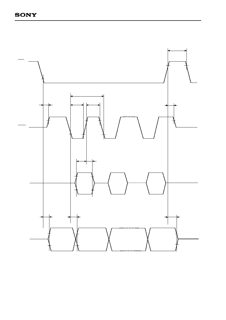
Chip select transfer mode
(SCK = output mode)
Chip select transfer mode
(SCK = output mode)
Chip select transfer mode
Chip select transfer mode
Chip select transfer mode
Note 1)
t
sys indicates the three values below according to the upper two bits (CPU clock selected) of the
control clock registor (address: 00FE
H
).
t
sys (ns) = 2000/fc (upper two bits = "00"), 4000/fc (upper two bits = "01"), 16000/fc (upper two bits = "11")
Note 2) CS, SCK, SI and SO correspond to each pin of CS0, SCK0, SI0 and SO0.
Note 3) The load condition for the SCK output mode, SO output delay time is 50pF + 1TTL.
(2) Serial transfer (CH0)
(Ta = ≠20 to +75∞C, V
DD
= 4.5 to 5.5V, Vss = 0V reference)
Item
CS
SCK
delay time
CS
SCK
float delay time
CS
SO
delay time
CS
SO
float delay time
CS High level width
SCK cycle time
SCK
High, Low level width
SI input setup time
(for SCK
)
SI input hold time
(for SCK
)
SCK
SO
delay time
t
DCSK
t
DCSKF
t
DCSO
t
DCSOF
t
WHCS
t
KCY
t
KH
t
KL
t
SIK
t
KSI
t
KSO
SCK0
SCK0
SO0
SO0
CS0
SCK0
SCK0
SI0
SI0
SO0
Input mode
Output mode
Input mode
Output mode
SCK input mode
SCK output mode
SCK input mode
SCK output mode
SCK input mode
SCK output mode
ns
ns
ns
ns
ns
Symbol
Pin
Min.
1.5
t
sys + 200
1.5
t
sys + 200
1.5
t
sys + 200
1.5
t
sys + 200
t
sys + 200
2
t
sys + 200
8000/fc
t
sys + 100
8000/fc ≠ 100
≠
t
sys + 100
200
2
t
sys + 100
100
ns
ns
ns
ns
ns
ns
ns
ns
ns
ns
2
t
sys + 200
100
Max.
Unit
Condition
≠ 16 ≠
CXP82940/82948/82952/82960
Fig. 4. Serial transfer CH0 timing (CH0)
CSO
SCK0
0.2V
DD
0.8V
DD
t
WHCS
t
DCSK
t
DCSKF
0.8V
DD
0.2V
DD
0.8V
DD
t
KCY
t
KL
t
KH
0.8V
DD
0.2V
DD
SI0
t
SIK
Input data
t
DCSO
t
KSO
t
DCSOF
Output data
0.8V
DD
0.2V
DD
SO0
t
KSI
≠ 17 ≠
CXP82940/82948/82952/82960
Serial transfer (CH1) (SIO mode)
(Ta = ≠20 to +75∞C, V
DD
= 4.5 to 5.5V, Vss = 0V reference)
Item
SCK1 cycle time
t
KCY
SCK1
Input mode
Ouput mode
Input mode
Ouput mode
SCK1 input mode
SCK1 ouput mode
SCK1 input mode
SCK1 ouput mode
SCK1 input mode
SCK1 ouput mode
2
t
sys + 200
16000/fc
t
sys + 100
8000/fc ≠ 50
100
200
t
sys + 200
100
t
sys + 200
100
ns
ns
ns
ns
ns
ns
ns
ns
ns
ns
SCK1
SI1
SI1
SO1
t
KH
t
KL
t
SIK
t
KSI
t
KSO
SCK1
High, Low level width
SI1 input setup time
(for SCK1
)
SI1 input hold time
(for SCK1
)
SCK1
SO1 delay time
Symbol
Pin
Condition
Min.
Max.
Unit
Note 1)
t
sys indicates the three values below according to the upper two bits (CPU clock selected) of the
control clock registor (address: 00FE
H
).
t
sys (ns) = 2000/fc (upper two bits = "00"), 4000/fc (upper two bits = "01"), 16000/fc (upper two bits = "11")
Note 2) The load condition for the SCK1output mode, SO1 output delay time is 50pF + 1TTL.
Fig. 5. Serial transfer CH1 timing (SIO mode)
SCK1
SI1
SO1
t
KCY
t
KL
t
KH
0.2V
DD
0.8V
DD
t
SIK
t
KSI
t
KSO
Input data
Output data
0.2V
DD
0.8V
DD
0.2V
DD
0.8V
DD

≠ 18 ≠
CXP82940/82948/82952/82960
SO1 cycle time
SI1 data setup time
SI1 data hold time
t
LCY
t
LSU
t
LHD
SO1
SI1
SI1
SI1
2
2
104
µs
µs
µs
Item
Symbol
Pin
Condition
Min.
Typ.
Max.
Unit
t
LCY
is specified only when the lower two bits (SO1 clock selected) of the serial mode register (CH1) (SIOM1:
address 01E2
H
) is set to 104µs.
Note) The load condition for SO1 is 50pF + 1TTL.
Serial transfer (CH1) (Special mode)
(Ta = ≠20 to +75∞C, V
DD
= 4.5 to 5.5V, Vss = 0V reference)
Fig. 6. Serial transfer CH1 timing (Special mode)
SO1
SI1
t
LCY
Start bit
Output data bit
t
LCY
0.5V
DD
0.8V
DD
0.2V
DD
t
LCY/2
t
LSU
t
LHD
Input
data bit
≠ 19 ≠
CXP82940/82948/82952/82960
t
CONV
t
SAMP
V
REF
V
IAN
V
ZT
1
V
FT
2
I
REF
AV
REF
AN0 to AN7
Ta = 25∞C
V
DD
= AV
DD
= AV
REF
= 5.0V
V
SS
= AV
SS
= 0V
V
DD
= AV
DD
= 4.5 to 5.5V
AV
REF
I
REFS
µs
µs
V
V
AV
DD
AV
REF
1.0
mA
10
µA
0.6
160/f
ADC
3
12/f
ADC
3
AV
DD
≠ 0.5
0
Bits
8
±3
LSB
70
mV
5030
10
4970
≠10
4910
mV
Fig. 7. Definition of A/D converter terms
Analog input
Linearity error
V
FT
V
ZT
00
H
01
H
FE
H
FF
H
Digital conversion value
00 (
= f
EX
/2)
01 (
= f
EX
/4)
11 (
= f
EX
/16)
f
ADC
= f
C
/2
f
ADC
= f
C
/4
f
ADC
= f
C
/16
0 (
/2 selection)
CKS
PCK1, PCK0
f
ADC
= f
C
f
ADC
= f
C
/2
f
ADC
= f
C
/8
1 (
selection)
Conversion time
Sampling time
Reference input voltage
Analog input voltage
Operation mode
SLEEP mode
STOP mode
32kHz operation mode
Linearity error
Zero transition
voltage
Full-scale
transition voltage
Resolution
AV
REF
current
Item
Symbol
Pin
Condition
Min.
Typ.
Max.
Unit
(3) A/D converter characteristics
(Ta = ≠20 to +75∞C, V
DD
= 4.5 to 5.5V, AV
REF
= 4.0 to AV
DD
, Vss = AV
SS
= 0V reference)
1
V
ZT
: Value at which the digital conversion value change
from 00
H
to 01
H
and vice versa.
2
V
FT
: Value at which the digital conversion value changes
from FE
H
to FF
H
and vice versa.
3
f
ADC
indicates the below values due to the contents of bit 6
(CKS) of the A/D control register (address: 00F9
H
) and bits 7
(PCK1) and 6 (PCK0) of the clock control register (address:
00FE
H
).

≠ 20 ≠
CXP82940/82948/82952/82960
External interruption
High, Low level width
Reset input Low level width
INT0
INT1
INT2
INT3
NMI
RST
1
32/fc
µs
µs
Item
Symbol
Pin
Condition
Min.
Max.
Unit
t
IH
t
IL
t
RSL
(4) Interruption, reset input
(Ta = ≠20 to +75∞C, V
DD
= 4.5 to 5.5V, Vss = 0V reference)
0.2V
DD
0.8V
DD
t
IH
t
IL
INT0
INT1
INT2
INT3
NMI
(NMI specifies only the
falling edge.)
t
IL
t
IH
Fig. 8. Interruption input timing
t
RSL
0.2V
DD
RST
Fig. 9. RST input timing
≠ 21 ≠
CXP82940/82948/82952/82960
(5) I
2
C bus timing
(Ta = ≠20 to +75∞C, V
DD
= 4.5 to 5.5V, Vss = 0V reference)
Item
SCL clock frequency
Bus-free time before starting transfer
Hold time for starting transfer
Clock Low level width
Clock High level width
Setup time for repetitive transfers
Data hold time
Data setup time
SDA, SCL rise time
SDA, SCL fall time
Setup time for transfer completion
f
SLC
t
BUF
t
HD; STA
t
LOW
t
HIGH
t
SU; STA
t
HD; DAT
t
SU; DAT
t
R
t
F
t
SU; STO
SCL
SDA, SCL
SDA, SCL
SCL
SCL
SDA, SCL
SDA, SCL
SDA, SCL
SDA, SCL
SDA, SCL
SDA, SCL
0
4.7
4.0
4.7
4.0
4.7
0
250
4.7
100
1
300
kHz
µs
µs
µs
µs
µs
µs
ns
µs
ns
µs
Symbol
Pin
Condition
Min.
Max.
Unit
The data hold time must exceed 300ns because the SCL rise time (300ns max.) is not taken into consideration.
Fig.10. I
2
C bus transfer timing
P
St
t
SU ; STO
t
SU ; STA
t
HD ; STA
t
SU ; DAT
t
HIGH
t
HD ; DAT
t
F
t
R
t
LOW
t
HD ; STA
S
P
t
BUF
SDA
SCL
Fig.11. Recommended circuit example for I
2
C device
I
2
C
device
I
2
C
device
R
S
R
S
R
S
R
S
R
P
R
P
SDA0
(or SDA1)
SCL0
(or SCL1)
∑ Pull-up resistors (R
P
) must be connected to SDA0 (or SDA1) and SCL0 (or SCL1).
∑ Serial resistance (Rs = 300
or less) of SDA0 (or SDA1) and SCL0 (SCL1) reduces spike noise caused by
CRT flash-over.

≠ 22 ≠
CXP82940/82948/82952/82960
Appendix
Fig. 12. Recommended oscillation circuit
EXTAL
XTAL
C
1
C
2
Rd
(i)
TEX
TX
C
1
C
2
Rd
(ii)
Manufacturer
RIVER
ELETEC
CO., LTD.
KINSEKI
LTD.
Model
HC-49/U03
HC-49/U (-S)
P3
fc (MHz)
8.00
10.00
12.00
8.00
10.00
12.00
12
12
12
12
0
16.00
30
18
470k
(ii)
32.768kHz
10
5
16 (12)
10
16.00
5
16 (12)
16 (12)
16 (12)
0
0
0
C
1
(pF)
C
2
(pF)
Rd (
)
Circuit
example
(i)
(i)
Item
Content
Reset pin pull-up resistance
Non-existent
Existent
Non-existent
Existent (Selectable for each pin)
Mask Option Table
High voltage drive output port pull-down resistance

≠ 23 ≠
CXP82940/82948/82952/82960
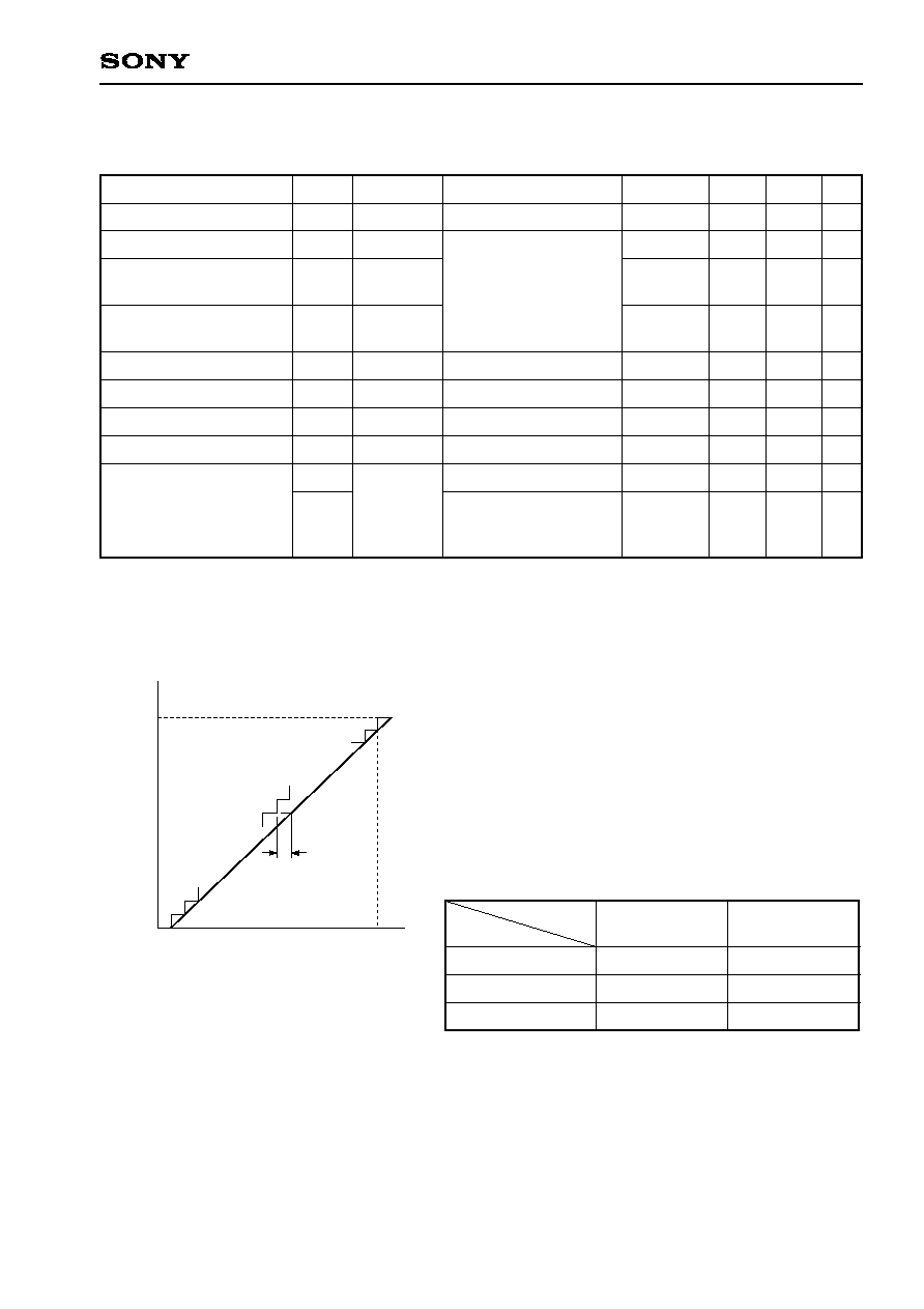
Characteristics Curve
V
DD
≠ Supply voltage [ V ]
I
DD
vs. V
DD
(fc = 16MHz, Ta = 25∞C, Typical)
1/2 dividing mode
1/4 dividing mode
1/16 dividing mode
SLEEP mode
30
20
10
0
2
10
15
3
4
6
5
7
1/2 dividing mode
1/4 dividing mode
1/16 dividing mode
SLEEP mode
32kHz mode
(instruction)
32kHz
SLEEP mode
I
DD
≠ Supply current [mA]
50
30
20
10
5
1
0.5
(500µA)
0.1
(100µA)
0.05
(50µA)
0.01
(10µA)
I
DD
vs. fc
(V
DD
= 5V, Ta = 25∞C, Typical)
5
0
1
Frequency [MHz]
I
DD
≠ Supply current [mA]

≠ 24 ≠
CXP82940/82948/82952/82960
PACKAGE STRUCTURE
SONY CODE
EIAJ CODE
JEDEC CODE
QFP-80P-L01
QFP080-P-1420-A
PACKAGE MATERIAL
LEAD TREATMENT
LEAD MATERIAL
PACKAGE WEIGHT
EPOXY RESIN
SOLDER PLATING
COPPER / 42 ALLOY
1.6g
23.9 ± 0.4
20.0 ≠ 0.1
+ 0.4
1
80
65
64
41
40
25
24
0.8
0.35 ≠ 0.1
+ 0.15
14.0 ≠ 0.1
+ 0.4
17.9 ±
0.4
16.3
0.1 ≠ 0.05
+ 0.2
2.75 ≠ 0.15
+ 0.35
0.8 ±
0.2
0.15 ≠ 0.05
+ 0.1
80PIN QFP (PLASTIC)
M
0.12
0.15
0∞ to 10∞
DETAIL A
A
Package Outline
Unit: mm