≠ 1 ≠
CXP83120A/83124A
E94843A15-PS
CMOS 8-bit Single Chip Microcomputer
Description
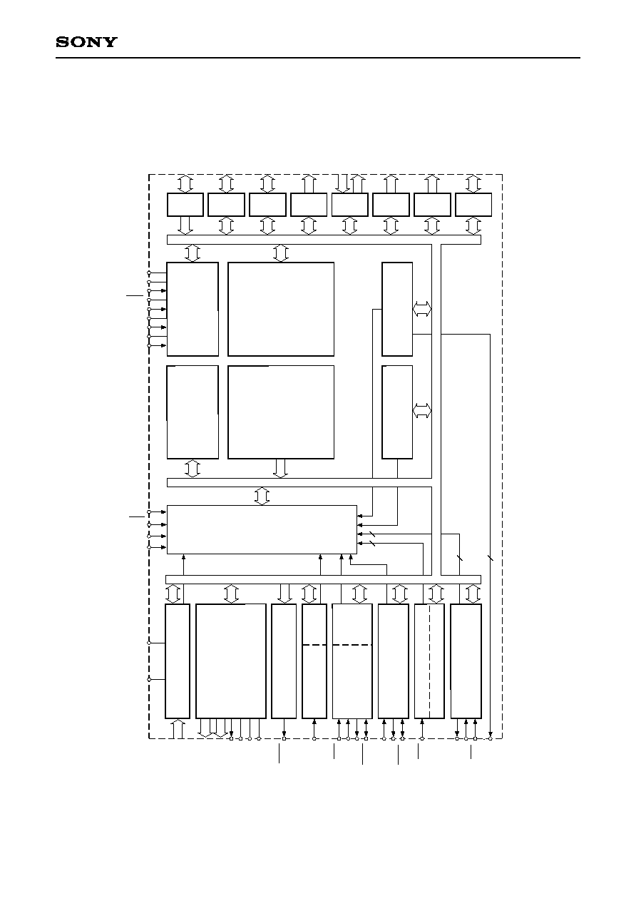
The CXP83120A/83124A is a CMOS 8-bit single
chip microcomputer integrating on a single chip an
A/D converter, serial interface, timer/counter, time
base timer, 32kHz timer/counter, capture timer
counter, LCD controller/driver, remote control
reception circuit and 14-bit PWM output besides the
basic configurations of 8-bit CPU, ROM, RAM, and
I/O port.
The CXP83120A/83124A also provides a sleep/stop
function that enables lower power consumption.
Features
∑ Wide-range instruction system (213 instructions) to cover various types of data.
-- 16-bit arithmetic/multiplication and division/boolean bit operation instructions
∑ Minimum instruction cycle
400ns at 10MHz operation
8µs at 500kHz
122µs at 32kHz operation
∑ Incorporated ROM capacity
20Kbytes (CXP83120A)
24Kbytes (CXP83124A)
∑ Incorporated RAM capacity
644bytes (includes LCD display data area)
∑ Peripheral functions
-- A/D converter
8-bit, 8-channel, successive approximation method
(Conversion time of 32µs/10MHz)
-- Serial interface
8-bit, 8-stage FIFO incorporated
(Auto transfer for 1 to 8 bytes), 1 channel
8-bit clock synchronized type, 1 channel
-- Timer
8-bit timer, 8-bit timer/counter, 19-bit time base timer,
16-bit capture timer/counter, 32kHz timer/counter
-- LCD controller/driver
Maximum 160 segment display possible (during 1/4 duty)
4 common output, 40 segment output
Display method static, 1/2, 1/3, 1/4 duty
Bias method 1/2, 1/3 bias
-- Remote control reception circuit
8-bit pulse measuring counter, 6-stage FIFO
-- PWM output circuit
14 bits, 1 channel
∑ Interruption
15 factors, 15 vectors, multi-interruption possible
∑ Standby mode
SLEEP/STOP
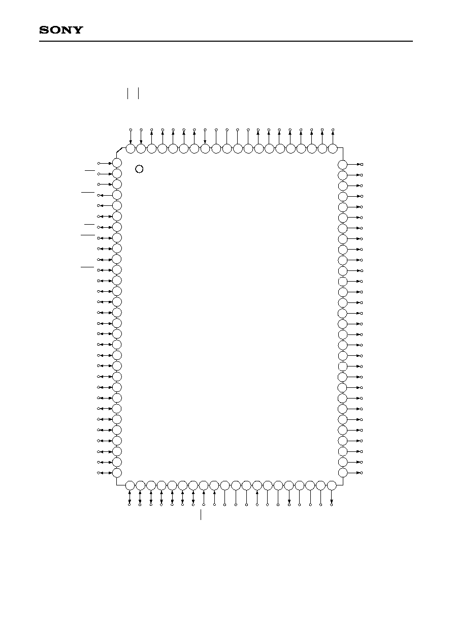
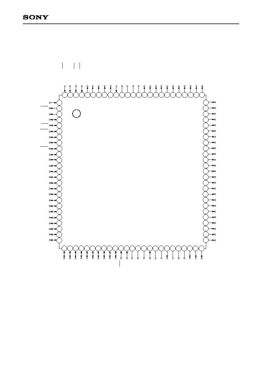
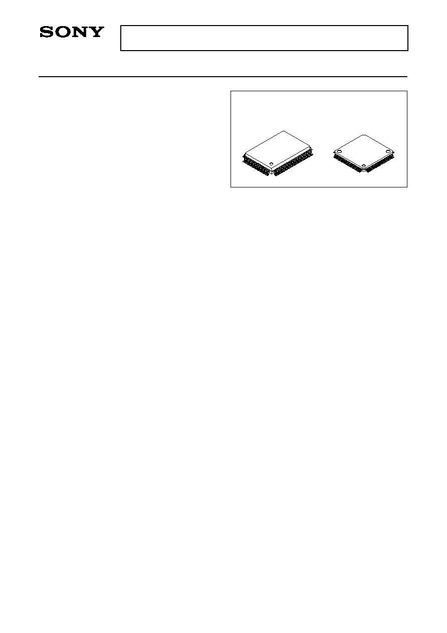
∑ Package
100-pin plastic QFP/LQFP
∑ Piggyback/evaluation chip
CXP83200A 100-pin ceramic QFP/LQFP
Structure
Silicon gate CMOS IC
Sony reserves the right to change products and specifications without prior notice. This information does not convey any license by
any implication or otherwise under any patents or other right. Application circuits shown, if any, are typical examples illustrating the
operation of the devices. Sony cannot assume responsibility for any problems arising out of the use of these circuits.
100 pin QFP (Plastic)
100 pin LQFP (Plastic)
≠ 5 ≠
CXP83120A/83124A
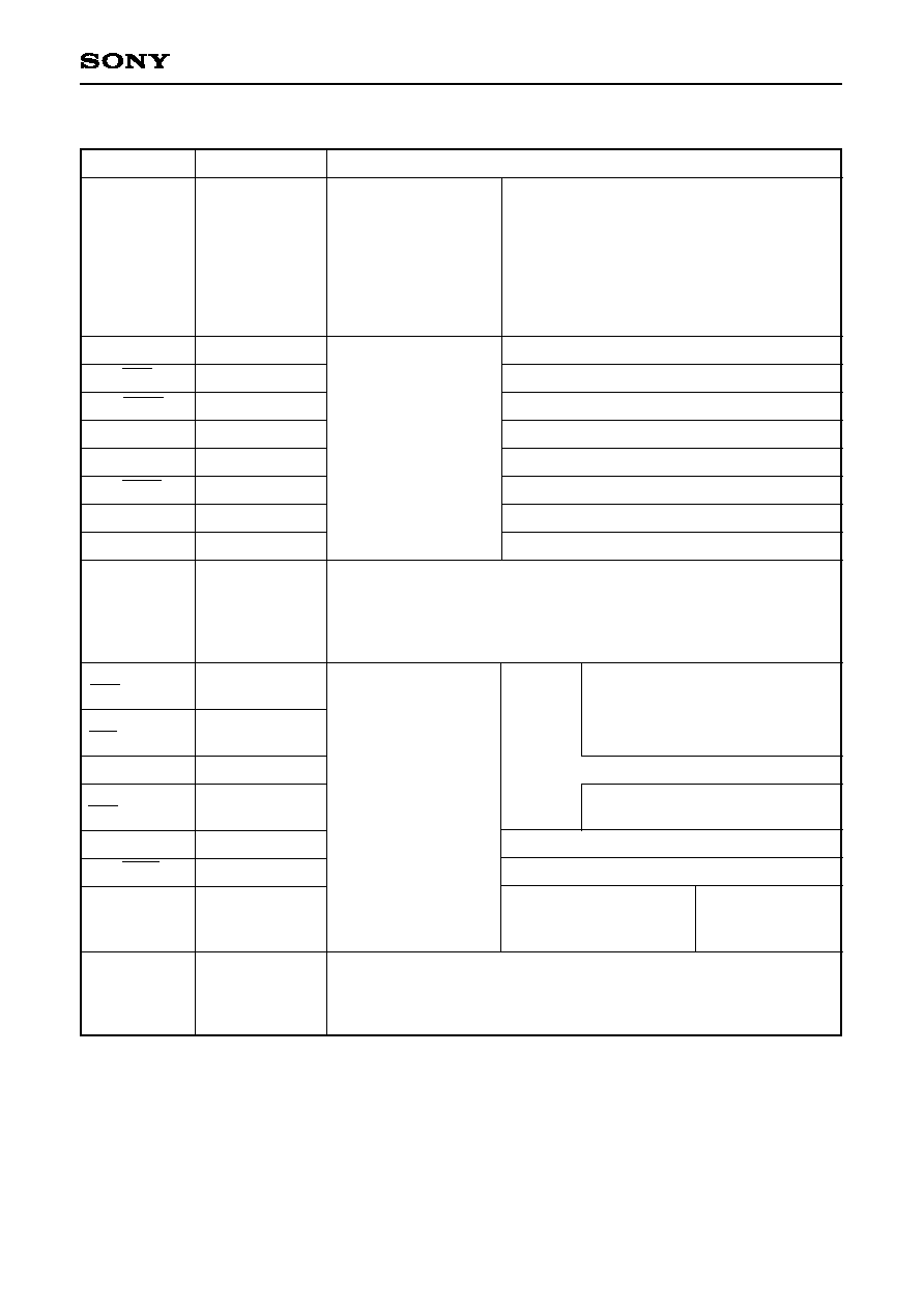
Pin Description
Symbol
I/O
Functions
I/O/Analog input
PA0/AN0
to
PA7/AN7
(Port A)
8-bit I/O port. I/O can
be set in a single bit
unit.
Incorporation of pull-up
resistor can be set
through the software in
a unit of 4 bits. (8 pins)
Analog inputs to A/D converter.
(8 pins)
I/O
PC0 to PC7
PE0/INT0/
EC0
PE1/INT1/
EC1
PE2/INT2
PE3/INT3/
NMI
PE4/RMC
PE5/PWM
PE6/TO/
ADJ
PH0 to PH7
Input/Input/Input
Input/Input/Input
Input/Input
Input/Input/Input
Input/Input
Output/Output
Output/Output/
Output
I/O
(Port C)
8-bit I/O port. I/O can be set in a single bit unit. Capable of driving 12mA
sync current. Incorporation of pull-up resistor can be set through the
software in a unit of 4 bits.
(8 pins)
(Port E)
7-bit port. lower 5 bits
are for inputs; upper 2
bits are for outputs.
(7 pins)
(Port H)
8-bit I/O port. I/O can be set in a single bit unit. Incorporation of pull-up
resistor can be set through the software in a unit of 4 bits.
(8 pins)
External event inputs for
timer/counter.
(2 pins)
External interruption request inputs.
(4 pins)
Non-maskable interruption request
input.
Remote control reception circuit input.
14-bit PWM output.
Rectangular wave output
for 16-bit timer/counter
(duty output 50%).
Output for 32kHz
oscillation
frequency division.
I/O/Input
I/O/Input
I/O/I/O
I/O/Input
I/O/Output
I/O/I/O
I/O/input
I/O/Output
PB0/CINT
PB1/CS0
PB2/SCK0
PB3/SI0
PB4/SO0
PB5/SCK1
PB6/SI1
PB7/SO1
(Port B)
8-bit I/O port. I/O can
be set in a single bit
unit.
Incorporation of pull-up
resistor can be set
through the software in
a unit of 4 bits.
(8 pins)
External capture input to 16-bit timer/counter.
Chip select input for serial interface (CH0).
Serial clock I/O (CH0).
Serial data input (CH0).
Serial data output (CH0).
Serial clock I/O (CH1).
Serial data input (CH1).
Serial data output (CH1).