Description
The CXP84500 is a CMOS 8-bit single chip micro-
computer of piggyback/evaluator combined type,
which is developed for evaluating the function of the
CXP84540/84548.
Features
∑ A wide instruction set (213 instructions) which
covers verious types of data.
≠ 16-bit operation/multiplication and division/Boolean bit operation instructions
∑ Minimum instruction cycle
143ns at 28MHz operation (4.5 to 5.5V)
200ns at 20MHz (3.0 to 5.5V)
∑ Applicable EPROM
LCC type 27C512
(Maximum 60K bytes are available)
∑ Incorporated RAM capacity
1472 bytes
∑ Peripheral functions
≠ A/D converter
8 bits, 8 channels, successive approximation method
(Conversion time of 1.93µs at 28MHz/4.5 to 5.5V, 2.6µs at 20MHz/3.0 to 5.5V)
≠ Serial interface
Incorporated 8-bit, 8-stage FIFO (Auto transfer for 1 to 8 bytes,latch output
function, MSB/LSB first selectable), 1 channel
8-bit clock sync type, 1 channel
≠ Timer
8-bit timer/counter
19-bit time base timer
16-bit capture timer/counter
≠ PWM output
8 bits, 2 channels
∑ Interruption
14 factors, 14 vectors, multi-interruption possible
∑ Standby mode
SLEEP/STOP
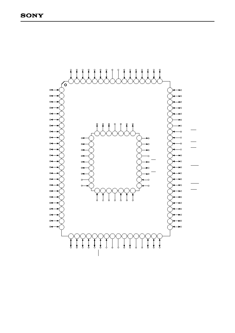
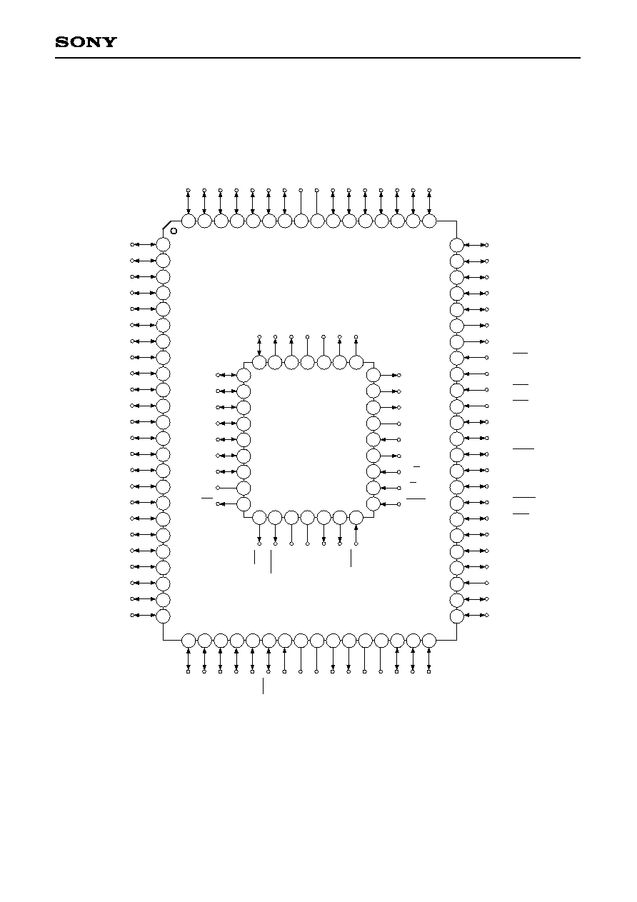
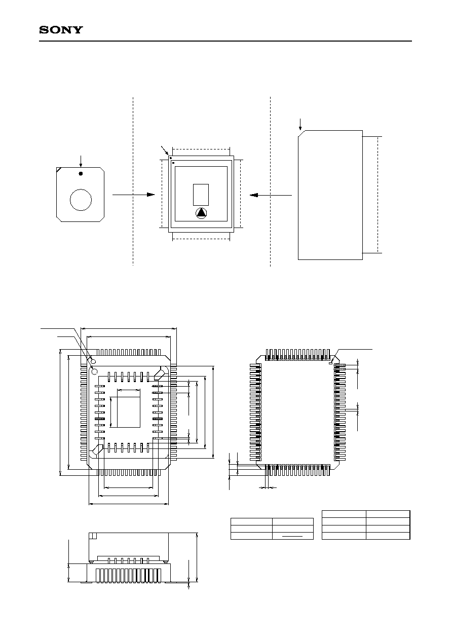
∑ Package
80-pin ceramic PQFP
Note) Mask option depends on the type of the CXP84500. Refer to the Products List for details.
Structure
Silicon CMOS IC
≠ 1 ≠
CXP84500
E96907A82
CMOS 8-bit Single Chip Microcomputer
Sony reserves the right to change products and specifications without prior notice. This information does not convey any license by
any implication or otherwise under any patents or other right. Application circuits shown, if any, are typical examples illustrating the
operation of the devices. Sony cannot assume responsibility for any problems arising out of the use of these circuits.
80 pin PQFP (Ceramic)
Piggyback/
evaluator
≠ 4 ≠
CXP84500
Product List
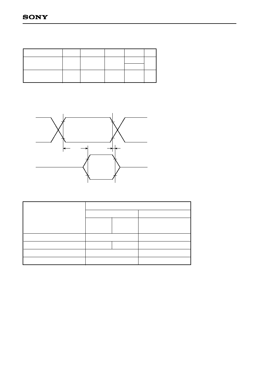
Address
data
input delay time
Address
data
hold time
Item
Symbol
Pin
Min.
Max.
Unit
t
ACC
t
IH
A0 to A15
D0 to D7
A0 to A15
D0 to D7
0
60
1
40
2
ns
ns
t
ACC
t
IH
0.8V
DD
0.8V
DD
0.2V
DD
0.2V
DD
Input data
Address data
A0 to A15
D0 to D7
Products
Mask
Option item
Existent/Non-existent
Existent/Non-existent
Piggyback/evaluator
CXP84500-U01Q
CXP84500-U01R
1
80-pin ceramic PQFP
EPROM 60K bytes
Existent
Existent
2
CXP84540
CXP84548
80-pin plastic QFP
40K bytes
48K bytes
EPROM Read Timing
(Ta = ≠20 to +75∞C, V
DD
= 3.0 to 5.5V, V
SS
= 0V reference)
Package
ROM capacity
Reset pin pull-up resistor
Power-on reset circuit
1
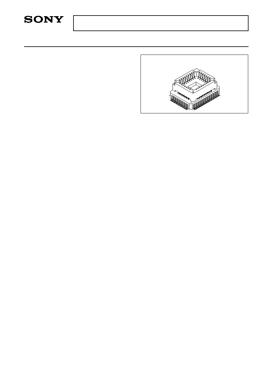
LQFP package conversion adopter used.(SEK-80Q-65MM; attached for piggyback/evaluator)
2
Take the reset time which is more than the oscillation stabilization time by the external reset circuit
because the power-on reset operation cannot be guaranteed for V
DD
= 3.0 to 4.5V.
1
At 20MHz operation (V
DD
= 4.5 to 5.5V). The CXP27C700K is recommended.
2
At 20MHz operation (V
DD
= 3.0 to 5.5V) and 28MHz operation (V
DD
= 4.5 to 5.5V). The CXP27V700K is
recommended.