1
CXP84600
E96707-PS
CMOS 8-bit Single Chip Microcomputer
Description
The CXP84600 is a CMOS 8-bit single chip micro-
computer of piggyback/evaluator combined type,
which is developed for evaluating the function of the
CXP84632/84640/84648.
Features
· A wide instruction set (213 instructions) which covers
various types of data
-- 16-bit operation/multiplication and division/
Boolean bit operation instructions
· Minimum instruction cycle
250ns at 16MHz operation (4.5 to 5.5V)
333ns at 12MHz operation (3.0 to 5.5V)
122µs at 32kHz operation (2.7 to 5.5V)
· Applicable EPROM
LCC type 27C512 (Maximum 60K bytes are available.)
· Incorporated RAM capacity
2048 bytes
· Peripheral functions
-- A/D converter
8 bits, 8 channels, successive approximation method
(Conversion time of 20µs at 16MHz)
-- Serial interface
Srart-stop synchronization (UART), 1 channel
Incorporated buffer RAM (Auto transfer for 1 to 32 bytes), 1 channel
Incorporated 8-bit, 10-stage FIFO
(Auto transfer for 1 to 10 bytes), 1 channel
8-bit clock synctype (MSB/LSB first selectable), 1 channel
-- Timer
8-bit timer, 8-bit timer/counter, 19-bit time base timer,
16-bit capture timer/counter, 32kHz timer/counter
-- I
2
C bus interface
-- Remote control reception circuit
8-bit pulse measurement counter, 6-stage FIFO
-- PWM output circuit
12 bits, 2 channels
· Interruption
21 factors, 15 vectors, multi-interruption possible
· Standby mode
SLEEP/STOP
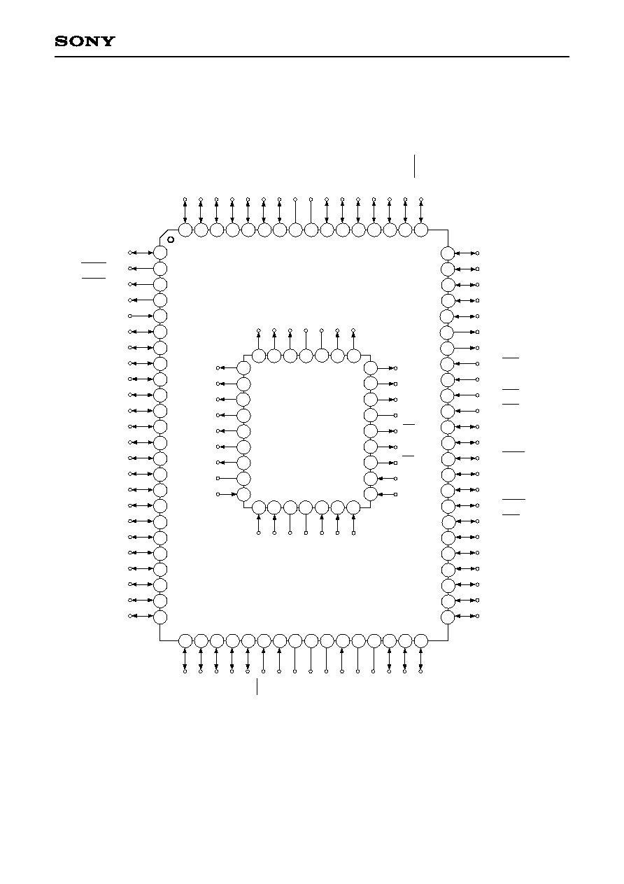
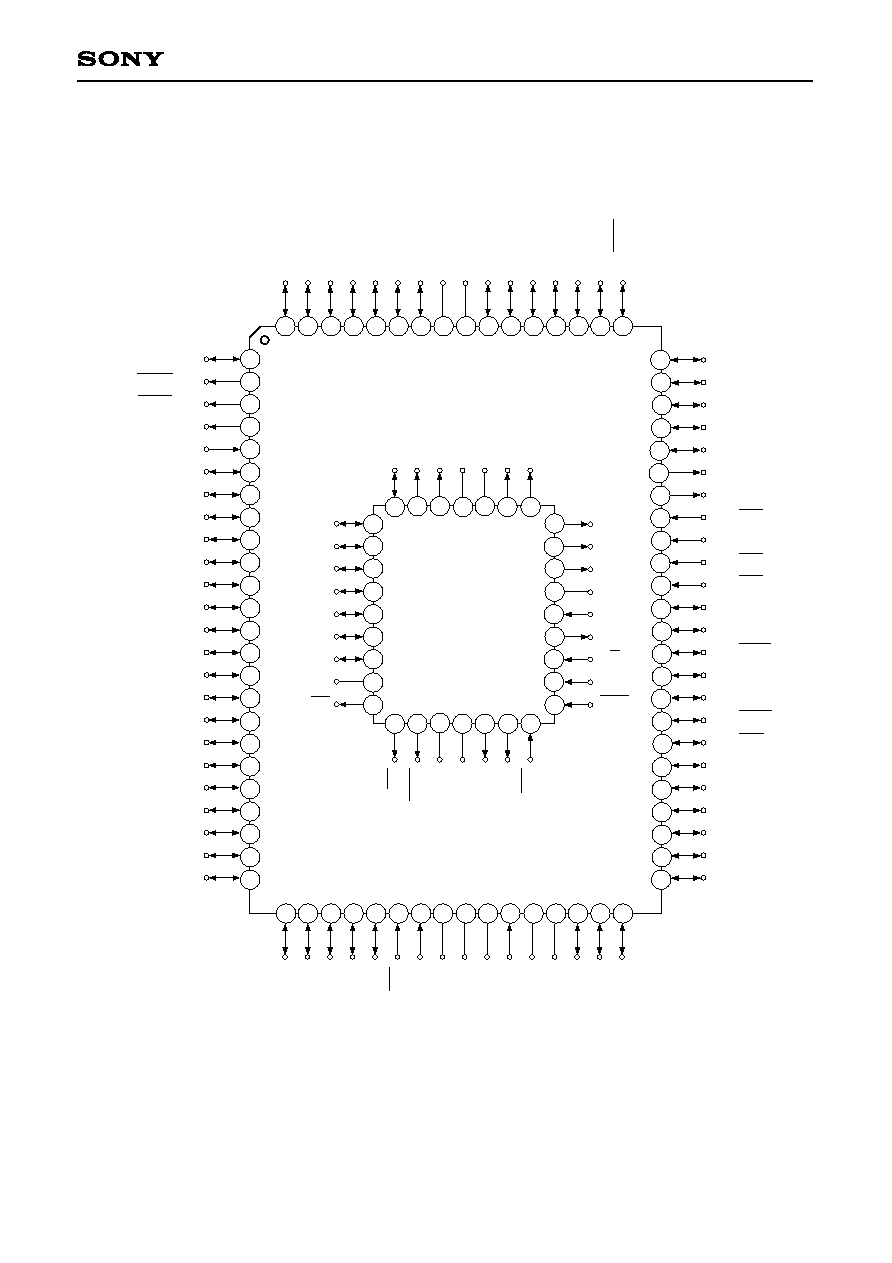
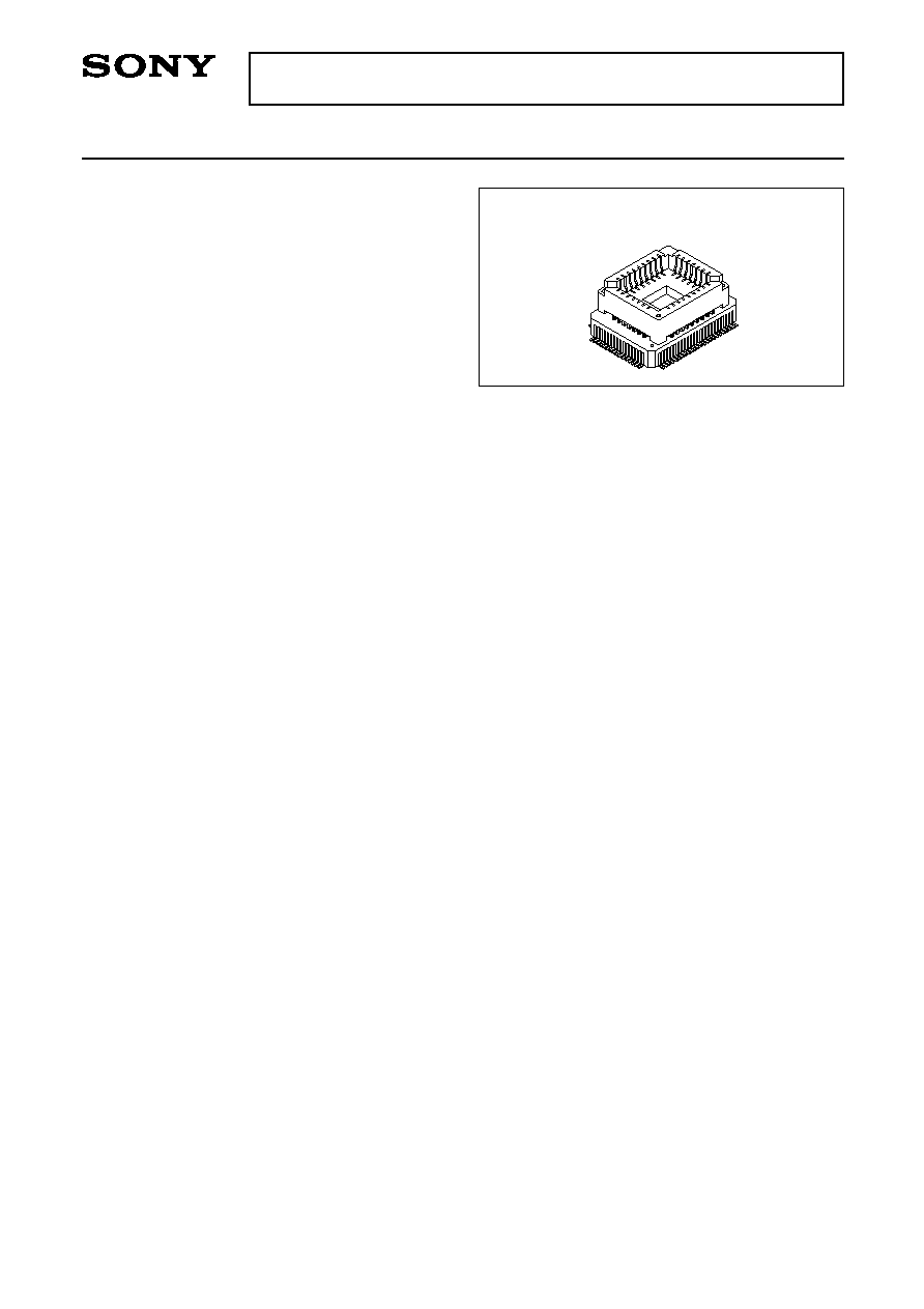
· Package
80-pin ceramic PQFP
Note) Mask option depends on the type of the CXP84600. Refer to the Products List for details.
Structure
Silicon gate CMOS IC
Perchase of Sony's I
2
C components conveys a licence under the Philips I
2
C Patent Rights to use these components
in an I
2
C system, provided that the system conforms to the I
2
C Standard Specifications as defined by Philips.
Sony reserves the right to change products and specifications without prior notice. This information does not convey any license by
any implication or otherwise under any patents or other right. Application circuits shown, if any, are typical examples illustrating the
operation of the devices. Sony cannot assume responsibility for any problems arising out of the use of these circuits.
80 pin PQFP (Ceramic)
Piggyback/
evaluator type
4
CXP84600
100
1
75
2
EPROM Read Timing (Ta = 20 to +75°C, V
DD
= 3.0 to 5.5V, Vss = 0V reference)
Address
data
hold time
Address
data
input delay time
Item
Symbol
Pin
Min.
Max.
Unit
t
IH
t
ACC
A0 to A15
D0 to D7
A0 to A15
D0 to D7
0
ns
ns
t
ACC
t
IH
0.8V
DD
0.8V
DD
0.2V
DD
0.2V
DD
Input data
Address data
A0 to A15
D0 to D7
1
At 12MHz operation (V
DD
= 4.5 to 5.5V)
2
At 12MHz operation (V
DD
= 3.0 to 5.5V), At 16MHz operation (V
DD
= 4.5 to 5.5V)
Products List
Products
Mask
Option item
Existent/Non-existent
Piggyback/evaluator
CXP84600-U01Q
80-pin ceramic QFP
EPROM 60K bytes
Existent
CXP84632 CXP84640 CXP84648
80-pin plastic QFP
32K bytes 40K bytes 48K bytes
Package
ROM capacity
Reset pin pull-up resistor