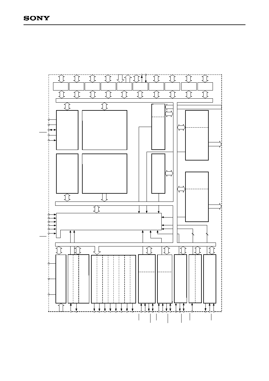
Description
The CXP847P60 is a CMOS 8-bit single chip
microcomputer integrating on a single chip an A/D
converter, serial interface, timer/counter, time base
timer, capture timer/counter, FRC capture unit, high-
precision timing pattern generation circuit, PWM
output, and the like besides the basic configurations
of 8-bit CPU, PROM, RAM, and I/O ports.
The CXP847P60 also provides the sleep/stop
functions that enable to execute the power-on reset
function and lower the power consumption.
The CXP847P60 is the PROM-incorporated version
of the CXP84716/84720/84724 with built-in mask
ROM. This provides the additional feature of being
able to write directly into the program. Thus, it is
most suitable for evaluaiton use during system
development and for small-quantity production.
Features
∑ A wide instruction set (213 instructions) which covers various types of data.
-- 16-bit arithmetic/multiplication and division/Boolean bit operation instructions
∑ Minimum instruction cycle
250ns at 16MHz operation (4.5 to 5.5V)
333ns at 12MHz operation (3.0 to 5.5V)
∑ Incorporated PROM capacity
60K bytes
∑ Incorporated RAM capacity
2144 bytes
∑ Peripheral functions
-- A/D converter
8 bits, 8 channels, successive approximation method
(Conversion time of 1.6µs at 16MHz)
-- Serial interface
Srart-stop synchronization (UART), 1 channel
Incorporated buffer RAM (Auto transfer for 1 to 32 bytes), 2 channels
8-bit clock syncronization (MSB/LSB first selectable), 1 channel
-- Timer
8-bit timer, 8-bit timer/counter, 19-bit time base timer,
16-bit capture timer/counter
-- FRC capture unit
Incorporated 24-bit and 6-stage FIFO
-- High-precision timing pattern generation circuit
PPG: maximum of 11 pins, 16 stages programmable, 2 channels
-- PWM output
8 bits, 8 channels
∑ Interruption
19 factors, 15 vectors, multi-interruption possible
∑ Standby mode
Sleep/stop
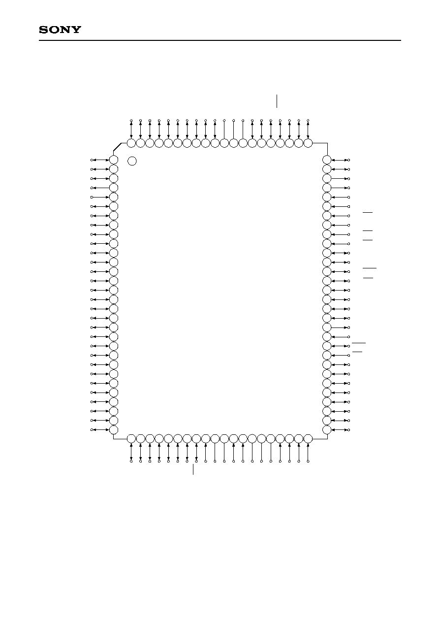
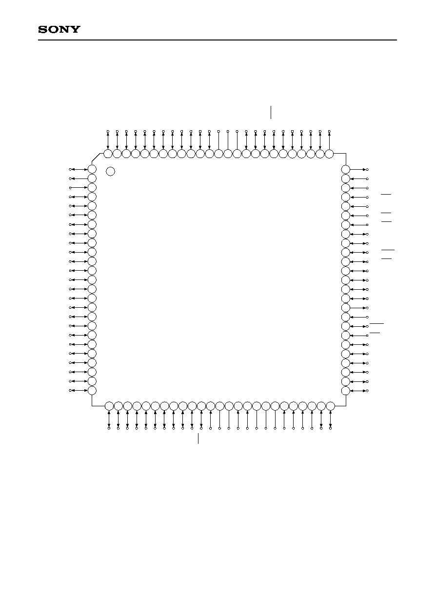
∑ Package
100-pin plastic QFP/LQFP
Structure
Silicon gate CMOS IC
≠ 1 ≠
CXP847P60
E97119A1X-PS
CMOS 8-bit Single Chip Microcomputer
Sony reserves the right to change products and specifications without prior notice. This information does not convey any license by
any implication or otherwise under any patents or other right. Application circuits shown, if any, are typical examples illustrating the
operation of the devices. Sony cannot assume responsibility for any problems arising out of the use of these circuits.
100 pin QFP (Plastic)
100 pin LQFP (Plastic)

≠ 5 ≠
CXP847P60
Analog inputs to A/D converter.
(4 pins)
(Port A)
8-bit I/O port. I/O can be set in
a unit of single bits.
Incorporation of pull-up
resistor can be set through the
software in a unit of 4 bits.
(8 pins)
(Port B)
8-bit I/O port. I/O can be set in
a unit of single bits.
Incorporation of pull-up resistor
can be set through the
software in a unit of 4 bits.
(8 pins)
(Port C)
8-bit I/O port. I/O can be set in a unit of single bits. Can drive 12mA sink
current. Incorporation of pull-up resistor can be set through the software in
a unit of 4 bits.
(8 pins)
(Port D)
8-bit I/O port. I/O can be set in
a unit of single bits.
Incorporation of pull-up resistor
can be set through the software
in a unit of 4 bits.
Data is gated with PPO contents
by OR-gate and they are output.
(8 pins)
(Port E)
8-bit port. Lower 6 bits are for
input; upper 2 bits are for
output.
(8 pins)
Pin Description
AN0
to
AN3
PA0/AN4
to
PA3/AN7
PA4 to PA7
PB0/CINT
PB1 to PB3
PB4/CS1
PB5/SCK1
PB6/SI1
PB7/SO1
PC0 to PC7
PD0/PPO0
to
PD7/PPO7
PE0/EC0
PE1/EC1
PE2
PE3/NMI
PE4 to PE5
PE6
PE7/TO
Input
I/O/Input
I/O
I/O/Input
I/O
I/O/Input
I/O/I/O
I/O/Input
I/O/Output
I/O
I/O/Real-time
output
Input/Input
Input/Input
Input
Input/Input
Input
Output
Output/Output
Analog inputs to A/D converter.
(4 pins)
External capture input to 16-bit
timer/counter.
Chip select input for serial interface
(CH1).
Serial clock I/O (CH1).
Serial data input (CH1).
Serial data output (CH1).
PPO0 to PPO7 outputs for programmable
pattern generator (PPG0). Functions as
high-precision real-time pulse output port.
(PPG0: 11 pins; PPG1: 11 pins)
External event inputs for timer/counter.
(2 pins)
Non-maskable interruption request.
Rectangular wave output for 16-bit
timer/counter.
Symbol
I/O
Description