1
CXP851P16
E94332A18-PS
CMOS 8-bit Single Chip Microcomputer
Sony reserves the right to change products and specifications without prior notice. This information does not convey any license by
any implication or otherwise under any patents or other right. Application circuits shown, if any, are typical examples illustrating the
operation of the devices. Sony cannot assume responsibility for any problems arising out of the use of these circuits.
64 pin SDIP (Plastic)
64 pin QFP (Plastic)
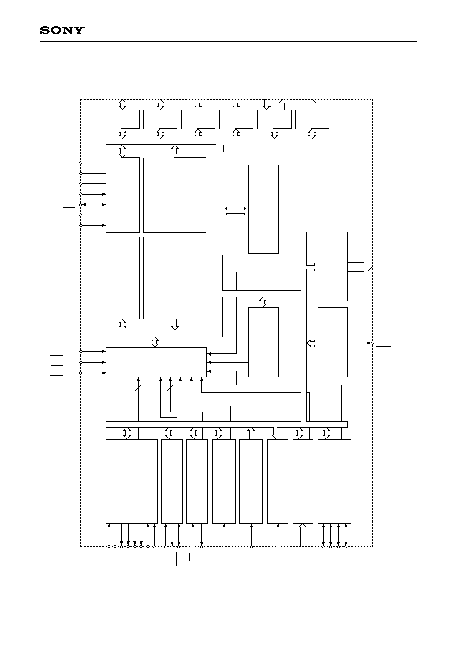
Description
The CXP851P16 are highly integrated micro-
computers composed of a 8-bit CPU, PROM, RAM,
and I/O ports. These chips feature many other high-
performance circuits in a single-chip CMOS design,
including an A/D converter, serial interface,
timer/counter, time-base timer, vector interrupt, on-
screen display function, I
2
C bus interface, PWM
generator, remote control receiver, HSYNC counter,
power supply frequency counter, and watchdog
timer.
Also this IC provides power-on reset and sleep
functions. The designers have ensured low power
consumption for these powerful microcomputers.
The CXP851P16 is the on-chip PROM version of
the CXP85116 with on-chip mask ROM, providing
the function of being able to write directly into the
program. Furthermore, because of the OSD
character ROM can also be written directly into, it is
suitable for evaluation use during system
development and for small quantity production.
Structure
Silicon gate CMOS IC
Features
· A wide instruction set (213 instructions) which cover various types of data.
-- 16-bit arithmetic instruction/multiplication and division instructions/boolean bit operation instruction
· Minimum instruction cycle
During operation 1µs/4MHz
· Incorporated PROM capacity
16K bytes (For program)
3K bytes (For OSD)
· Incorporated RAM capacity
352 bytes
· Peripheral functions
-- On-screen display function
12
×
16 dots, 128 types
4 lines of 21 characters (5 or more lines possible)
double scanning mode supported includes jitter elimination circuit
-- I
2
C bus interface
-- PWM output
14-bits, 1 channel
6-bits, 8 channels
-- Remote control receiving circuit
8-bit pulse measuring counter, 6-stage FIFO
-- A/D converter
4-bit, 4-channel, successive approximation method
(conversion time of 40µs/4MHz)
-- HSYNC counter
-- Power supply frequency counter
-- Watchdog timer
-- 8-bit synchronized serial I/O
-- 8-bit timer, 8-bit timer/counter, 19-bit time-base timer
· Interruption
14 factors, 14 vectors, multiple interrupt possible
· Standby mode
SLEEP/STOP
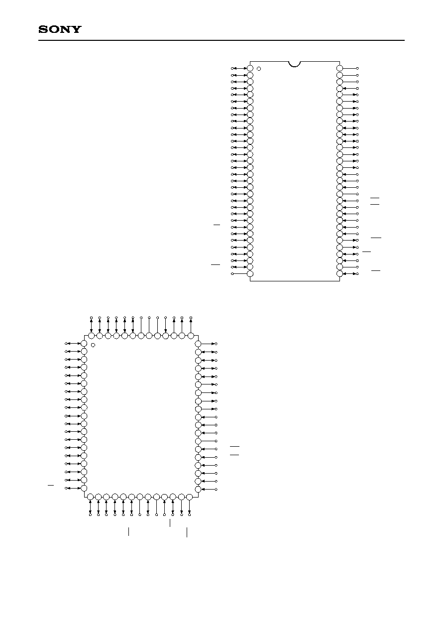
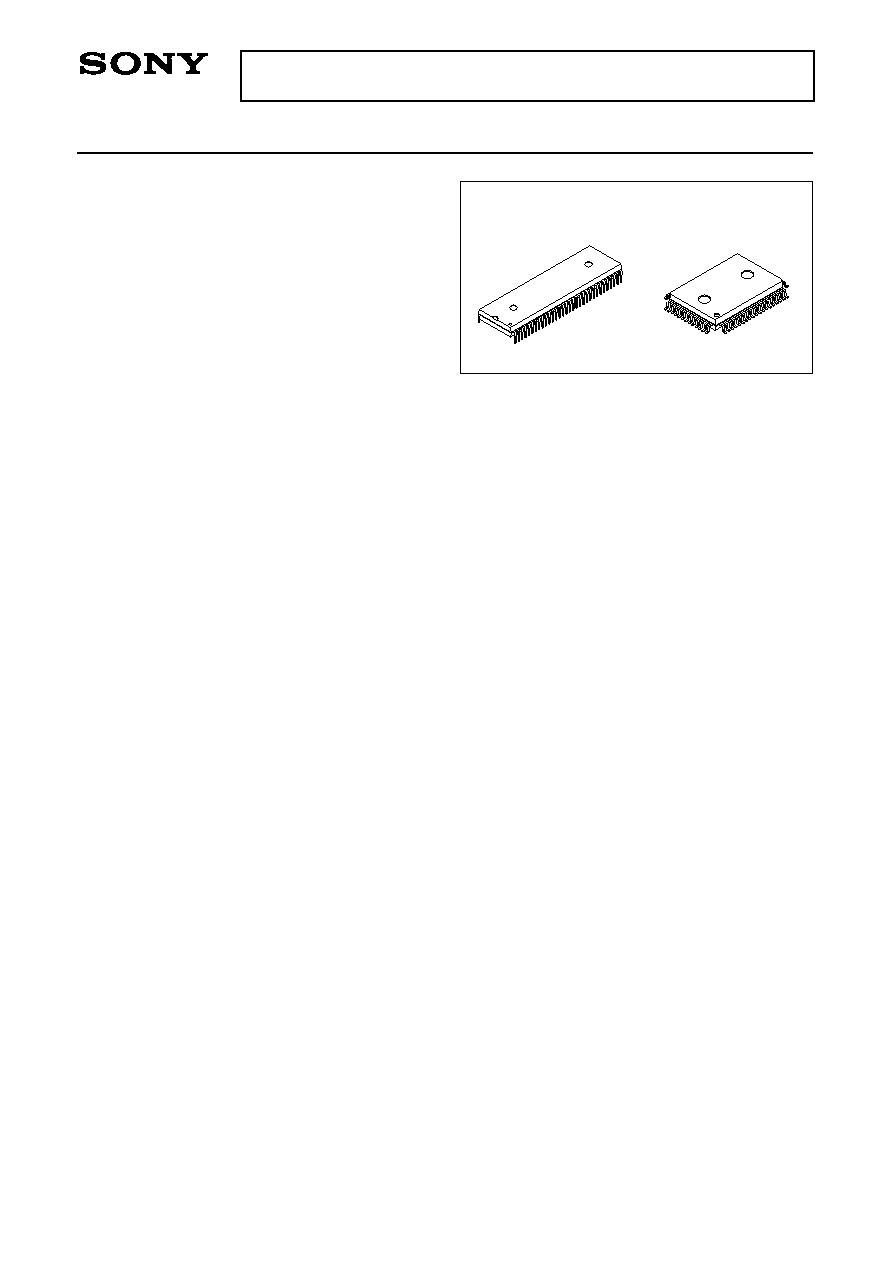
· Package
64-pin plastic SDIP/QFP
Perchase of Sony's I
2
C components conveys a licence under the Philips I
2
C Patent Rights to use these components
in an I
2
C system, provided that the system conforms to the I
2
C Standard Specifications as defined by Philips.
4
CXP851P16
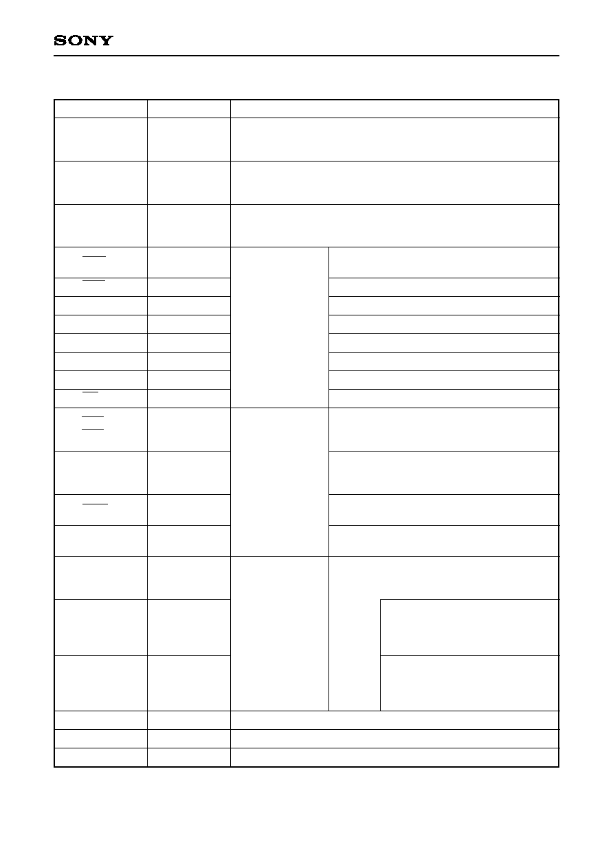
(Port A)
Single bit selectable 8-bit port.
(8 lines)
(Port B)
Single bit selectable 8-bit port.
(8 lines)
(Port C)
Single bit selectable 8-bit port.
(8 lines)
(Port D)
Single bit selectable
8-bit port.
12mA sink current
drive possible.
(8 lines)
(Port E)
8-bit port, lower
6 bits for input,
upper 2 bits for
output.
(8 lines)
(Port F)
8-bit output port
with large current
(12mA) N-ch open
drain output.
Lower 4 bits
middle voltage
tolerance (12V),
upper 4 bits 5V
suppression.
(8 lines)
CRT display 4-bit output pin.
CRT display horizontal synchronization signal input pin.
CRT display vertical synchronization signal input pin.
Pin Description
Symbol
PA0 to PA7
PB0 to PB7
PC0 to PC7
PD0/INT2
PD1/SCK
PD2/SO
PD3/SI
PD4/HSI
PD5/ACI
PD6/RMC
PD7/EC
PE0/INT0
PE1/INT1
PE2/AN0
to
PE5/AN3
PE6/PWM
PE7/TO
PF0/PWM0
to
PF3/PWM3
PF4/PWM4/
SCL0
PF5/PWM5/
SCL1
PF6/PWM6/
SDA0
PF7/PWM7/
SDA1
R, G, B, BLK
HSYNC
VSYNC
I/O
I/O
I/O
I/O/Input
I/O/I/O
I/O/Output
I/O/Input
I/O/Input
I/O/Input
I/O/Input
I/O/Input
Input/Input
Input/Input
Output/Output
Output/Output
Output/Output
Output/Output/
I/O
Output/Output/
I/O
Output
Input
Input
I/O
Description
Input pin for external interrupt request.
Active on falling edge.
Serial clock pin.
Serial data output pin.
Serial data input pin.
HSYNC counter input pin.
Power supply frequency counter input pin.
Remote control receiver circuit input pin.
External event timer/counter input pin.
Input pin for external interrupt request.
Active on falling edge.
(2 lines)
Analog input pin for A/D converter.
(4 lines)
14-bit PWM output pin.
(CMOS output)
Square wave output for timer 1.
(50% duty cycle)
6-bit PWM output pin.
(8 lines)
I
2
C bus interface transfer clock
input/output pin.
I
2
C bus interface transfer data
input/output pin.
5
CXP851P16
Symbol
EXLC
XLC
EXTAL
XTAL
RST
MP
V
DD
Vpp
Vss
Input
Output
Input
Output
I/O
Input
CRT display clock oscillator input/output pin.
Oscillator frequency is determined by external L, C circuit.
System clock oscillator crystal connection pin. When using an external
clock, input to EXTAL pin and leave XTAL pin open.
"L" level active system reset. This pin also acts as an input/output pin
during power up. While internal power-on reset function is taking place
a "L" level is output. (Mask option)
Microprocessor mode input pin. Must be connected to GND.
Positive power supply pin.
Positive power supply pin for on-chip PROM writing.
Please connect to V
DD
for normal operation.
GND. Both Vss pins should be connected to common GND.
I/O
Description