ChipFind - документация

Электронный компонент: CXP85300A-U03Q

Скачать:  PDF   ZIP
/home/web/doc/html/sony/169185
background image
CMOS 8-bit 1-chip Microcomputer
Description
The CXP85300A/85390A are CMOS 8-bit 1-chip
microcomputers that serve as both piggyback and
evaluator. The CXP85300A/85390A are developed
for evaluating the function of the CXP85324A/CXP
85332A/85340A.
Note that CXP85300A corresponds to the fixed
font, and CXP85390A corresponds to the custom
font respectively.
Features
Instruction set which supports a wide array of data
types
-- 213 types of instructions which include 16-bit
calculations, multiplication and division arithmetic,
and boolean bit operations.
Minimum instruction cycle 1s/4MHz (4MHz version)
0.5s/8MHz (8MHz version)
EPROM
27C512
LCC type 27C512
Incorporated RAM capacity
576 bytes
EPROM for custom font (CXP85390A only)
LCC type 27C256, LCC type 27C512
(used volume is 16K bytes)
Peripheral functions
-- On-screen display function
12
18 dots, 256 types 15 colors, 21 characters
12 lines
Black frame output half blanking, shadow, background color on full screen/
half blanking
Double scanning mode, jitter elimination circuit
-- I
2
C bus interface
-- PWM output
14 bits, 1 channel
8 bits, 8 channels
-- Remote control receiving circuit 8-bit pulse measurement counter, 6-stage FIFO
-- A/D converter
8 bits, 4 channels, successive approximation system
(conversion time of 40s/4MHz, 8MHz)
-- HSYNC counter
-- Power supply frequency counter
-- Watchdog timer
-- Serial I/O
8-bit clock synchronized
-- Timers
8-bit timer, 8-bit timer/counter, 19-bit time-base timer
Interrupts
14 factors, 14 vectors multi-interruption possible
Standby mode
Sleep
Package
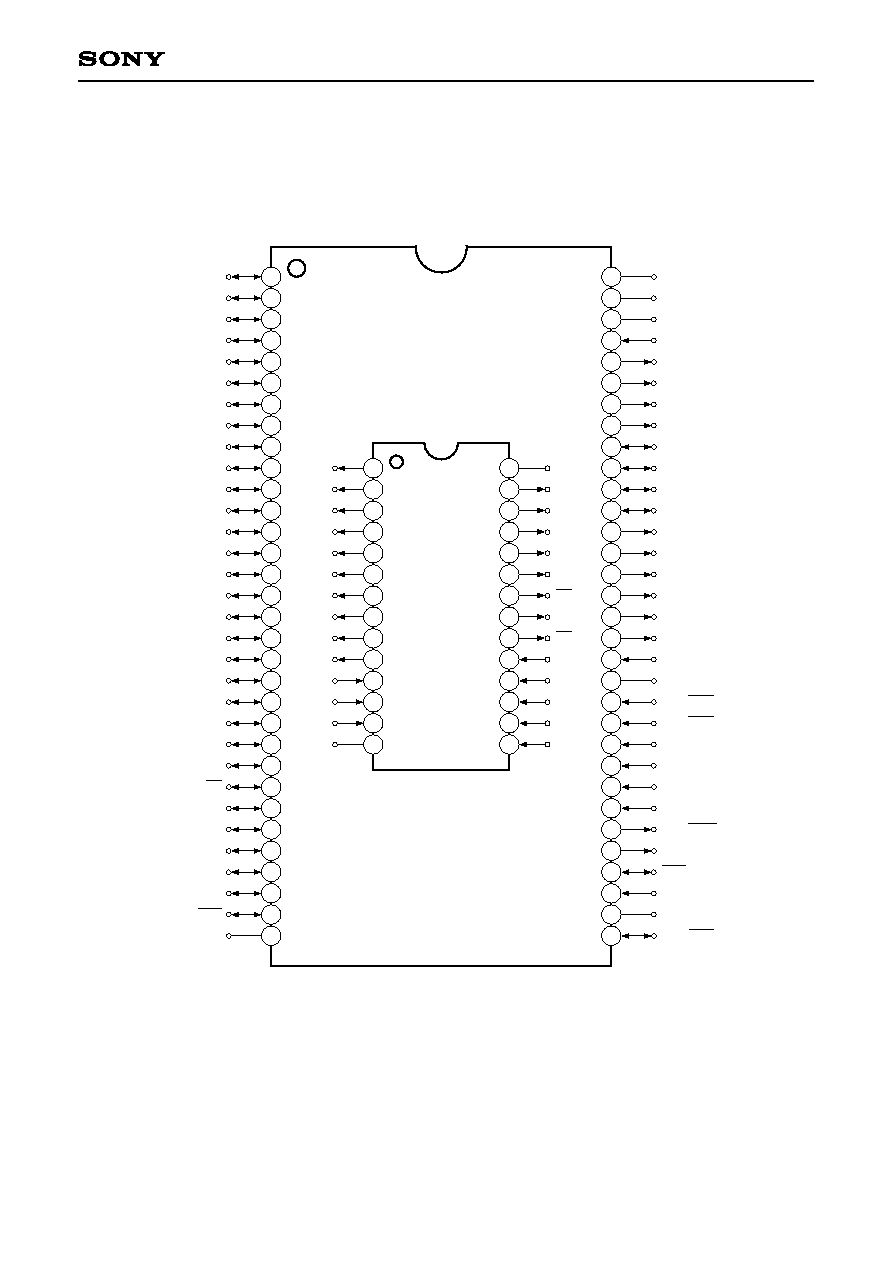
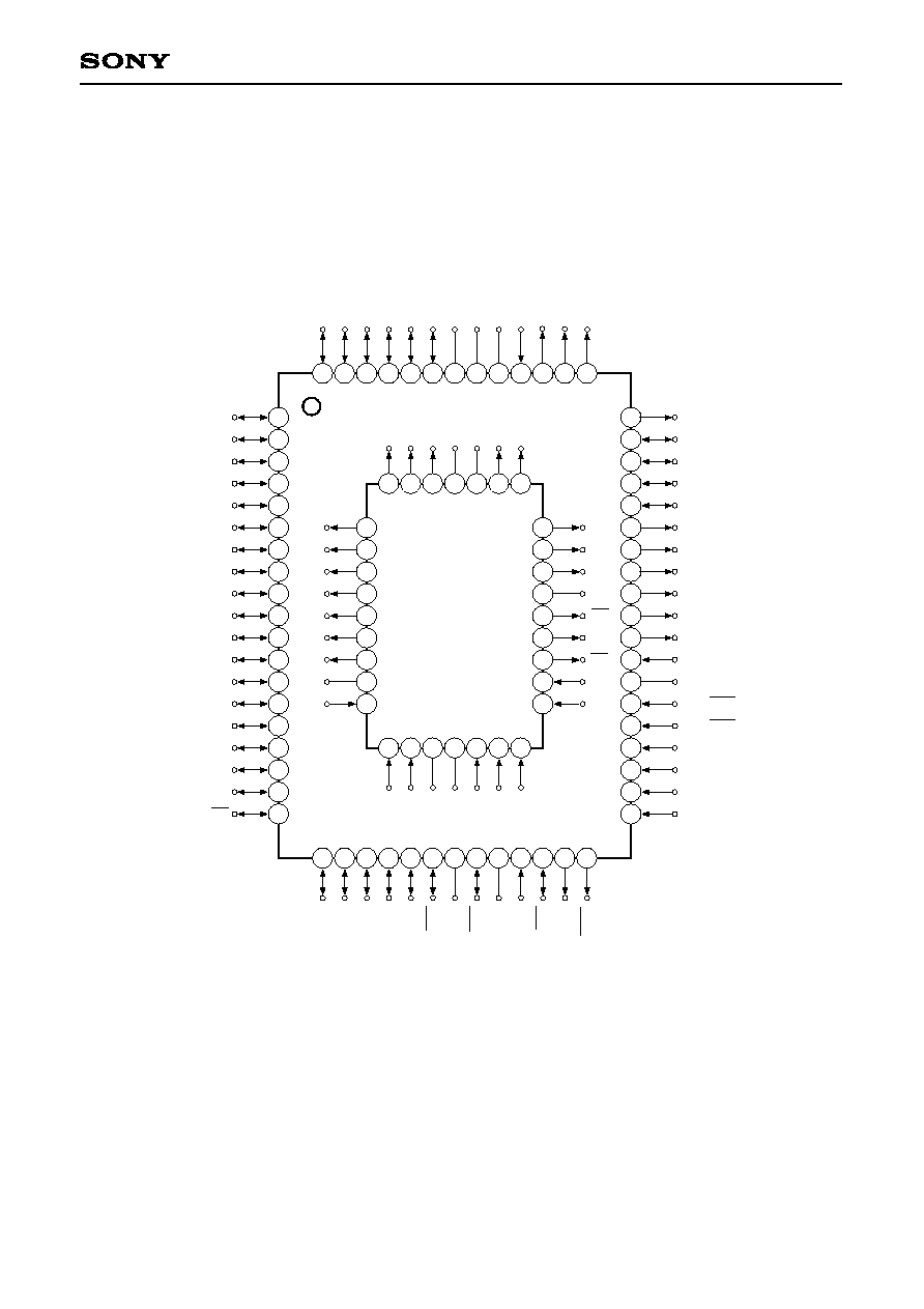
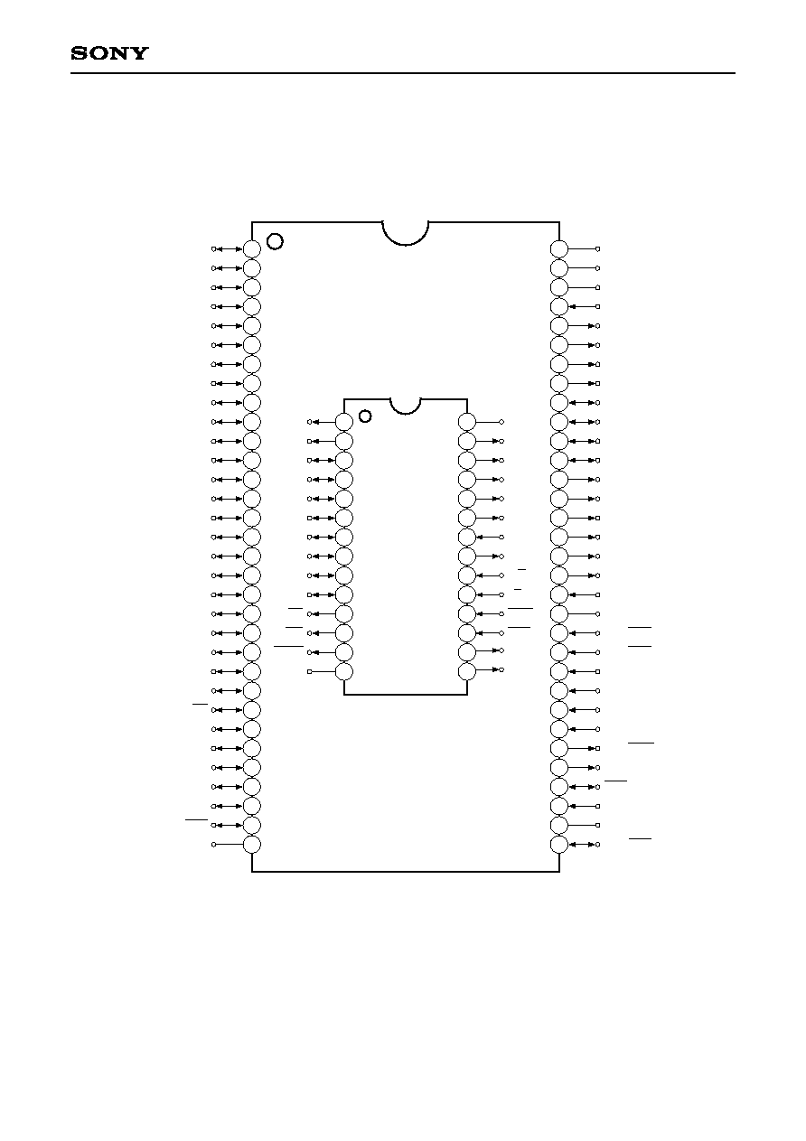
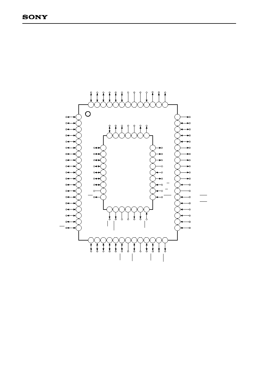
64-pin ceramic SDIP/QFP
Structure
Silicon gate CMOS IC
Note) Optional mask depends on the type of the CXP85300A/85390A. Refer to the product list for details.
1
E94334A7Z-PS
Sony reserves the right to change products and specifications without prior notice. This information does not convey any license by
any implication or otherwise under any patents or other right. Application circuits shown, if any, are typical examples illustrating the
operation of the devices. Sony cannot assume responsibility for any problems arising out of the use of these circuits.
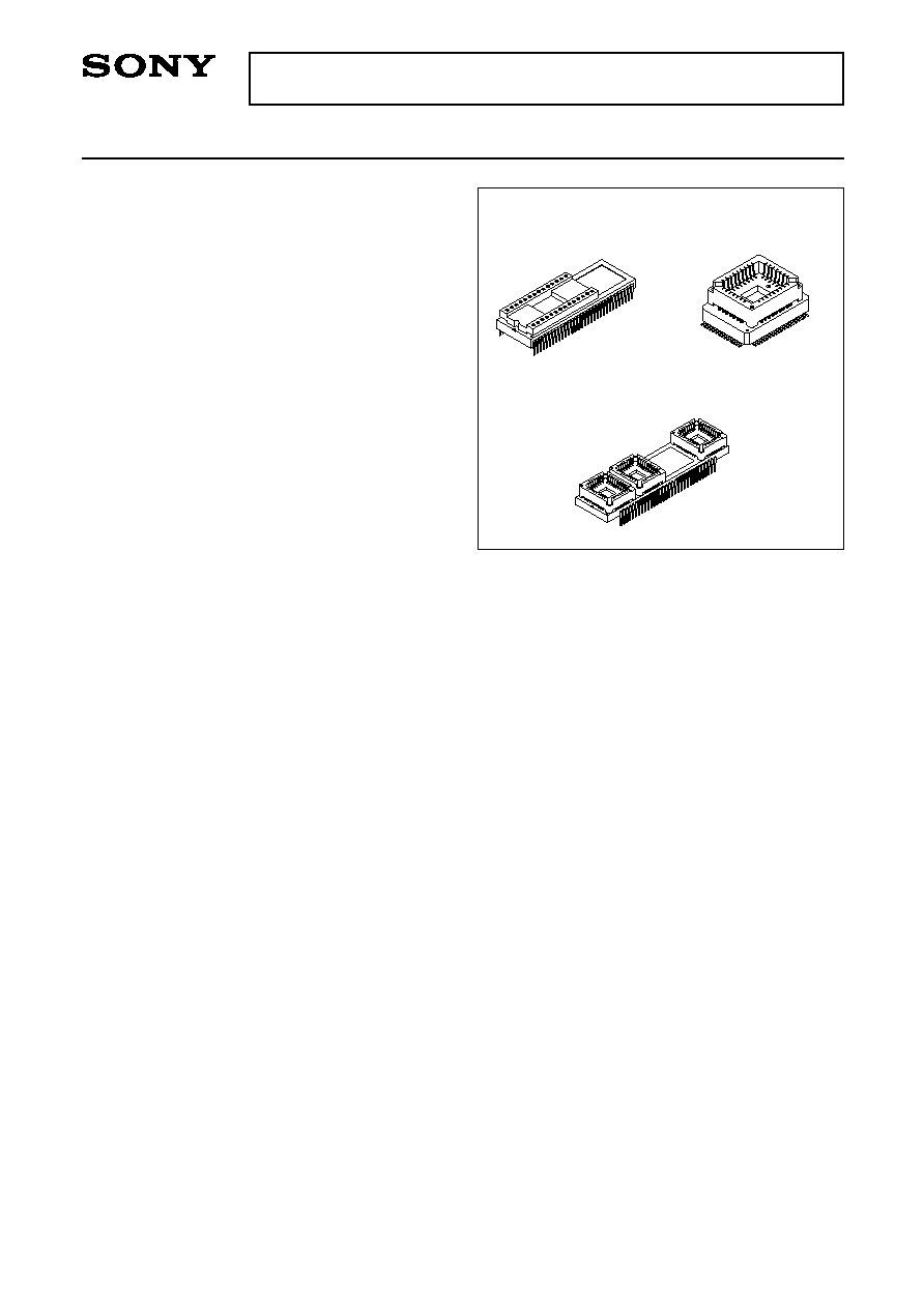
CXP85300A/85390A
64 pin PSDIP (Ceramic)
64 pin PQFP (Ceramic)
Piggyback/
evaluator type
Purchase of Sony's I
2
C components conveys a license under the Philips I
2
C Patent Rights to use these components
in an I
2
C system, provided that the system conforms to the I
2
C Standard Specifications as defined by Philips.
background image
V
DD
NC
V
SS
MP
PF0/PWM0
PF1/PWM1
PF2/PWM2
PF3/PWM3
YM
YS
I
B
G
R
EXLC
XLC
PE0/INT0
PE1/INT1
PE2/AN0
PE3/AN1
PE4/AN2
PE5/AN3
PE6/PWM
PE7/TO
RST
EXTAL
XTAL
PD0/INT2
33
34
35
36
37
38
39
40
41
42
43
44
45
46
47
48
49
50
51
52
61
63
64
62
53
54
55
56
57
58
59
60
PF4/PWM4/SCL0
PF5/PWM5/SCL1
PF6/PWM6/SDA0
PF7/PWM7/SDA1
PA7/HSYNC
PA6/VSYNC
PA5
PA4
PA3
PA2
PA1
PA0
PB7
PB6
PB5
PB4
PB3
PB2
PB1
PB0
PC7
PC6
PC5
PC4
PC3
PC2
PC1
PC0
PD7/EC
PD6/RMC
PD5/ACI
PD4/HSI
PD3/SI
PD2/SO
PD1/SCK
V
SS
4
5
6
7
8
9
10
2
3
1
11
12
13
14
15
16
17
18
19
20
21
22
23
24
25
26
27
28
29
30
31
32
A15
A12
A7
A6
A5
A4
A3
A2
A1
A0
D0
D1
D2
GND
V
DD
A14
A13
A8
A9
A11
OE
A10
CE
D7
D6
D5
D4
D3
4
5
6
7
8
9
10
2
3
1
11
12
13
14
15
16
17
18
19
20
21
22
23
24
25
26
27
28
Note)
1. NC (Pin 63) is always connected to V
DD
.
2. Vss (Pins 32 and 62) are always connected to GND.
3. MP (Pin 61) is always connected to GND.
2
CXP85300A/85390A
CXP85300A
Pin Assignment: Piggyback mode 1
(Top View) 64 pin PSDIP Package
background image
PF3/PWM3
YM
YS
I
B
G
R
EXLC
33
34
35
36
37
38
39
40
41
42
43
44
45
46
47
48
49
50
51
52
61
63
64
62
53
54
55
56
57
58
59
60
PF4/PWM4/SCL0
PF5/PWM5/SCL1
PF6/PWM6/SDA0
PF7/PWM7/SDA1
PB7
PB6
PB5
PB4
PB3
PB2
PB1
PB0
PC7
PC6
PC5
PC4
PC3
PC2
PC1
PC0
PD7/EC
4
5
6
7
8
9
10
2
3
1
11
12
13
14
15
16
17
18
19
20 21 22 23 24 25 26 27 28 29 30
A6
A5
A4
A3
A2
A1
A0
NC
D0
D
1
D
2
G
N
D
N
C
D
4
D
5
D
3
A8
A9
A11
NC
OE
A10
CE
D7
D6
A
7
A
1
2
A
1
5
N
C
A
1
4
A
1
3
V
D
D
4
5
6
7
8
9
10
2
3
1
11
12
13
14 15 16 17 18 19 20
21
22
23
24
25
26
27
28
29
30
31
32
P
A
2
P
A
3
P
A
4
P
A
5
P
A
7
/
H
S
Y
N
C
V
S
S
P
A
6
/
V
S
Y
N
C
V
D
D
N
C
M
P
P
F
0
/
P
W
M
0
P
F
2
/
P
W
M
2
P
F
1
/
P
W
M
1
PA1
PA0
P
D
6
/
R
M
C
P
D
5
/
A
C
I
P
D
4
/
H
S
I
P
D
3
/
S
I
P
D
1
/
S
C
K
V
S
S
P
D
2
/
S
O
P
D
0
/
I
N
T
2
X
T
A
L
E
X
T
A
L
R
S
T
P
E
6
/
P
W
M
P
E
7
/
T
O
31 32
XLC
PE0/INT0
PE1/INT1
PE2/AN0
PE3/AN1
PE4/AN2
PE5/AN3
Note)
1. NC (Pin 56) is always connected to V
DD
.
2. Vss (Pins 26 and 58) are always connected to GND.
3. MP (Pin 55) is always connected to GND.
3
CXP85300A/85390A
CXP85300A
Pin Assignment: Piggyback mode 2
(Top View) 64 pin PQFP Package
background image
4
CXP85300A/85390A
V
DD
NC
V
SS
MP
PF0/PWM0
PF1/PWM1
PF2/PWM2
PF3/PWM3
YM
YS
I
B
G
R
EXLC
XLC
PE0/INT0
PE1/INT1
PE2/AN0
PE3/AN1
PE4/AN2
PE5/AN3
PE6/PWM
PE7/TO
RST
EXTAL
XTAL
PD0/INT2
33
34
35
36
37
38
39
40
41
42
43
44
45
46
47
48
49
50
51
52
61
63
64
62
53
54
55
56
57
58
59
60
PF4/PWM4/SCL0
PF5/PWM5/SCL1
PF6/PWM6/SDA0
PF7/PWM7/SDA1
PA7/HSYNC
PA6/VSYNC
PA5
PA4
PA3
PA2
PA1
PA0
PB7
PB6
PB5
PB4
PB3
PB2
PB1
PB0
PC7
PC6
PC5
PC4
PC3
PC2
PC1
PC0
PD7/EC
PD6/RMC
PD5/ACI
PD4/HSI
PD3/SI
PD2/SO
PD1/SCK
V
SS
4
5
6
7
8
9
10
2
3
1
11
12
13
14
15
16
17
18
19
20
21
22
23
24
25
26
27
28
29
30
31
32
A15
A12
A1/D1
A0/D0
RD
WR
SYNC
GND
V
DD
A14
A13
A8
A9
A11
HALT
A10
E/P
I/T
MON
RST
C1
C2
A3/D3
A2/D2
A5/D5
A4/D4
A7/D7
A6/D6
4
5
6
7
8
9
10
2
3
1
11
12
13
14
15
16
17
18
19
20
21
22
23
24
25
26
27
28
Note)
1. NC (Pin 63) is always connected to V
DD
.
2. Vss (Pins 32 and 62) are always connected to GND.
3. MP (Pin 61) is always connected to GND.
CXP85300A
Pin Assignment: Evaluator Mode 1
(Top View) 64 pin PSDIP Package
background image
5
CXP85300A/85390A
PF3/PWM3
YM
YS
I
B
G
R
EXLC
33
34
35
36
37
38
39
40
41
42
43
44
45
46
47
48
49
50
51
52
61
63
64
62
53
54
55
56
57
58
59
60
PF4/PWM4/SCL0
PF5/PWM5/SCL1
PF6/PWM6/SDA0
PF7/PWM7/SDA1
PB7
PB6
PB5
PB4
PB3
PB2
PB1
PB0
PC7
PC6
PC5
PC4
PC3
PC2
PC1
PC0
PD7/EC
4
5
6
7
8
9
10
2
3
1
11
12
13
14
15
16
17
18
19
20 21 22 23 24 25 26 27 28 29 30
A6/D6
A5/D5
A4/D4
A3/D3
A2/D2
A1/D1
A0/D0
NC
RD
W
R
S
Y
N
C
G
N
D
N
C
C
1
R
S
T
C
2
A8
A9
A11
NC
HALT
A10
E/P
I/T
MON
A
7
/
D
7
A
1
2
A
1
5
N
C
A
1
4
A
1
3
V
D
D
4
5
6
7
8
9
10
2
3
1
11
12
13
14 15 16 17 18 19 20
21
22
23
24
25
26
27
28
29
30
31
32
P
A
2
P
A
3
P
A
4
P
A
5
P
A
7
/
H
S
Y
N
C
V
S
S
P
A
6
/
V
S
Y
N
C
V
D
D
N
C
M
P
P
F
0
/
P
W
M
0
P
F
2
/
P
W
M
2
P
F
1
/
P
W
M
1
PA1
PA0
P
D
6
/
R
M
C
P
D
5
/
A
C
I
P
D
4
/
H
S
I
P
D
3
/
S
I
P
D
1
/
S
C
K
V
S
S
P
D
2
/
S
O
P
D
0
/
I
N
T
2
X
T
A
L
E
X
T
A
L
R
S
T
P
E
6
/
P
W
M
P
E
7
/
T
O
31 32
XLC
PE0/INT0
PE1/INT1
PE2/AN0
PE3/AN1
PE4/AN2
PE5/AN3
Note)
1. NC (Pin 56) is always connected to V
DD
.
2. Vss (Pins 26 and 58) are always connected to GND.
3. MP (Pin 55) is always connected to GND.
CXP85300A
Pin Assignment: Evaluator Mode 2
(Top View) 64 pin PQFP Package