 | –≠–ª–µ–∫—Ç—Ä–æ–Ω–Ω—ã–π –∫–æ–º–ø–æ–Ω–µ–Ω—Ç: CXP85632 | –°–∫–∞—á–∞—Ç—å:  PDF PDF  ZIP ZIP |
≠ 1 ≠
CXP85632/85640
E95510-PS
CMOS 8-bit Single Chip Microcomputer
Description
The CXP85632/85640 is a CMOS 8-bit micro-
computer which consists of A/D converter, serial
interface, timer/counter, time-base timer, closed
caption decoder, data slicer, on-screen display
function, I
2
C bus interface, PWM output, remote
control receiver, HSYNC counter and watchdog
timer as well as basic configuration like 8-bit CPU,
ROM, RAM and I/O port.
Also this IC provides power-on reset function and
sleep function which enables to lower power
consumption.
Features
∑ A wide instruction set (213 instructions) to cover various types of data.
-- 16-bit arithmetic/multiplication and division/boolean bit operation instructions
∑ Minimum instruction cycle
333ns at 12MHz operation
∑ Incorporated ROM
32K bytes (CXP85632)
40K bytes (CXP85640)
∑ Incorporated RAM
1888 bytes
(excluding the closed caption decoder and on-screen display VRAM)
∑ Peripheral functions
-- A/D converter
8 bits, 6 channels, successive approximation method
(Conversion time of 26.7µs/12MHz)
-- Serial interface
8-bit clock, sync type, 1 channel
-- Timer
8-bit timer, 8-bit timer/counter, 19-bit time-base timer
-- Closed caption decoder
Incorporated decode slicer,
conforming to FCC, 8
◊
13 dots, 192 character types, 15 character colors,
4 lines of 34 characters, italic, underline, vertical scroll,
15 frame background colors/half blanking
-- On-screen display (OSD) function
12
◊
16 dots, 128 character types, 15 character colors, 4 lines of 24 characters,
8 frame background colors/half blanking, edging per line (half dot), vertical scroll
jitter elimination circuit
-- I
2
C bus interface
-- PWM output
8 bits, 4 channels
-- Remote control receiver circuit
Incorporated 6-stage FIFO 8-bit pulse measurement counter
-- HSYNC counter
2 channels
-- Watchdog timer
∑ Interruption
15 factors, 15 vectors, multi-interruption possible
∑ Standby mode
SLEEP
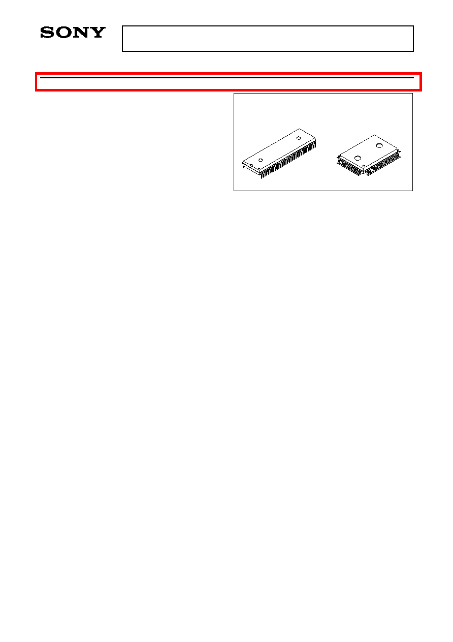
∑ Package
64-pin plastic SDIP/QFP
∑ Piggyback/evaluation chip
CXP85690 64-pin ceramic PSDIP (accommodates custom font)
Purchase of Sony's I
2
C components conveys a license under the Philips I
2
C Patent Rights to use these components
in an I
2
C system, provided that the system conform to the I
2
C Standard Specifications as defined by Philips.
Sony reserves the right to change products and specifications without prior notice. This information does not convey any license by
any implication or otherwise under any patents or other right. Application circuits shown, if any, are typical examples illustrating the
operation of the devices. Sony cannot assume responsibility for any problems arising out of the use of these circuits.
64 pin SDIP (PIastic)
64 pin QFP (PIastic)
Structure
Silicon gate CMOS IC
For the availability of this product, please contact the sales office.
≠ 2 ≠
CXP85632/85640
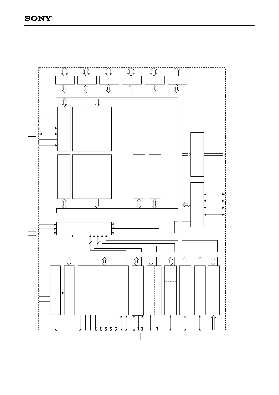
VIN
XLC
EXLC
R
G
B
I
YS
YM
HSYNC
VSYNC
SI
SO
SCK
EC
TO
RMC
HSC0
HSC1
AN0 to AN5
CVss
CV
DD
Cap
Rex
DATA SLICER
CC DECODER
ON SCREEN DISPLAY
SERIAL INTERFACE UNIT
8BIT TIMER/COUNTER 0
REMOCON
HSYNC COUNTER 0
HSYNC COUNTER 1
A/D CONVERTER 6CH
FIFO
3
2
INT2
INT1
INT0
SCL1
SCL0
SDA1
SDA0
I
2
C BUS
INTERFACE UNIT
8BIT PWM 4CH
WATCHDOG TIMER
PRESCALER/
TIME BASE TIMER
SPC700 CPU CORE
ROM
32K/40K BYTES
CLOCK GENERATOR/
SYSTEM CONTROL
RAM
1888 BYTES
Vss
V
DD
MP
RST
XTAL
EXTAL
PWM0 to PWM3
PA0 to PA7
8
PB0 to PB7
8
PC0 to PC7
8
PD0 to PD7
8
PE0 to PE2
3
PF0 to PF7
8
INTERRUPT CONTROLLER
PORT A
PORT B
PORT C
PORT D
PORT E
PORT F
8BIT TIMER 1
2
Block Diagram
≠ 3 ≠
CXP85632/85640
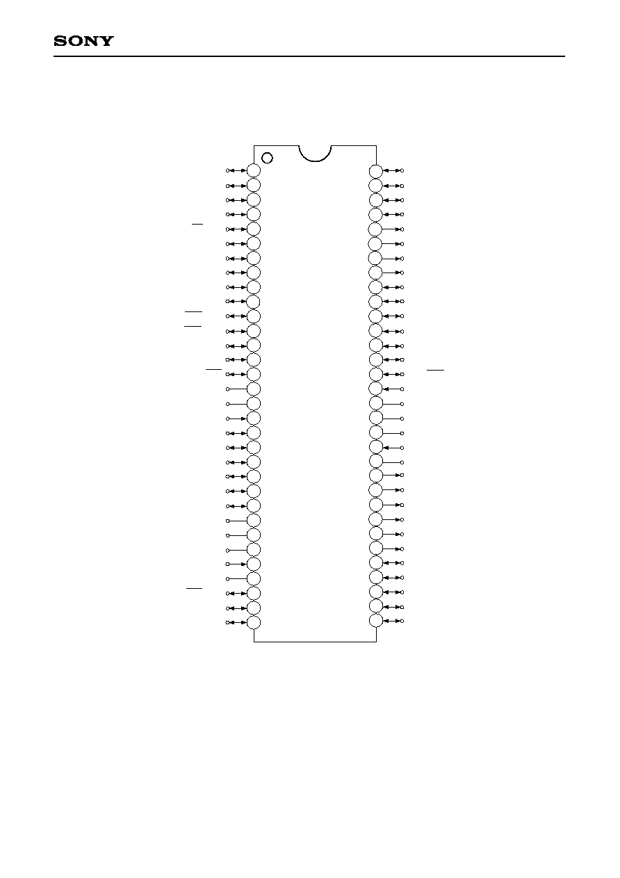
Pin Assignment (Top View) 64-pin SDIP
2
3
4
5
6
7
8
9
10
11
12
13
14
15
16
17
18
19
20
21
22
23
24
25
26
27
28
29
30
31
32
1
40
39
38
37
36
35
34
33
41
42
43
44
45
46
47
48
49
50
51
52
53
54
55
56
57
58
59
60
63
64
61
62
PC3
PC2
PC1
PC0
EC/PD7
RMC/PD6
HS1/PD5
HS0/PD4
SI/PD3
SO/PD2
SCK/PD1
INT2/PD0
HSYNC/PA7
VSYNC/PA6
RST
Vss
XTAL
EXTAL
PA5/AN5
PA4/AN4
PA3/AN3
PA2/AN2
PA1/AN1
PA0/AN0
CVss
Cap
Rex
VIN
CV
DD
INT1/PB7
PB6
PB5
PC4
PC5
PC6
PC7
PF0/PWM0
PF1/PWM1
PF2/PWM2
PF3/PWM3
PF4/SCL0
PF5/SCL1
PF6/SDA0
PF7/SDA1
PE0/TO
PE1
PE2/INT0
MP
Vss
V
DD
NC
EXLC
XLC
YM
YS
I
B
G
R
PB0
PB1
PB2
PB3
PB4
Note) 1. NC (Pin 46) must be connected to V
DD
.
2. Vss (Pins 16 and 48) must be connected to GND.
3. MP (Pin 49) must be connected to GND.
4. Cap (Pin 26) must be connected to CV
SS
via a capacitor.
5. Rex (Pin 27) must be connected to CV
DD
via a resistor of 33k
.
≠ 4 ≠
CXP85632/85640
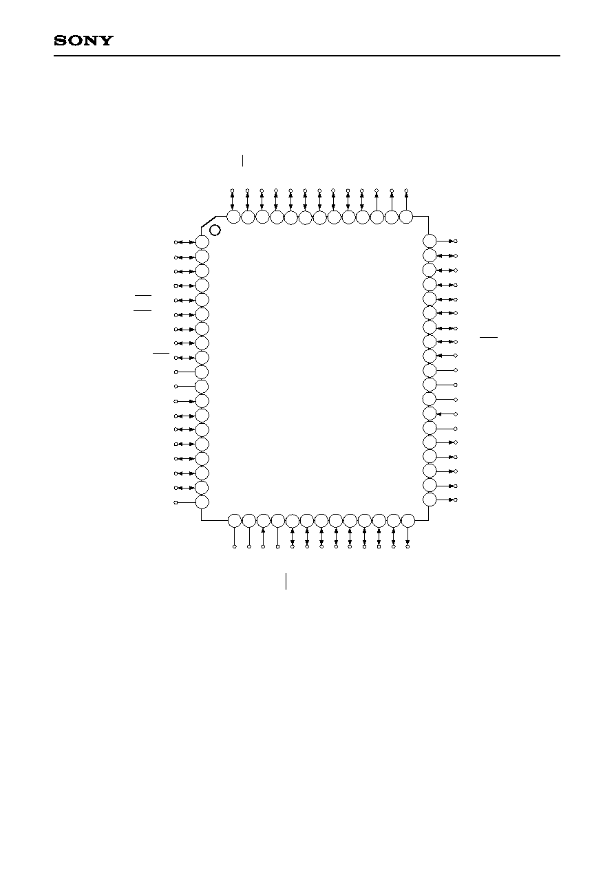
Pin Assignment (Top View) 64-pin QFP
HS1/PD5
HS0/PD4
SI/PD3
S0/PD2
SCK/PD1
INT2/PD0
HSYNC/PA7
VSYNC/PA6
RST
Vss
XTAL
EXTAL
PA5/AN5
PA4/AN4
PA3/AN3
PA2/AN2
PA1/AN1
PA0/AN0
CVss
2
3
4
5
6
7
8
9
10
11
12
13
14
15
16
17
18
19
1
PF3/PWM3
PF4/SCL0
PF5/SCL1
PF6/SDA0
PF7/SDA1
PE0/TO
PE1
PE2/INT0
MP
Vss
V
DD
NC
EXLC
XLC
YM
YS
I
B
G
40
39
38
37
36
35
34
33
41
42
43
44
45
46
47
48
49
50
51
PD6/RMC
PD7/EC
PC0
PC1
PC2
PC3
PC4
PC5
PC6
PC7
PF0/PWM0
PF1/PWM1
PF2/PWM2
52
53
54
55
56
57
58
59
60
63
64
61
62
Cap
Rex
VIN
CV
DD
INT1/PB7
PB6
PB5
PB4
PB3
PB2
PB1
PB0
R
20 21 22 23 24 25 26 27 28 29 30 31 32
Note) 1. NC (Pin 40) must be connected to V
DD
.
2. Vss (Pins 10 and 42) must be connected to GND.
3. MP (Pin 43) must be connected to GND.
4. Cap (Pin 20 ) must be connected to CV
SS
via a capacitor.
5. Rex (Pin 21) must be connected to CV
DD
via a resistor of 33k
.
≠ 5 ≠
CXP85632/85640
Pin Functions
Pin name
PA0/AN0
to
PA5/AN5
PA6/VSYNC
PA7/HSYNC
PB0 to PB6
PB7/INT1
PC0 to PC7
PD0/INT2
PD1/SCK
PD2/SO
PD3/SI
PD4/HS0
PD5/HS1
PD6/RMC
PD7/EC
PE0/TO
PE1
PE2/INT0
PF0/PWM0
to
PF3/PWM3
PF4/SCL0
PF5/SCL1
PF6/SDA0
PF7/SDA1
R, G, B, I, YS, YM
I/O/Analog input
I/O/Input
I/O/Input
I/O
I/O/Input
I/O
I/O/Input
I/O/I/O
I/O/Output
I/O/Input
I/O/Input
I/O/Input
I/O/Input
I/O/Input
I/O/Output
I/O
I/O/Input
Output/Output
Output/I/O
Output/I/O
Output
I/O
Functions
Analog inputs to A/D converter. (6 pins)
OSD display vertical sync signal input.
OSD display horizontal sync signal input.
Input for external interruption request. Active at
the falling edge.
Input for external interruption request. Active at
the falling edge.
Serial clock I/O.
Serial data output.
Serial data input.
HSYNC counter (CH0) input.
HSYNC counter (CH1) input.
Remote control receiver circuit input.
External event input for timer/counter.
Rectangular wave output for timer/counter.
Input for external interruption request.
Active at the falling edge.
8-bit PWM outputs.
(4 pins)
Transfer clock I/O for I
2
C bus interface. (2 pins)
Transfer data I/O for I
2
C bus interface. (2 pins)
(Port A)
8-bit I/O port. I/O
can be set in a unit
of single bits.
(8 pins)
(Port B)
8-bit I/O port. I/O can be set in a unit of single bits.
(8 pins)
(Port C)
8-bit I/O port. I/O can be set in a unit of single bits. (8 pins)
(Port D)
8-bit I/O port. I/O
can be set in a unit
of single bits.
Capable of driving
12mA sync current.
(8 pins)
(Port E)
3-bit I/O port. I/O
can be set in a unit
of single bits.
(3 pins)
(Port F)
8-bit output port
with large current
(12mA) N-ch open
drain output.
Lower 4 bits are
12V drive and upper
4 bits are 5V drive.
OSD display 6-bit outputs. (6 pins)
≠ 6 ≠
CXP85632/85640
Pin name
EXLC
XLC
VIN
Cap
Rex
CV
DD
CV
SS
EXTAL
XTAL
RST
MP
NC
V
DD
Vss
Input
Output
Input
--
--
Input
Output
I/O
Input
OSD display clock oscillation I/O.
Oscillator frequency is determined by external L and C.
Input of external composite video signal. Input a 2Vp-p signal via a
capacitor.
Capacitor connection for the data slicer. Connect a capacitor between
Cap and CV
SS
.
Resistor connection for the data slicer. Connect a 33k
resistor
between Rex and CV
DD
.
Positive power supply for data slicer.
GND for data slicer.
System clock oscillator crystal connection. When using an external
clock, input to EXTAL pin and leave XTAL pin open.
Low level active system reset. This pin acts as I/O pin and outputs low
level through incorporated power-on reset function when the power
turned on. (Mask option)
Test mode input. Must be connected to GND.
Not connected.
Under normal conditions, connect to V
DD
.
Positive power supply.
GND. Connect two V
SS
pins to GND.
I/O
Functions

≠ 7 ≠
CXP85632/85640
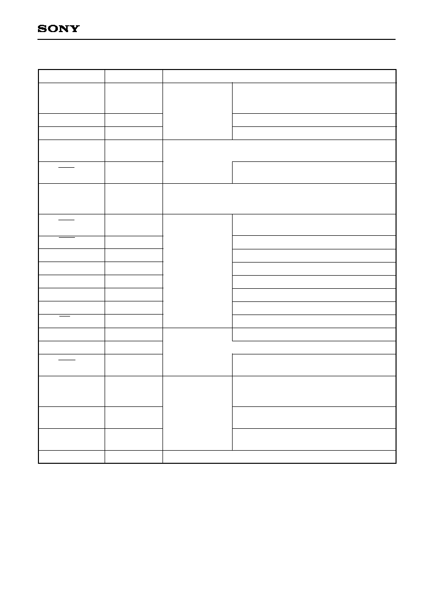
I/O Circuit Format for Pins
Data bus
Port A data
Port A direction
RD (Port A)
IP
VSYNC, HSYNC
Input polarity
Schmitt input
"0" when reset
Port A data
Port A direction
Data bus
RD (Port A)
Port A function selection
"0" when reset
IP
A/D converter
Input multiplexer
"0" when reset
Input
protection
circuit
Port B, C data
Port B, C direction
Data bus
RD (Port B, C)
INT1
IP
"0" when reset
Schmitt input
Port A
Port A
Port B
Port C
2 pins
6 pins
16 pins
Hi-Z
Hi-Z
Hi-Z
Pin
When reset
Circuit format
PA0/AN0
to
PA5/AN5
PB0 to PB6
PB7/INT1
PC0 to PC7
PA6/VSYNC
PA7/HSYNC
≠ 8 ≠
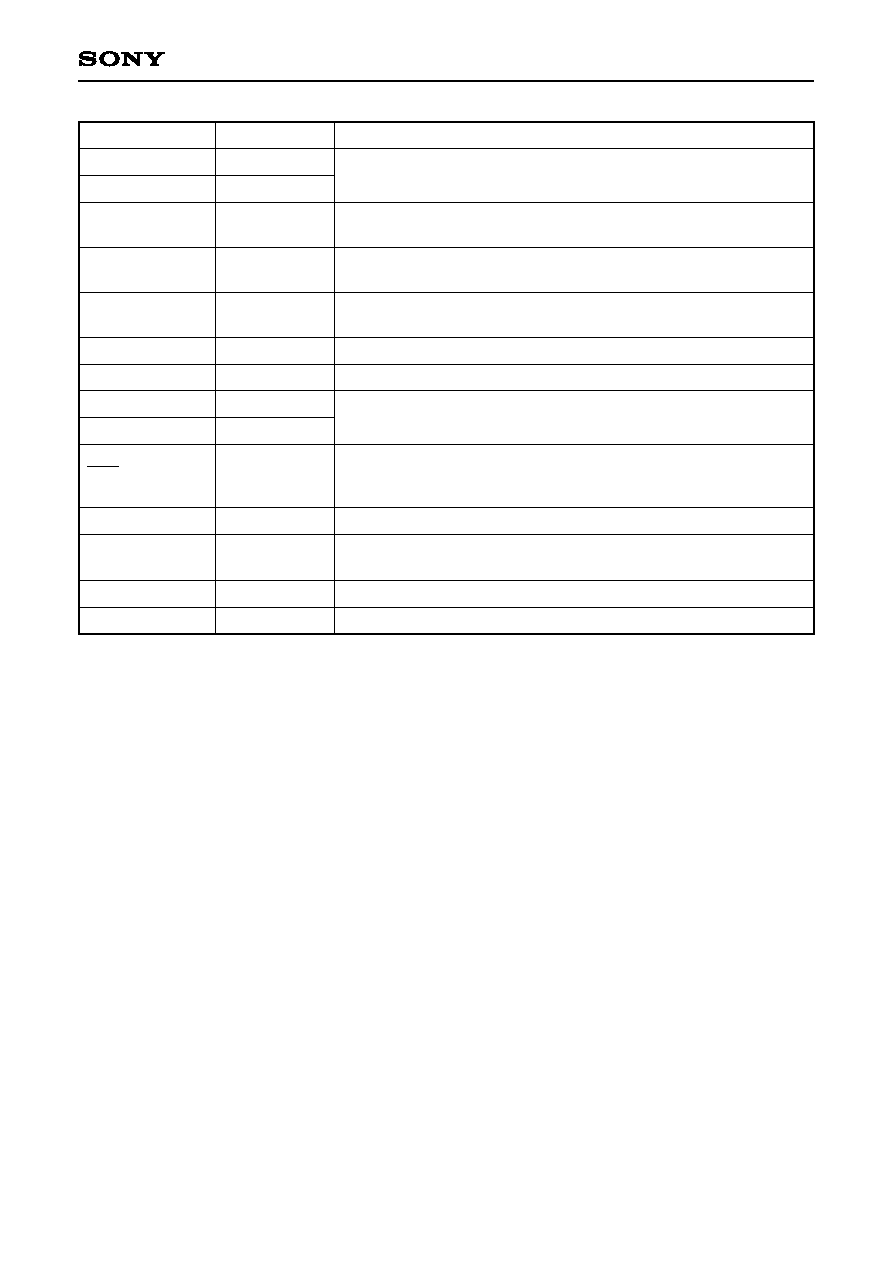
CXP85632/85640
Port D data
Port D direction
Data bus
RD (Port D)
INT2, SI, HS0, HS1, RMC, EC
Large current 12mA
IP
Schmitt input
"0" when reset
Port D data
Port D direction
Data bus
RD (Port D)
SCK only
Large current 12mA
SCK, SO
Serial output enable
Schmitt input
IP
"0" when reset
Port E function selection
TO
Port E direction
Port E data
Data bus
INT0
Schmitt input
only for PE2
RD (Port E)
"1" when reset
"1" when reset for PE0, 1
"1" when reset for PE0, 1
"0" when reset for PE2
IP
Port D
Port D
Port E
6 pins
2 pins
3 pins
Hi-Z
Hi-Z
PE0, PE1:
High
PE2: Hi-Z
Pin
When reset
Circuit format
PD1/SCK
PD2/SO
PE0/TO
PE1
PE2/INT0
PD0/INT2
PD3/SI
PD4/HS0
PD5/HS1
PD6/RMC
PD7/EC
≠ 9 ≠
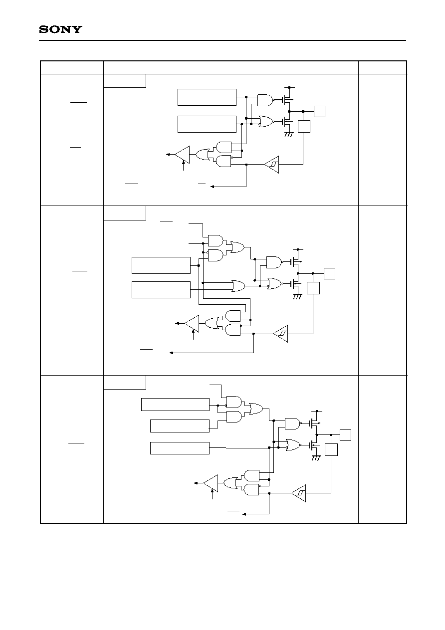
CXP85632/85640
SCL, SDA
Port F data
Large current 12mA
I
2
C output enable
IP
Schmitt input
SCL, SDA
(I
2
C circuit)
To internal I
2
C pins
(To SCL1 for SCL0)
BUS SW
"1" when reset
Port F selection
Port F data
PWM0 to PWM3
Large current 12mA
12V drive voltage
"0" when reset
"1" when reset
Port F
Port F
4 pins
4 pins
6 pins
2 pins
Pin
When reset
Circuit format
PF4/SCL0
PF5/SCL1
PF6/SDA0
PF7/SDA1
Hi-Z
Hi-Z
Hi-Z
Oscillation
halted
R
G
B
I
YS
YM
PF0/PWM0
to
PF3/PWM3
EXLC
XLC
R, G, B, I, YS, YM
Output becomes active
by data writing to output
polarity register.
Output polarity
"0" when reset
Oscillator control
EXLC
IP
OSD display clock
IP
XLC
≠ 10 ≠
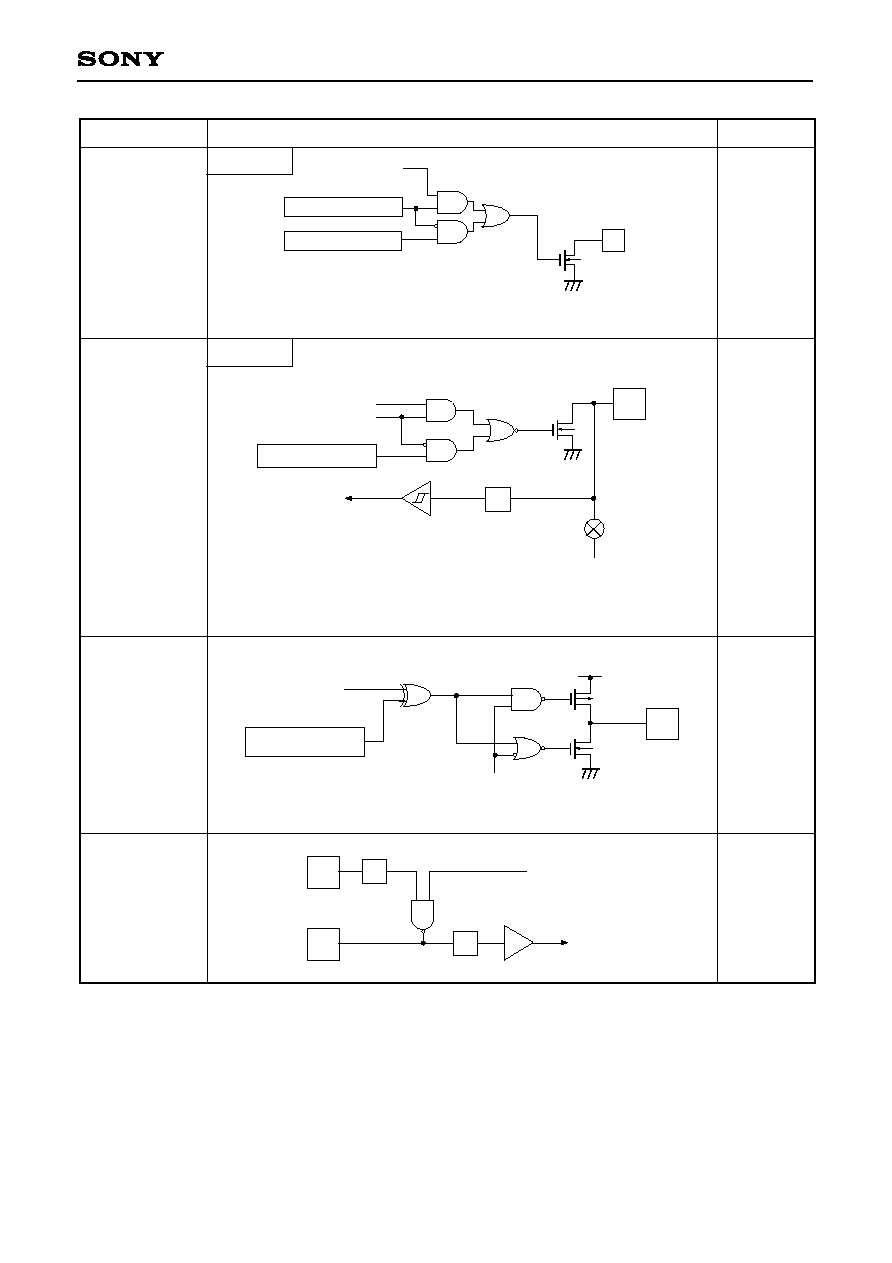
CXP85632/85640
2 pins
1 pin
Pin
When reset
Circuit format
RST
Oscillation
Low level
EXTAL
XTAL
IP
EXTAL
XTAL
∑ Diagram indicates equivalent
circuit during oscillation.
∑ Feedback resistor is disconnected
during STOP.
(This device does not enter in the
STOP mode.)
Schmitt input
Pull-up resistor
From power-on reset circuit
(Mask option)
Mask option
OP
≠ 11 ≠
CXP85632/85640
1
V
IN
and V
OUT
should not exceed V
DD
+ 0.3V.
2
The large current output port is Port D (PD) and Port F (PF).
Note) Usage exceeding absolute maximum ratings may permanently impair the LSI. Normal operation should
better take place under the recommended operating conditions. Exceeding those conditions may
adversely affect the reliability of the LSI.
Supply voltage
Input voltage
Output voltage
Medium voltage tolerance output voltage
High level output current
High level total output current
Low level output current
Low level total output current
Operating temperature
Storage temperature
Allowable power dissipation
V
DD
V
IN
V
OUT
V
OUTP
I
OH
I
OH
I
OL
I
OLC
I
OL
Topr
Tstg
P
D
≠0.3 to +7.0
≠0.3 to +7.0
1
≠0.3 to +7.0
1
≠0.3 to +15.0
≠5
≠50
15
20
100
≠20 to +75
≠55 to +150
1000
600
V
V
V
V
mA
mA
mA
mA
mA
∞C
∞C
mW
mW
PF0 to PF3 pins
Total of all output pins
Excludes large current output
port (value per pin)
Large current output port
(value per pin
2
)
Total of all output pins
SDIP
QFP
Item
Symbol
Ratings
Unit
Remarks
Absolute Maximum Ratings
(Vss = 0V reference)
5.5
5.5
5.5
5.5
V
DD
V
DD
V
DD
+ 0.3
0.3V
DD
0.2V
DD
0.4
+75
V
V
V
V
V
V
V
V
V
V
∞C
Item
Symbol
Min.
Max.
Unit
Remarks
4.5
3.5
2.5
4.5
0.7V
DD
0.8V
DD
V
DD
≠ 0.4
0
0
≠0.3
≠20
V
DD
1
This device does not enter in the STOP mode.
2
PA, PB, PC, PE0, PE1, SCL0, SCL1, SDA0, SDA1 pins.
3
INT2, SCK, SO, SI, HS0, HS1, RMC, EC, INT1, HSYNC, VSYNC, RST pins.
4
Specifies only during external clock input.
5
CV
DD
and V
DD
should be set to the same voltage.
Recommended Operating Conditions
(Vss = 0V reference)
Supply voltage
Data slicer supply
voltage
High level
input voltage
Low level
input voltage
Operating temperature
CV
DD
V
IH
V
IHS
V
IHEX
V
IL
V
ILS
V
ILEX
Topr
Guaranteed operation range for 1/2 or 1/4
frequency dividing mode
Guaranteed operation range for 1/16
frequency dividing or SLEEP mode
Guaranteed data hold range for STOP mode
1
5
2
3
EXTAL pin
4
2
3
EXTAL pin
4
≠ 12 ≠
CXP85632/85640
V
DD
= 4.5V, I
OH
= ≠0.5mA
V
DD
= 4.5V, I
OH
= ≠1.2mA
V
DD
= 4.5V, I
OL
= 1.8mA
V
DD
= 4.5V, I
OL
= 3.6mA
V
DD
= 4.5V, I
OL
= 3.0mA
V
DD
= 4.5V, I
OL
= 4.0mA
V
DD
= 5.5V, V
IH
= 5.5V
V
DD
= 5.5V, V
IL
= 0.4V
V
DD
= 4.5V, I
OL
= 12.0mA
High level
output voltage
Low level
output voltage
Input current
I/O leakage current
Open drain output
leak current
(N-ch Tr off case)
I
2
C bus switch
connection impedance
(Output Tr off case)
Supply current
Input capacitance
4.0
3.5
18
0.9
--
5.0
10
--
--
3
--
10.0
20
µA
mA
pF
50
10
120
30
mA
mA
µA
µA
0.4
0.6
1.5
0.4
0.6
40
≠40
≠400
±10
V
V
V
V
V
µA
µA
µA
µA
0.5
≠0.5
≠1.5
V
V
PA to PD, PE, R, G,
B, I, YS, YM
PA to PD, PE, R, G,
B, I, YS, YM,
PF0 to PF3, RST
1
PD, PF
PF4 to PF7
(SCL0, SCL1,
SDA0, SDA1)
EXTAL
RST
2
PA to PE, HSYNC,
VSYNC, R, G, B, I,
YS, YM, RST
2
PF0 to PF3
PF4 to PF7
SCL0: SCL1
SDA0: SDA1
V
DD
= 5.5V, V
IL
= 0.4V
V
DD
= 5.5V,
V
I
= 0, 5.5V
V
DD
= 5.5V, V
OH
= 12.0V
V
DD
= 5.5V, V
OH
= 5.5V
V
DD
= 4.5V
V
SCL0
= V
SCL1
= 2.25V
V
SDA0
= V
SDA1
= 2.25V
V
DD
3
CV
DD
STOP mode
4
V
DD
= 5.5V,
termination of 12MHz
oscillation
V
DD
= 5.5V
SLEEP mode
V
DD
= 5.5V,
12MHz crystal oscillation
(C
1
= C
2
= 15pF)
PA to PE, SCL, SDA,
EXLC, EXTAL, VIN,
RST
1MHz clock
0V for all pins excluding
measured pins
Item
Symbol
Pin
Condition
Min.
Typ.
Max.
Unit
V
OH
V
OL
I
IZ
I
LOH
R
BS
I
DD
I
DDSL
I
DDST
I
CVDD
C
IN
I
IHE
I
IHL
I
ILR
DC Characteristics
(Ta = ≠20 to +75∞C, Vss = 0V reference)
1
RST pin is specified only when the power-on reset circuit is selected with mask option.
2
In RST pin, the input current is specified when the pull-up resistor is selected; the leakage current when no
resistor is selected.
3
When all pins are open. Specifies only when the OSD oscillation stops.
4
This device does not enter in the STOP mode.
1/2 frequency dividing mode
V
DD
= 5.5V
12MHz crystal oscillation
(C
1
= C
2
= 15pF)
≠ 13 ≠
CXP85632/85640
AC Characteristics
(1) Clock timing
1
t
sys indicates three values according to the contents of the clock control register (CLC: 00FE
H
) upper
2 bits. (CPU clock selection)
t
sys (ns) = 2000/fc (Upper 2 bits = "00"), 4000/fc (Upper 2 bits = "01"), 16000/fc (Upper 2 bits = "11")
System clock frequency
System clock input
pulse width
System clock
rise and fall times
Event counter input
clock pulse widtth
Event counter input clock
rise and fall times
f
C
t
XL
,
t
XH
t
CR
,
t
CF
t
EH
,
t
EL
t
ER
,
t
EF
XTAL
EXTAL
EXTAL
EXTAL
EC
EC
MHz
ns
ns
ns
ms
Item
System
Pin
Condition
Min.
Max.
Unit
Fig. 1, Fig. 2
Fig. 1, Fig. 2
External clock drive
Fig 1, Fig 2
External clock drive
Fig. 3
Fig. 3
37.5
t
sys
1
+ 50
Typ.
12.0
200
20
(Ta = ≠20 to +75∞C, V
DD
= 4.5 to 5.5V, Vss = 0V reference)
Fig. 1. Clock timing
EXTAL
t
XH
t
XL
t
CF
t
CR
0.4V
V
DD
≠
0.4V
1/fc
Fig. 2. Clock applied condition
Crystal oscillator
Ceramic oscillator
EXTAL
XTAL
External clock
EXTAL
XTAL
OPEN
C
1
C
2
Fig. 3. Event count clock timing
EC
t
EH
t
EL
t
EF
t
ER
0.2V
DD
0.8V
DD

≠ 14 ≠
CXP85632/85640
(2) Serial transfer
(Ta = ≠20 to +75∞C, V
DD
= 4.5 to 5.5V, Vss = 0V reference)
Item
SCK cycle time
t
KCY
SCK
Input mode
Output mode
SCK input mode
SCK output mode
SCK input mode
SCK output mode
SCK input mode
SCK output mode
SCK input mode
SCK output mode
1000
8000/fc
400
4000/fc ≠ 50
100
200
200
100
200
100
ns
ns
ns
ns
ns
ns
ns
ns
ns
ns
SCK
SI
SI
SO
t
KH
t
KL
t
SIK
t
KSI
t
KSO
SCK
high and low level widths
SI input set-up time
(for SCK
)
SI input hold time
(for SCK
)
SCK
SO delay time
System
Pin
Condition
Min.
Max.
Unit
Note) The load condition for the SCK output mode, SO output delay time is 50pF + 1TTL.
Fig. 4. Serial transfer timing
0.2V
DD
0.8V
DD
t
KL
t
KH
SO
t
KCY
t
SIK
t
KSI
0.2V
DD
0.8V
DD
t
KSO
0.2V
DD
0.8V
DD
Output data
Input data
SI
SCK
≠ 15 ≠
CXP85632/85640
Resolution
Linearity error
Zero transition
voltage
Full-scale transition
voltage
Conversion time
Sampling time
Analog input voltage
V
ZT
1
V
FT
2
t
CONV
t
SAMP
V
IAN
AN0 to AN5
Ta = 25∞C
V
DD
= 5.0V
Vss = 0V
≠50
4910
160/f
ADC
3
12/f
ADC
3
0
10
4970
8
±1
70
5030
V
DD
Bits
LSB
mV
mV
µs
µs
V
Item
Symbol
Pin
Condition
Min.
Typ.
Max.
Unit
(3) A/D converter characteristics
(Ta = ≠20 to +75∞C, V
DD
= 4.5 to 5.5V, Vss = 0V reference)
Linearity error
V
ZT
V
FT
Analog input
FF
H
FE
H
01
H
00
H
Digital conversion value
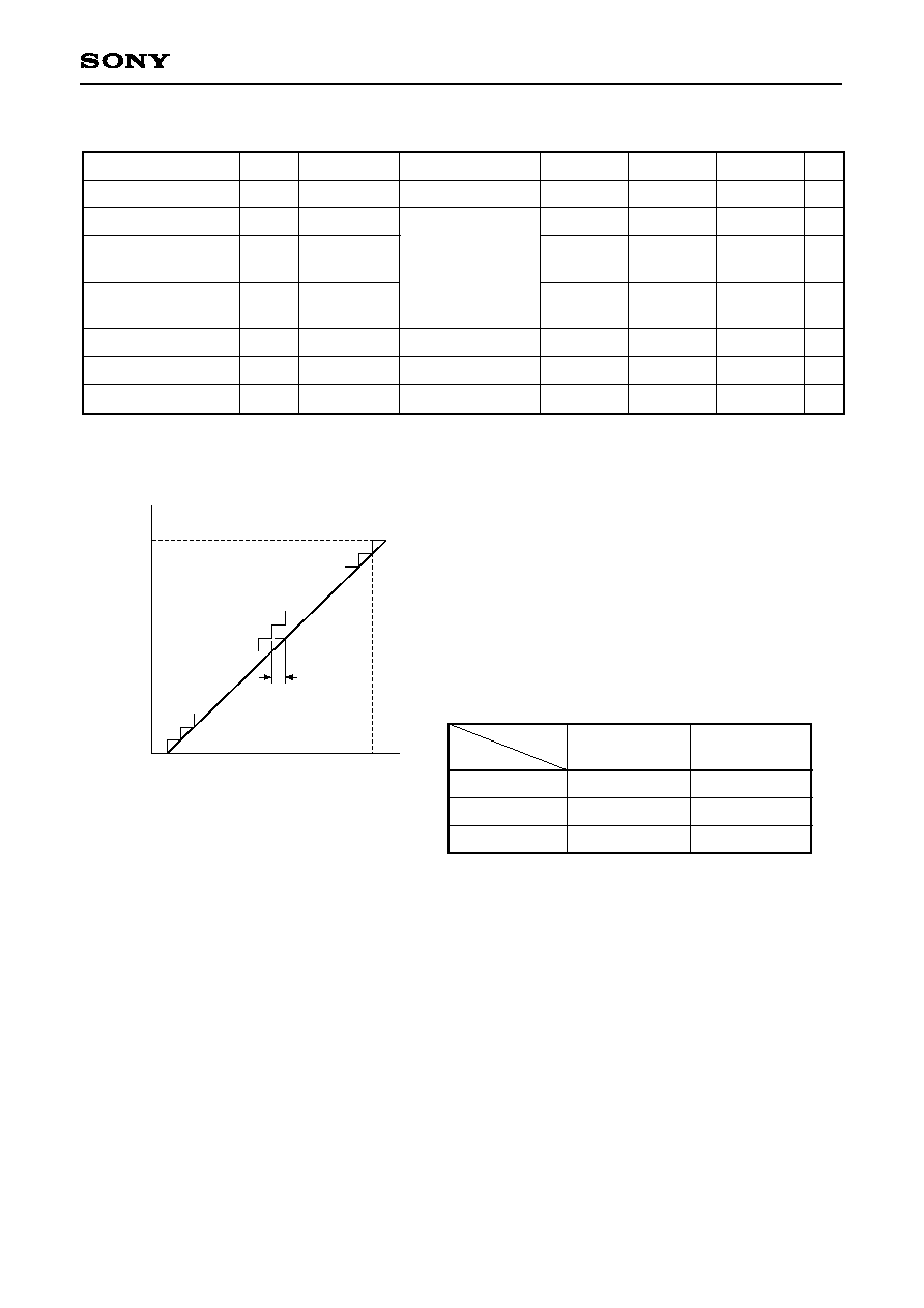
Fig. 5. Definitions for A/D converter terms
1
V
ZT
: Digital conversion values change between 00
H
01
H
.
2
V
FT
: Digital conversion values change between 0E
H
0F
H
.
3
f
ADC
indicates the below values due to the bit 6 (CKS) of
A/D control registor (ADC: 00F9
H
) and the bit 7 (PCK1) and
bit 6 (PCK0) of clock control registor (CLC: 00FE
H
)
00 (
= f
EX
/2)
01 (
= f
EX
/4)
11 (
= f
EX
/16)
f
ADC
= f
C
/2
f
ADC
= f
C
/4
f
ADC
= f
C
/16
f
ADC
= f
C
CKS
PCK1, 0
0 (
/2 selection)
1 (
selection)
f
ADC
= f
C
/2
f
ADC
= f
C
/8
≠ 16 ≠
CXP85632/85640
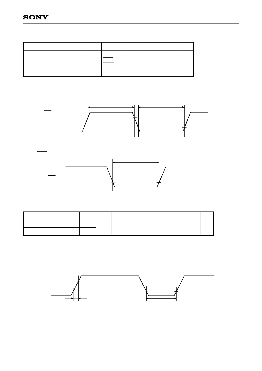
External interrupt
high and low level widths
Reset input low level width
INT0
INT1
INT2
RST
1
32/fc
µs
µs
Item
Symbol
Pin
Condition
Min.
Max.
Unit
t
IH
t
IL
t
RSL
Power supply rise time
Power supply cutt-off time
t
R
t
OFF
V
DD
Power-on reset
Repeated power-on reset
0.05
1
50
ms
ms
Item
Symbol
Pin
Condition
Min.
Max.
Unit
(4) Interrupt, reset input
(Ta = ≠20 to +75∞C, V
DD
= 4.5 to 5.5V, Vss = 0V reference)
(5) Power-on reset
1
(Ta = ≠20 to +75∞C, Vss = 0V reference)
0.2V
DD
0.8V
DD
t
IH
t
IL
INT0
INT1
INT2
(falling edge)
1
Specified only when power-on reset function is selected.
0.2V
0.2V
4.5V
V
DD
t
R
t
OFF
Take care when turning on power.
Fig. 6. Interrupt input timing
t
RSL
0.2V
DD
RST
Fig. 7. RST input timing
Fig. 8. Power-on reset
≠ 17 ≠
CXP85632/85640
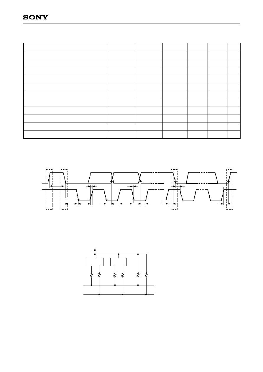
(6) I2C bus timing
(Ta = ≠20 to +75∞C, V
DD
= 4.5 to 5.5V, Vss = 0V reference)
Item
SCL clock frequency
Bus-free time before starting transfer
Hold time for starting transfer
Clock low level width
Clock high level width
Set-up time for repeated transfers
Data hold time
Data set-up time
SDA, SCL rise time
SDA, SCL fall time
Set-up time for transfer completion
f
SLC
t
BUF
t
HD; STA
t
LOW
t
HIGH
t
SU; STA
t
HD; DAT
t
SU; DAT
t
R
t
F
t
SU; STO
SCL
SDA, SCL
SDA, SCL
SCL
SCL
SDA, SCL
SDA, SCL
SDA, SCL
SDA, SCL
SDA, SCL
SDA, SCL
0
4.7
4.0
4.7
4.0
4.7
0
1
250
4.7
100
1
300
kHz
µs
µs
µs
µs
µs
µs
ns
µs
ns
µs
Symbol
Pin
Condition
Min.
Max.
Unit
1
For data hold time, the SCL rise time is not taken into account so that 300ns must be exceeded.
Fig. 9. I
2
C bus transfer data timing
P
St
t
SU; STO
t
SU; STA
t
HD; STA
t
SU; DAT
t
HIGH
t
HD; DAT
t
F
t
R
t
LOW
t
HD; STA
S
P
t
BUF
SDA
SCL
Fig. 10. I
2
C device recommended circuit
I
2
C
device
I
2
C
device
R
S
R
S
R
S
R
S
R
P
R
P
SDA0
(or SDA1)
SCL0
(or SCL1)
∑ A pull-up resistor must be connected to SDA0 (or SDA1), and SCL0 (or SCL1).
∑ The SDA0 (or SDA1) and SCL0 (or SCL1) series resistance (Rs = 300
or less) can be used to reduce spike
noise caused by CRT flashover.
≠ 18 ≠
CXP85632/85640
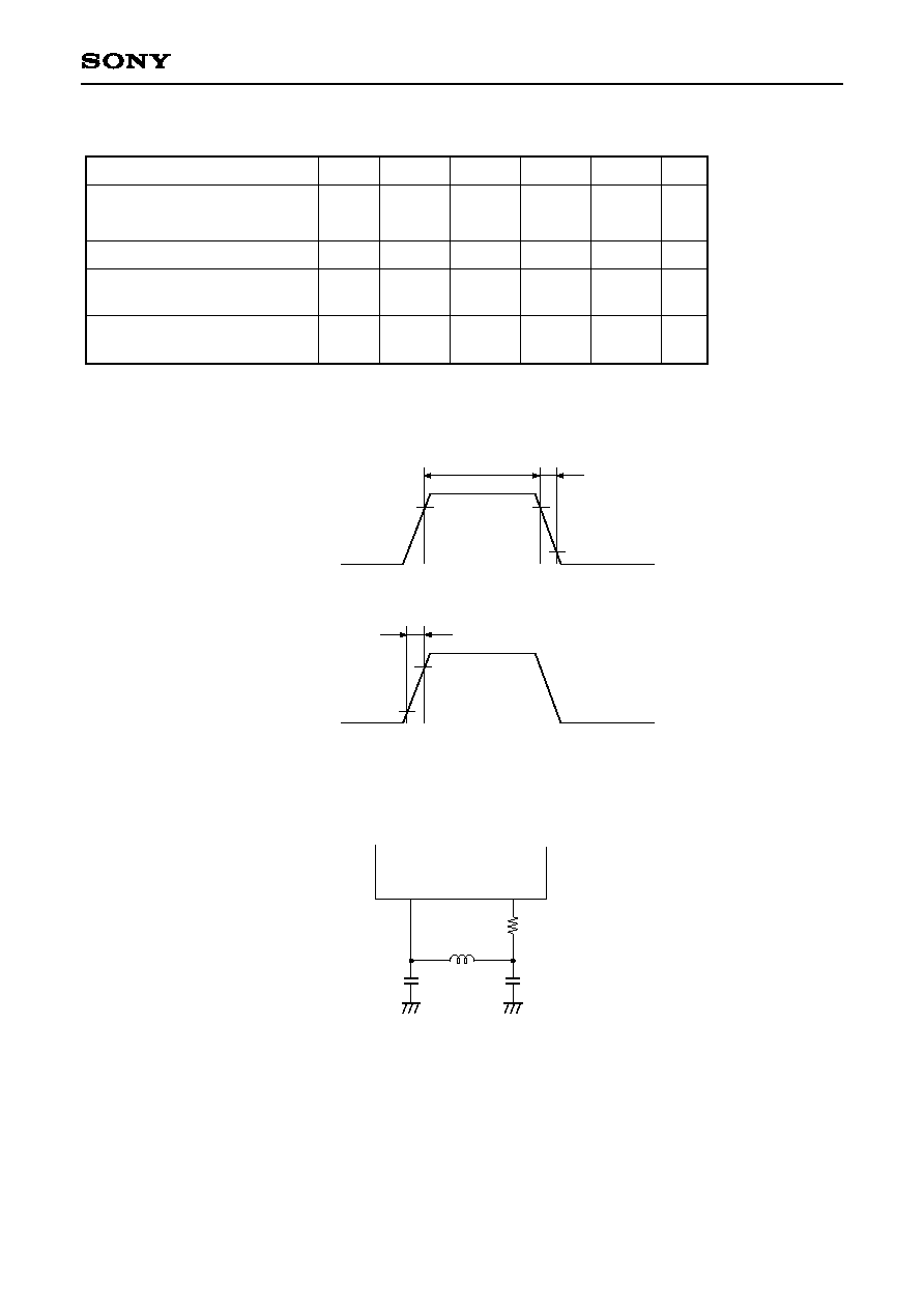
(7) OSD (On Screen Display) timing
(Ta = ≠20 to +75∞C, V
DD
= 4.5 to 5.5V, Vss = 0V reference)
Item
OSD clock frequency
HSYNC pulse width
HSYNC after-write
rise and fall times
VSYNC before-write
rise and fall times
f
OSC
t
HWD
t
HCG
t
VCG
EXLC
XLC
HSYNC
HSYNC
VSYNC
Fig. 12
Fig. 11
Fig. 11
Fig. 11
4
1.2
16.5
200
1.0
MHz
µs
ns
µs
Symbol
Pin
Condiiton
Unit
Min.
Max.
Fig. 11. OSD timing
0.8V
DD
0.2V
DD
t
HCG
t
HWD
HSYNC
For OPOL register (01FD
H
)
bit 7 at "0"
0.8V
DD
0.2V
DD
t
VCG
VSYNC
For OPOL register (01FD
H
)
bit 6 at "0"
Fig. 12. LC oscillator circuit connection
L
C
2
C
1
EXLC
XLC
R
1
1
The XLC series resistor can reduce the occurrence of undersired radiation.
≠ 19 ≠
CXP85632/85640
(8) Data slicer external circuit
(Ta = ≠20 to +75∞C, V
DD
= 4.5 to 5.5V, Vss = 0V reference)
Item
VIN pin coupling capacitor
Cap pin capacitor
Rex pin pull-up resistor
Composite video signal input
C
VIN
Ccap
Rrex
Video In
VIN
Cap
Rex
VIN
0.47
4700
33
2.0
µF
pF
k
Vp-p
Symbol
Pin
Min.
Unit
Typ.
Max.
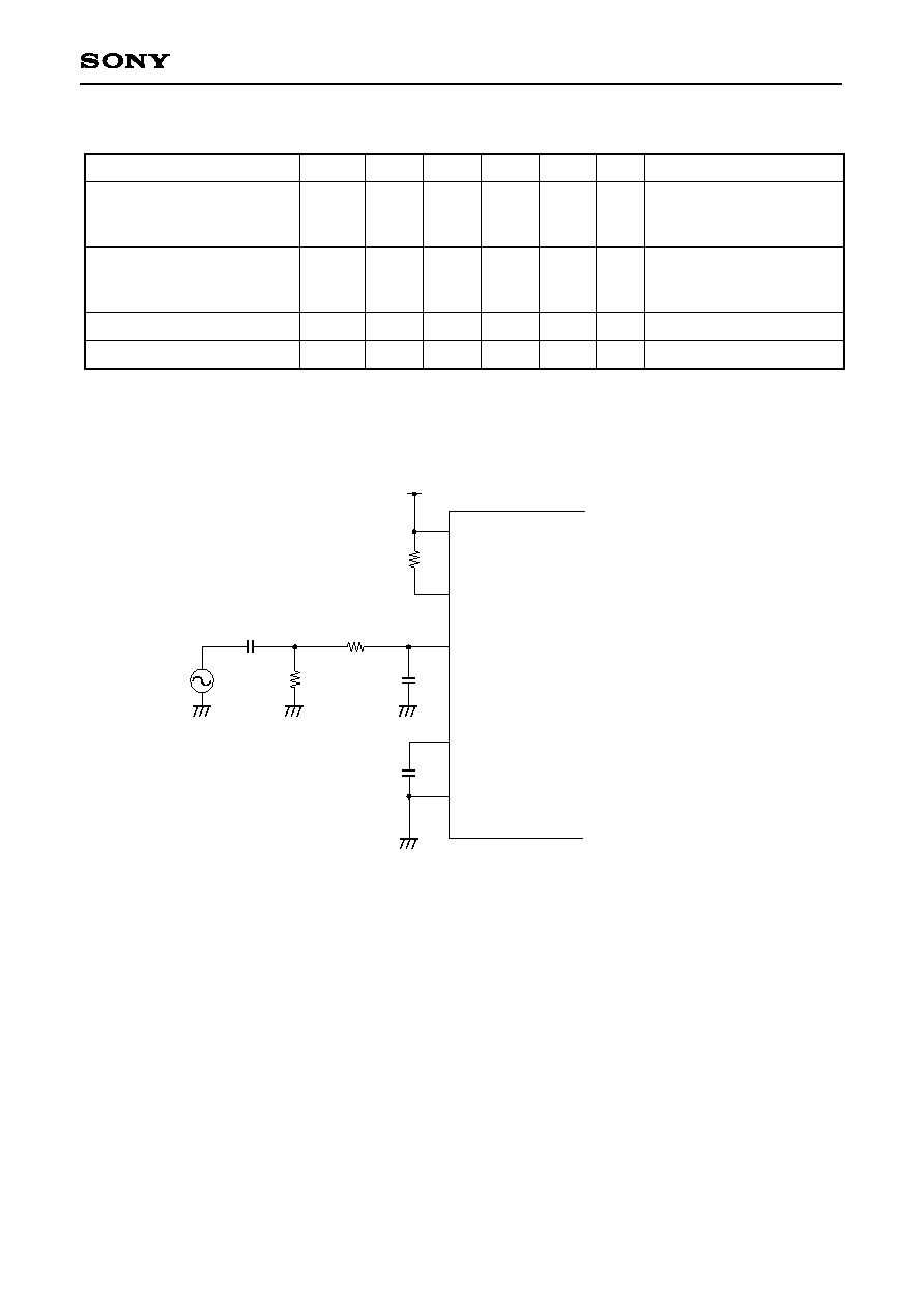
Fig. 13. Data slicer external recommeded circuit
B or more of temperature
characteristics is
recommended.
B or more of temperature
characteristics is
recommended.
Remarks
CV
DD
Rex
V
IN
Cap
CVss
Ccap
C
1
R
2
Video In
C
VIN
R
1
Rrex
5.0V
[Recommended Constant]
R
1
= 100
(error: 5%; allowable power dissipation: 1/8 W or more)
R
2
= 1M
(error: 5%; allowable power dissipation: 1/8 W or more)
C
1
= 820pF (ceramic), B or more of temperature characteristics is recommended.
≠ 20 ≠
CXP85632/85640
Supplement
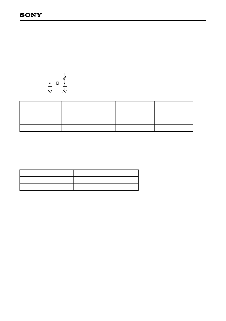
Fig. 14. SPC700 Series recommended oscillation circuit
C
2
C
1
EXTAL
XTAL
Rd
EXTAL
XTAL
Rd
(i)
Manufacturer
KINSEKI LTD.
Model
fc (MHz)
5
5
0
1
C
1
(pF)
C
2
(pF)
Rd (
)
Circuit
example
(i)
15
15
0
1
(i)
1
The XTAL series resistor can reduce the effect of electrostatic discharge noise.
Item
Inclusion
Reset pin pull-up resistor
Power-on reset circuit
Non-existent
Non-existent
Existent
Existent
Mask Option Table
RIVER ELETEC
CO., LTD.
12.0
12.0
HC-49/U03
HC-19/U (-S)
≠ 21 ≠
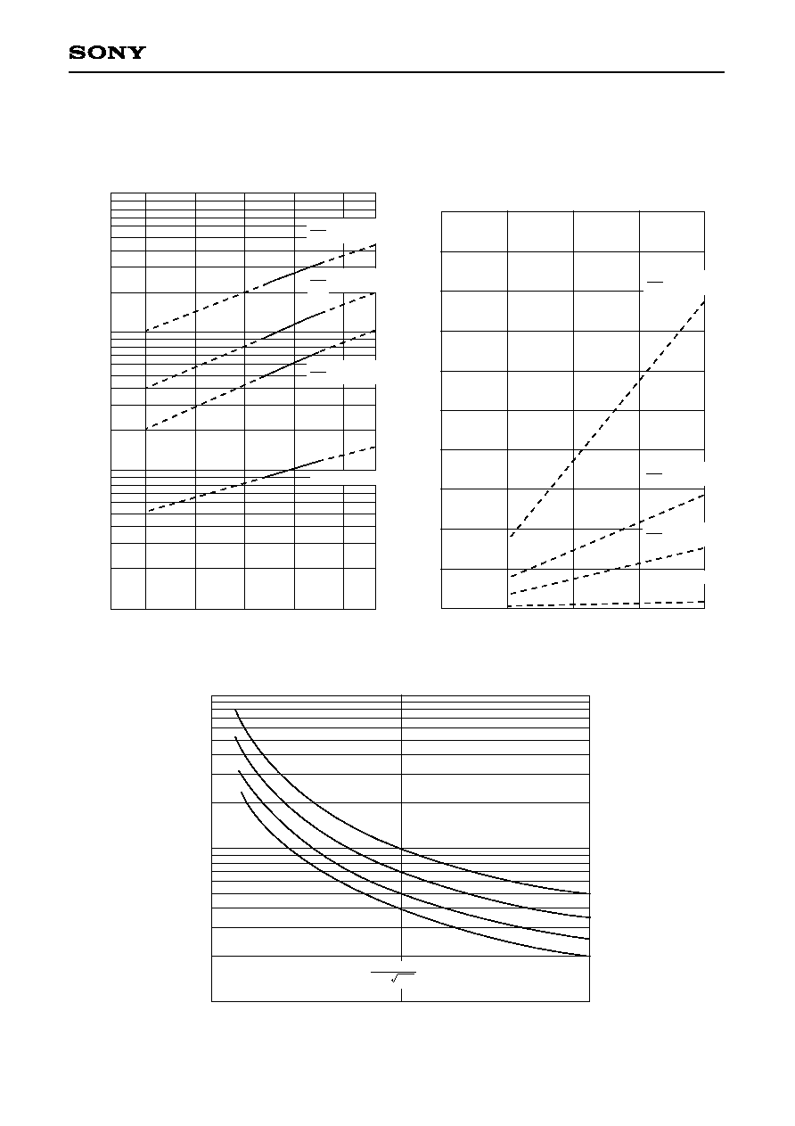
CXP85632/85640
Fig. 15. Characteristics curves
I
DD ≠
Supply current [mA]
I
DD
vs. V
DD
(fc = 12MHz, Ta = 25∞C, Typical)
V
DD ≠
Supply voltage [V]
2
3
4
5
6
0.1
100
I
DD
vs. fc
frequency
dividing mode
1
16
SLEEP mode
frequency
dividing mode
1
4
frequency
dividing mode
1
2
10
1
SLEEP mode
frequency
dividing mode
1
16
frequency
dividing mode
1
4
frequency
dividing mode
1
2
I
DD ≠
Supply current [mA]
50
45
40
35
30
25
20
15
10
5
0
fc
≠
System clock [MHz]
16
12
8
4
Parameter curve for OSD oscillation L vs. C
(theoretically calculated value)
10MHz
12MHz
14MHz
100
10
0
L
≠
Inductance [µ
H]
50
100
C
1
, C
2 ≠
Capacitance [pF]
f
OSC
= C = C
1 //
C
2
(V
DD
= 5V, Ta = 25∞C, Typical)
16MHz
1
2
LC
≠ 22 ≠
CXP85632/85640
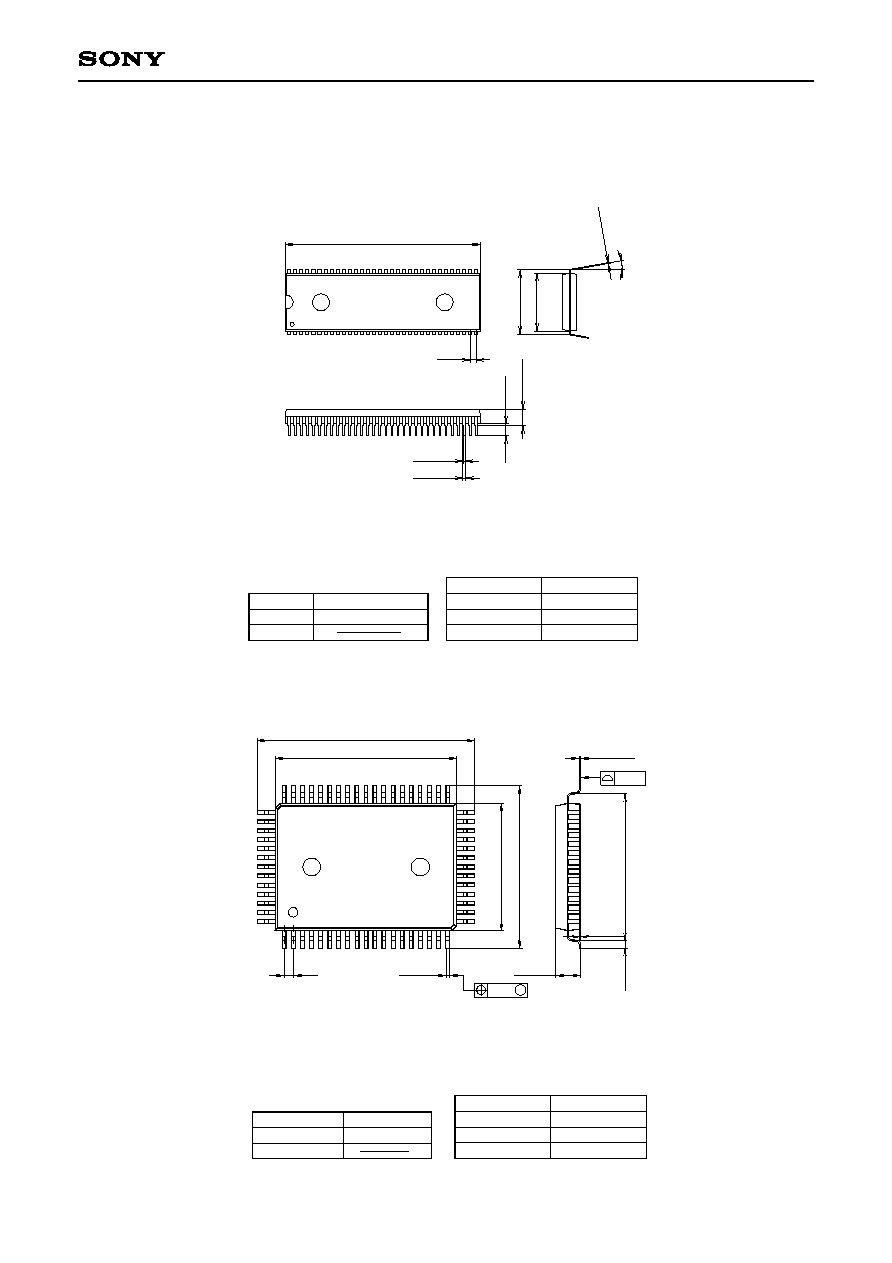
Package Outline
Unit: mm
PACKAGE STRUCTURE
MOLDING COMPOUND
LEAD TREATMENT
LEAD MATERIAL
PACKAGE WEIGHT
SONY CODE
EIAJ CODE
JEDEC CODE
SDIP-64P-01
42 ALLOY
SOLDER PLATING
EPOXY / PHENOL RESIN
64PIN SDIP (PLASTIC) 750mil
SDIP064-P-0750-A
57.6 ≠ 0.1
+ 0.4
64
33
1
32
1.778
19.05
17.1 ≠ 0.1
+ 0.3
0∞ to 15∞
0.25 ≠ 0.05
+ 0.1
0.5 MIN
4.75 ≠ 0.1
+ 0.4
3 MIN
0.5 ± 0.1
0.9 ± 0.15
8.6g
SONY CODE
EIAJ CODE
JEDEC CODE
23.9 ± 0.4
20.0 ≠ 0.1
1.0
0.4 ≠ 0.1
+ 0.15
14.
0
≠
0.
1
1
19
20
32
33
51
52
64
0.15 ≠ 0.05
+ 0.1
2.75 ≠ 0.15
16.
3
0.1 ≠ 0.05
+ 0.2
0.
8 ±
0.
2
M
± 0.12
0.15
+ 0.4
17.9 ±
0.4
+
0.
4
+ 0.35
64PIN QFP(PLASTIC)
QFP≠64P≠L01
QFP064≠P≠1420
PACKAGE MATERIAL
LEAD TREATMENT
LEAD MATERIAL
PACKAGE WEIGHT
EPOXY RESIN
SOLDER/PALLADIUM
COPPER /42 ALLOY
PACKAGE STRUCTURE
PLATING
1.5g