≠ 1 ≠
CXP856P40
E96740-PS
CMOS 8-bit Single Chip Microcomputer
Description
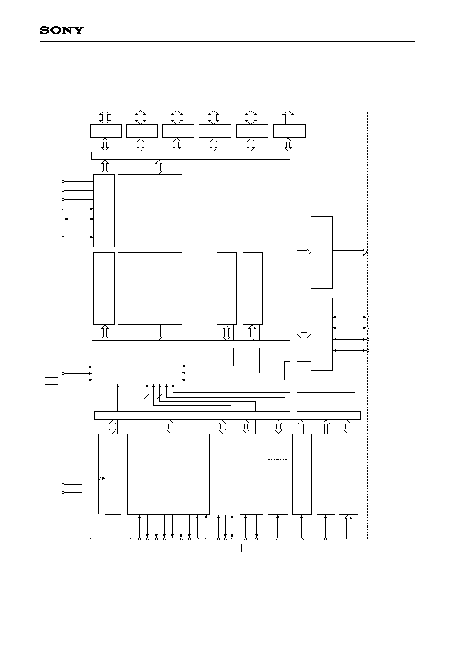
The CXP856P40 is a CMOS 8-bit microcomputer
which consists of A/D converter, serial interface,
timer/counter, time-base timer, closed caption decoder,
data slicer, on-screen display function, I
2
C bus
interface, PWM output, remote control reception
circuit, HSYNC counter and watchdog timer as well
as basic configuration like 8-bit CPU, PROM, RAM
and I/O port.
Also this IC provides a power-on reset function
and SLEEP function that enables to lower power
consumption.
CXP856P40 is the PROM-incorporated version of
the CXP85640 with built-in mask ROM. This
provides the additional feature of being able to
write directly into the program (also into the OSD
character ROM or caption character ROM
possible). Thus, it is most suitable for evaluation
use during system development and for small-
quantity production.
Features
∑ A wide instruction set (213 instructions) to cover various types of data
-- 16-bit operation/multiplication and division/Boolean bit operation instructions
∑ Minimum instruction cycle
333ns at 12MHz operation
∑ Incorporated PROM
40K bytes (Programming)
3K bytes (OSD)
3K bytes (Caption)
∑Incorporated RAM
1888 bytes (Excludes the closed caption decoder and on-screen display VRAM)
∑ Peripheral functions
-- A/D converter
8 bits, 6 channels, successive approximation method
(Conversion time of 26.7µs/12MHz)
-- Serial interface
8-bit clock sync type, 1 channel
-- Timer
8-bit timer, 8-bit timer/counter, 19-bit time-base timer
-- Closed caption decoder
Incorporated decode slicer,
conforming to FCC, 8
◊
13 dots, 192 character types, 15 character colors,
4 lines
◊
34 characters, italic, underline, vertical scrolling,
15 frame background colors/half blanking
-- On-screen display (OSD) function
12
◊
16 dots, 128 character types, 15 character colors, 4 lines
◊
24 characters,
edging (half dot) vertical scrolling for every line
8 frame background colors/half blanking, jitter elimination circuit
-- I
2
C bus interface
-- PWM output
8 bits, 4 channels
-- Remote control receiver circuit
8-bit pulse measurement counter, 6-stage FIFO
-- HSYNC counter
2 channels
-- Watchdog timer
∑ Interruption
15 factors, 15 vectors, multi-interruption possible
∑ Standby mode
Sleep
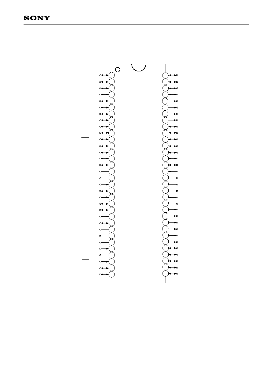
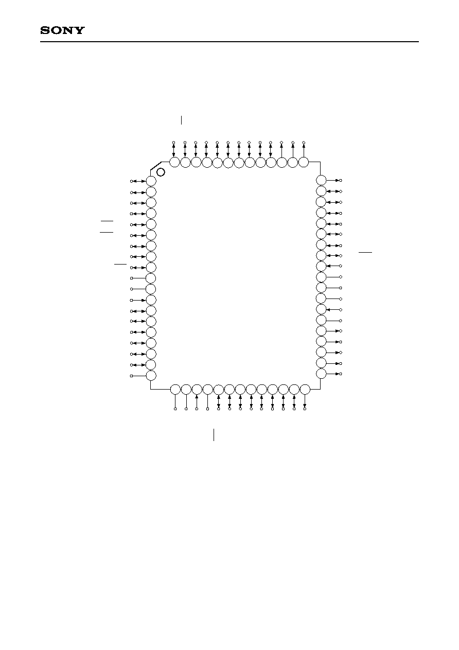
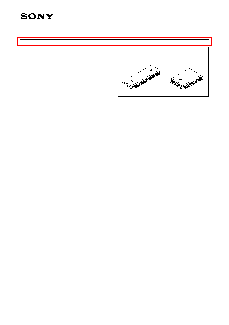
∑ Package
64-pin plastic SDIP/QFP
Purchase of Sony's I
2
C components conveys a license under the Philips I
2
C Patent Rights to use these components
in an I
2
C system, provided that the system conform to the I
2
C Standard Specifications as defined by Philips.
Sony reserves the right to change products and specifications without prior notice. This information does not convey any license by
any implication or otherwise under any patents or other right. Application circuits shown, if any, are typical examples illustrating the
operation of the devices. Sony cannot assume responsibility for any problems arising out of the use of these circuits.
64 pin SDIP (PIastic)
64 pin QFP (PIastic)
Structure
Silicon gate CMOS IC
For the availability of this product, please contact the sales office.
≠ 5 ≠
CXP856P40
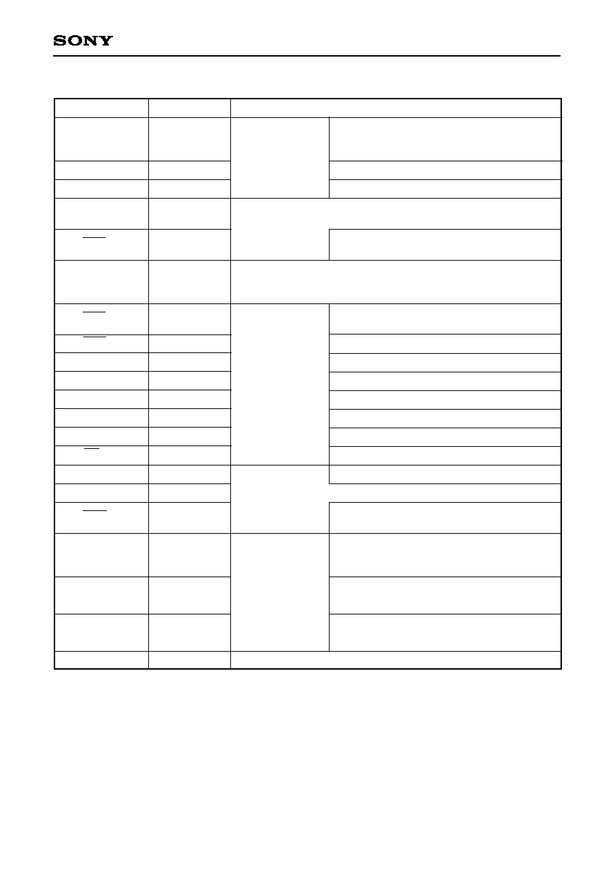
Pin Description
Symbol
PA0/AN0
to
PA5/AN5
PA6/VSYNC
PA7/HSYNC
PB0 to PB6
PB7/INT1
PC0 to PC7
PD0/INT2
PD1/SCK
PD2/SO
PD3/SI
PD4/HS0
PD5/HS1
PD6/RMC
PD7/EC
PE0/TO
PE1
PE2/INT0
PF0/PWM0
to
PF3/PWM3
PF4/SCL0
PF5/SCL1
PF6/SDA0
PF7/SDA1
R, G, B, I, YS, YM
I/O/Analog input
I/O/Input
I/O/Input
I/O
I/O/Input
I/O
I/O/Input
I/O/I/O
I/O/Output
I/O/Input
I/O/Input
I/O/Input
I/O/Input
I/O/Input
I/O/Output
I/O
I/O/Input
Output/Output
Output/I/O
Output/I/O
Output
I/O
Description
Analog inputs to A/D converter. (6 pins)
OSD display vertical sync signal input.
OSD display horizontal sync signal input.
External interruption request input.
Active at the falling edge.
External interruption request input.
Active at the falling edge.
Serial clock I/O.
Serial data output.
Serial data input.
HSYNC counter (CH0) input.
HSYNC counter (CH1) input.
Remote control reception circuit input.
External event input for timer/counter.
Rectangular wave output for timer/counter.
Input for external interruption request.
Active at the falling edge.
8-bit PWM outputs.
(4 pins)
Transfer clock I/O for I
2
C bus interface. (2 pins)
Transfer data I/O for I
2
C bus interface. (2 pins)
(Port A)
8-bit I/O port. I/O
can be set in a unit
of single bits.
(8 pins)
(Port B)
8-bit I/O port. I/O can be set in a unit of single bits.
(8 pins)
(Port C)
8-bit I/O port. I/O can be set in a unit of single bits. (8 pins)
(Port D)
8-bit I/O port. I/O
can be set in a unit
of single bits.
Can drive 12mA
sync current.
(8 pins)
(Port E)
3-bit I/O port. I/O
can be set in a unit
of single bits.
(3 pins)
(Port F)
8-bit output port
with large current
(12mA) N-ch open
drain output.
Lower 4 bits are
12V drive and upper
4 bits are 5V drive.
(8 pins)
6-bit OSD display outputs. (6 pins)