/home/web/htmldatasheet/RUSSIAN/html/sony/169193
CMOS 8-bit Single Chip Microcomputer
Description
The CXP86608/86612/86616 are the CMOS 8-bit
single chip microcomputer integrating on a single
chip an A/D converter, serial interface, timer/counter,
time-base timer, I
2
C bus interface, PWM output, remote
control reception circuit, watchdog timer, 32kHz timer/
counter besides the basic configurations of 8-bit CPU,
ROM, RAM, I/O ports.
The CXP86608/86612/86616 also provide a sleep
function that enables to lower the power consumption.
Features
· A wide instruction set (213 instructions) which covers
various types of data
-- 16-bit operation/multiplication and division/
Boolean bit operation instructions
· Minimum instruction
250ns at 16MHz operation
cycle
122µs at 32kHz operation
· Incorporated ROM
8K bytes (CXP86608)
12K bytes (CXP86612)
16K bytes (CXP86616)
· Incorporated RAM
352 bytes
· Peripheral functions
-- A/D converter
8 bits, 6 channels, successive approximation method
(Conversion time of 3.25µs at 16MHz)
-- Serial interface
8-bit clock sync type, 1 channel
-- Timer
8-bit timer
8-bit timer/counter
19-bit time-base timer
32kHz timer/counter
-- I
2
C bus interface
-- PWM output
8 bits, 4 channels
-- Remote control reception circuit
8-bit pulse measurement counter, 6-stage FIFO
-- Watchdog timer
· Interruption
11 factors, 11 vectors, multi-interruption possible
· Standby mode
Sleep
· Package
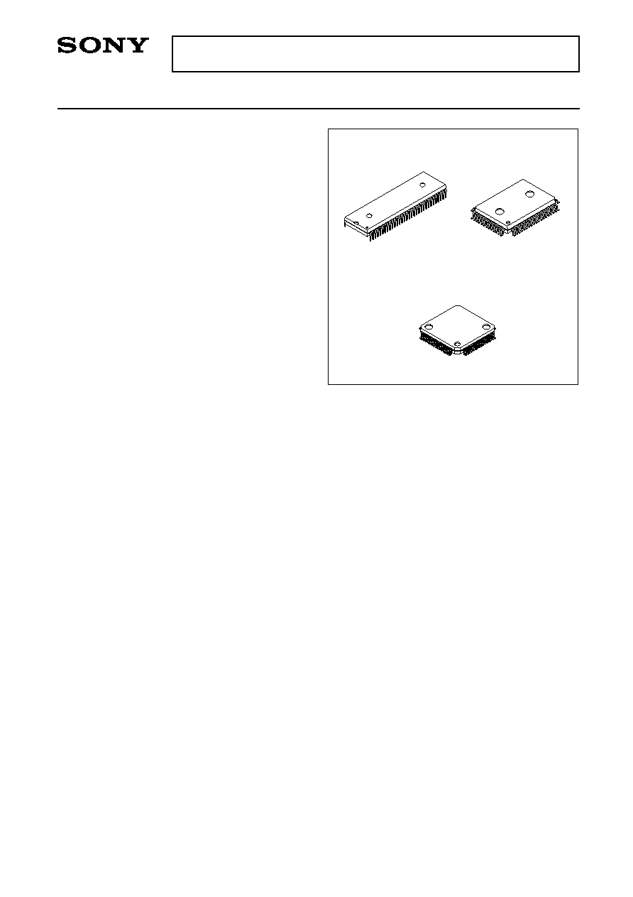
64-pin plastic SDIP/QFP/LQFP
· Piggyback/evaluator
CXP86400 64-pin ceramic PQFP
CXP86490 64-pin ceramic PSDIP
Perchase of Sony's I
2
C components conveys a licence under the Philips I
2
C Patent Rights to use these components
in an I
2
C system, provided that the system conforms to the I
2
C Standard Specifications as defined by Philips.
1
E97750C24-PS
Sony reserves the right to change products and specifications without prior notice. This information does not convey any license by
any implication or otherwise under any patents or other right. Application circuits shown, if any, are typical examples illustrating the
operation of the devices. Sony cannot assume responsibility for any problems arising out of the use of these circuits.
CXP86608/86612/86616
64 pin SDIP (Plastic)
64 pin QFP (Plastic)
Structure
Silicon gate CMOS IC
64 pin LQFP (Plastic)
2
CXP86608/86612/86616
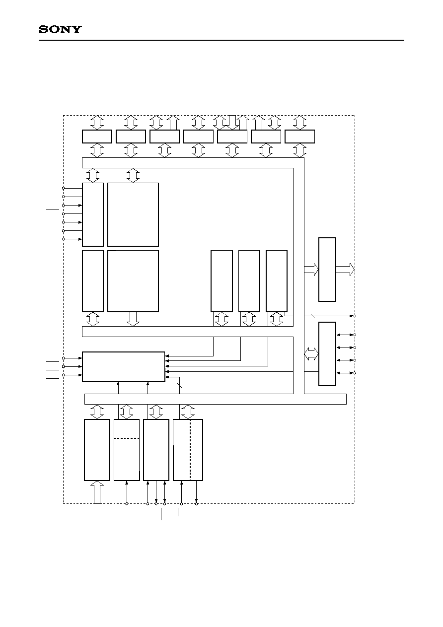
A/D CONVERTER
6CH
FIFO
REMOCON
SERIAL INTERFACE
UNIT
8-BIT TIMER 1
8-BIT TIMER/
COUNTER 0
I
2
C BUS
INTERFACE UNIT
8-BIT PWM
PRESCALER/
TIME BASE TIMER
WATCHDOG TIMER
32kHz
TIMER/COUNTER
ROM
8K/12K/16K
BYTES
RAM
352
BYTES
SPC700 CPU CORE
CLOCK GENERATOR
/SYSTEM CONTROL
INTERRUPT CONTROLLER
PORT A
PORT B
PORT C
PORT D
PORT E
PORT F
PORT G
PG3 to PG7
5
PF0 to PF3
4
PE4 to PE6
3
PE2 to PE3
2
PE0 to PE1
2
PD0 to PD7
8
PC6 to PC7
2
PC0 to PC5
6
PB0 to PB7
8
PA0 to PA7
8
PWM0 to PWM3
ADJ
SCL1
SCL0
SDA1
SDA0
TO
EC
SCK
SO
SI
RMC
AN0 to AN5
6
2
2
INT0
INT1
INT2
TEX
TX
EXTAL
XTAL
RST
V
DD
V
SS
4
PF4 to PF7
4
Block Diagram
3
CXP86608/86612/86616
40
39
38
37
36
35
34
33
41
42
43
44
45
46
47
48
49
50
51
52
53
54
55
56
57
58
59
60
63
64
61
62
31
32
2
3
4
5
6
7
8
9
10
11
12
13
14
15
16
17
18
19
20
21
22
23
24
25
26
27
28
29
30
1
V
SS
V
DD
NC
NC
NC
PE4
PE5
PE6
NC
NC
NC
PB0
PB1
PB2
PG3
PG4
PC4
PC5
PC6
PC7
PF0/PWM0
PF1/PWM1
PF2/PWM2
PF3/PWM3
PF4/SCL0
PF5/SCL1
PF6/SDA0
PF7/SDA1
PE0/TO/ADJ
PE1
PE2/TEX/INT0
PE3/TX
PD4
PC3
PC2
PC1
PC0
PD7/EC
PD6/RMC
PD5
PD3/SI
PD2/SO
PD1/SCK
PD0/INT2
PA7
PA6
RST
V
SS
PA0/AN0
XTAL
EXTAL
PA5/AN5
PA4/AN4
PA3/AN3
PA2/AN2
PA1/AN1
PB7
PB6
PB5
PB4
PB3
PG7/INT1
PG6
PG5
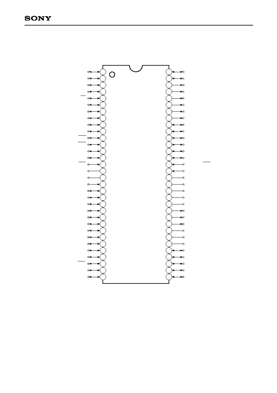
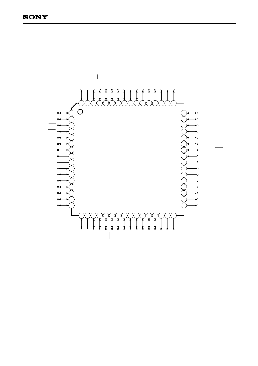
Pin Assignment (Top View) 64-pin SDIP
Note) 1. NC (Pins 38, 39, 40, 44 and 46) are left open.
2. Vss (Pins 16 and 48) are both connected to GND.
3. Pin 45 is the NC pin. However, connect it to V
DD
because it is the
EXLC pin (input) for the piggyback/evaluator and OTP devices.
4
CXP86608/86612/86616
V
SS
V
DD
NC
NC
NC
PE4
PE5
PE6
NC
NC
PE1
PE2/TEX/INT0
PE3/TX
PF3/PWM3
PF4/SCL0
PF5/SCL1
PF6/SDA0
PF7/SDA1
PE0/TO/ADJ
40
39
38
37
36
35
34
33
41
42
43
44
45
46
47
48
49
50
51
PF2/PWM2
PF1/PWM1
PF0/PWM0
PC7
PC6
PC5
PC4
PC3
PC2
PC1
PC0
PD7/EC
PD6/RMC
52
53
54
55
56
57
58
59
60
63
64
61
62
NC
PB0
PB1
PB2
PG3
PG4
PG5
PG6
PG7/INT1
PB3
PB4
PB5
PB6
31 32
20 21 22 23 24 25 26 27 28 29 30
PD4
PD5
PD3/SI
PD2/SO
PD1/SCK
PD0/INT2
PA7
PA6
RST
V
SS
PA0/AN0
XTAL
EXTAL
PA5/AN5
PA4/AN4
PA3/AN3
PA2/AN2
PA1/AN1
PB7
2
3
4
5
6
7
8
9
10
11
12
13
14
15
16
17
18
19
1
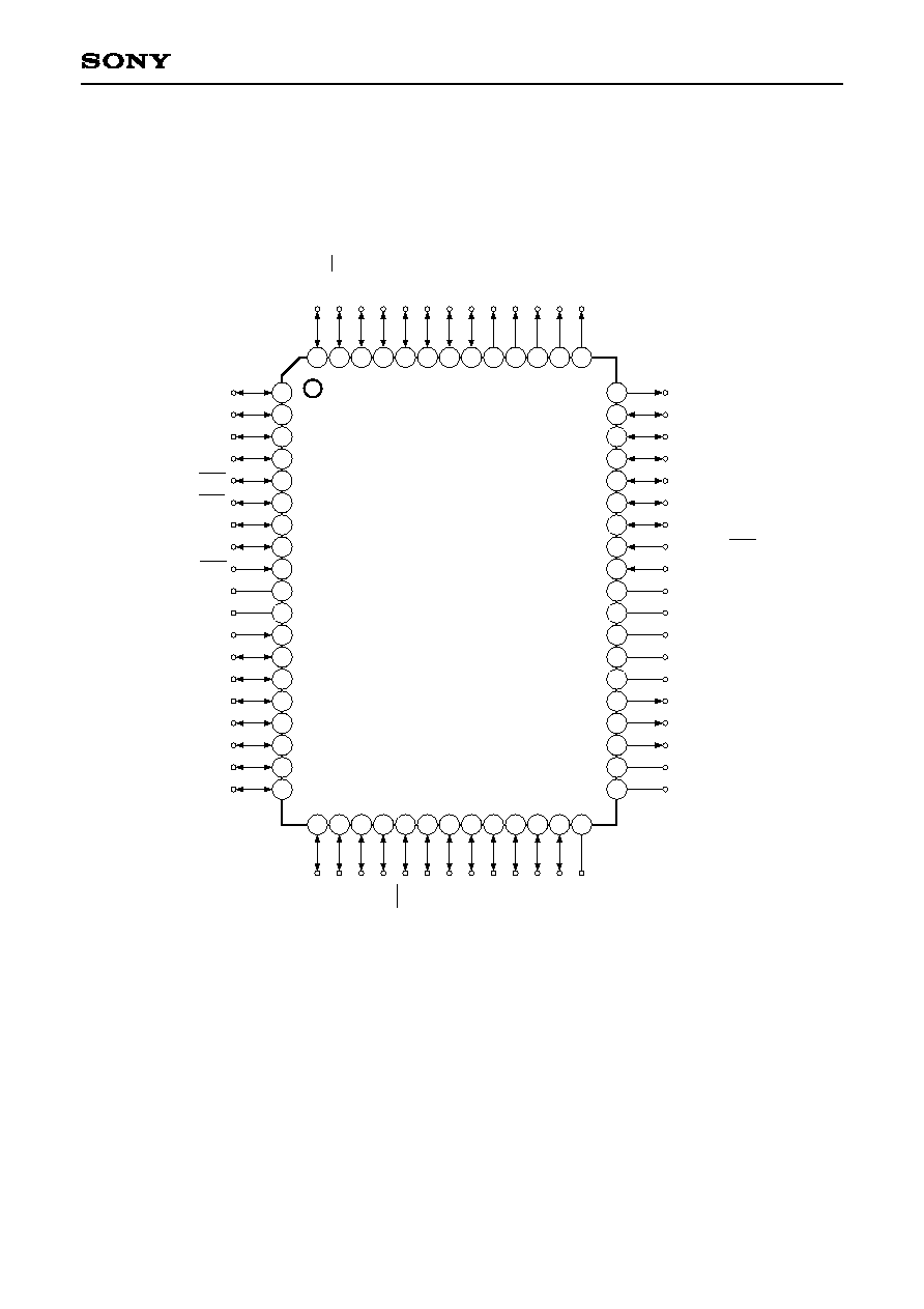
Pin Assignment (Top View) 64-pin QFP
Note) 1. NC (Pins 32, 33, 34, 38 and 40) are left open.
2. Vss (Pins 10 and 42) are both connected to GND.
3. Pin 39 is the NC pin. However, connect it to V
DD
because it is the
EXLC pin (input) for the piggyback/evaluator and OTP devices.
5
CXP86608/86612/86616
PD5
PD4
PF3/PWM3
V
SS
V
DD
NC
NC
NC
PE4
PE5
PE6
PE1
PE2/TEX/INT0
PE3/TX
PF4/SCL0
PF5/SCL1
PF6/SDA0
PF7/SDA1
PE0/TO/ADJ
40
39
38
37
36
35
34
33
41
42
43
44
45
46
47
48
49
50
51
PF2/PWM2
PF1/PWM1
PF0/PWM0
PC7
PC6
PC5
PC4
PC3
PC2
PC1
PC0
PD7/EC
PD6/RMC
52
53
54
55
56
57
58
59
60
63
64
61
62
NC
NC
NC
PB0
PB1
PB2
PG3
PG4
PG5
PG6
PG7/INT1
PB3
PB4
31 32
20 21 22 23 24 25 26 27 28 29 30
PD2/SO
PD3/SI
PD1/SCK
PD0/INT2
PA7
PA6
RST
V
SS
XTAL
EXTAL
PA5/AN5
PA4/AN4
PA3/AN3
PA2/AN2
2
3
4
5
6
7
8
9
10
11
12
13
14
15
16
17 18 19
1
PB5
PB6
PB7
PA1/AN1
PA0/AN0
Pin Assignment (Top View) 64-pin LQFP
Note) 1. NC (Pins 30, 31, 32, 36 and 38) are left open.
2. Vss (Pins 8 and 40) are both connected to GND.
3. Pin 37 is the NC pin. However, connect it to V
DD
because it is the
EXLC pin (input) for the piggyback/evaluator and OTP devices.
6
CXP86608/86612/86616
(Port A)
8-bit I/O port.
I/O can be set in a
unit of single bits.
(8 pins)
(Port B)
8-bit I/O port. I/O can be set in a unit of single bits.
(8 pins)
(Port C)
Lower 6 bits are I/O ports; I/O can be set in a unit of single bits. Upper 2bits
are output port and large current (12mA) N-channel open drain output.
Upper 2 bits are medium voltage drive (12V), lower 6 bits are 5V drive.
(8 pins)
(Port D)
8-bit I/O port.
I/O can be set in a
unit of single bits.
Can drive 12mA
sink current.
(8 pins)
(Port E)
Bits 0 and 1 are I/O
port; I/O can be set
in a unit of single.
Bits 2 and 3 are
input port.
Bits 4, 5 and 6
are output port.
(7 pins)
Pin Description
Symbol
PA0/AN0
to
PA5/AN5
PA6 to PA7
PB0 to PB7
PC6 to PC7
PD0/INT2
PD1/SCK
PD2/SO
PD3/SI
PD4 to PD5
PD6/RMC
PD7/EC
PE0/TO/ADJ
PE1
PE2/TEX/INT0
PE3/TX
PE4 to PE6
I/O/
Analog input
I/O
I/O
Output
I/O/Input
I/O/I/O
I/O/Output
I/O/Input
I/O
I/O/Input
I/O/Input
I/O/Output/
Output
I/O
Input/Input/
Input
Input/Output
Output
I/O
Description
Analog inputs to A/D converter.
(6 pins)
External interruption request input.
Active at the falling edge.
Serial clock I/O.
Serial data output.
Serial data input.
Remote control reception circuit input.
External event input for timer/counter.
Rectangular wave output
for 8-bit timer/counter.
Connects a crystal for
32kHz timer/counter
clock oscillation. When
used as an event
counter, input to TEX pin
and leave TX pin open.
32kHz oscillation
frequency dividing output.
External interruption
request input. Active at
the falling edge
PC0 to PC5
I/O
7
CXP86608/86612/86616
(Port F)
8-bit output port
and large current
(12mA) N-channel
open drain output.
Lower 4 bits are
medium voltage
drive (12V); upper
4 bits are 5V drive.
(8 pins)
(Port G)
5-bit I/O port. I/O can be set in a unit of single bits.
(5 pins)
Connects a crystal for system clock oscillation. When a clock is
supplied externally, input to EXTAL pin and input a reversed phase
clock to XTAL pin.
System reset; active at Low level.
No connected. See Note of Pin Assignment.
Positive power supply.
GND. Connect two Vss pins to GND.
8-bit PWM output.
(4 pins)
Symbol
PF0/PWM0 to
PF3/PWM3
PG3 to PG6
PG7/INT1
EXTAL
XTAL
RST
NC
V
DD
V
SS
Output/Output
I/O
I/O/Input
Input
Output
Input
I/O
Description
External interruption request input.
Active at the falling edge.
PF4/SCL0 to
PF5/SCL1
PF6/SDA0 to
PF7/SDA1
Output/I/O
Output/I/O
I
2
C bus interface transfer clock I/O.
(2 pins)
I
2
C bus interface transfer data I/O.
(2 pins)
8
CXP86608/86612/86616
Port A data
Port A direction
IP
RD (Port A)
Data bus
"0" after reset
Port A function selection
"0" after reset
A/D converter
Input multiplexer
Input protection
circuit
Port A data
Port A direction
IP
RD (Port A)
Data bus
"0" after reset
Schmitt input
Ports B, C, G data
Ports B, C, G direction
IP
RD (Ports B, C, G)
Data bus
INT1
"0" after reset
Schmitt input
only for PG7
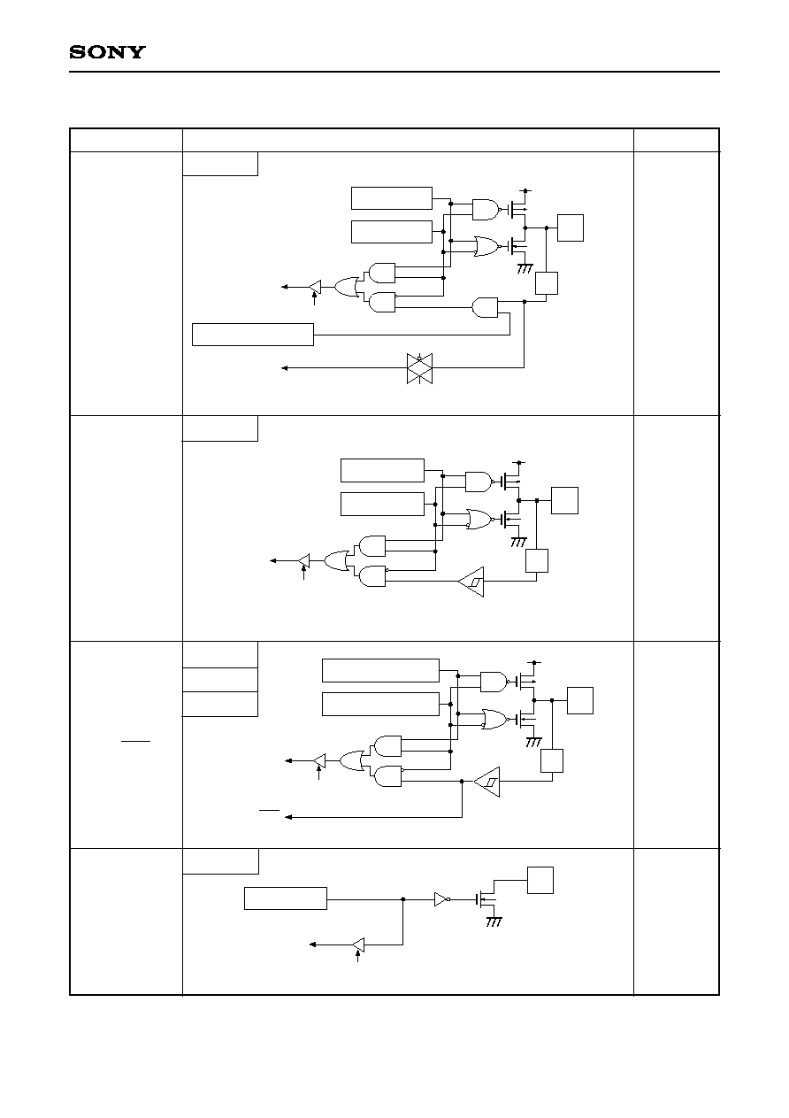
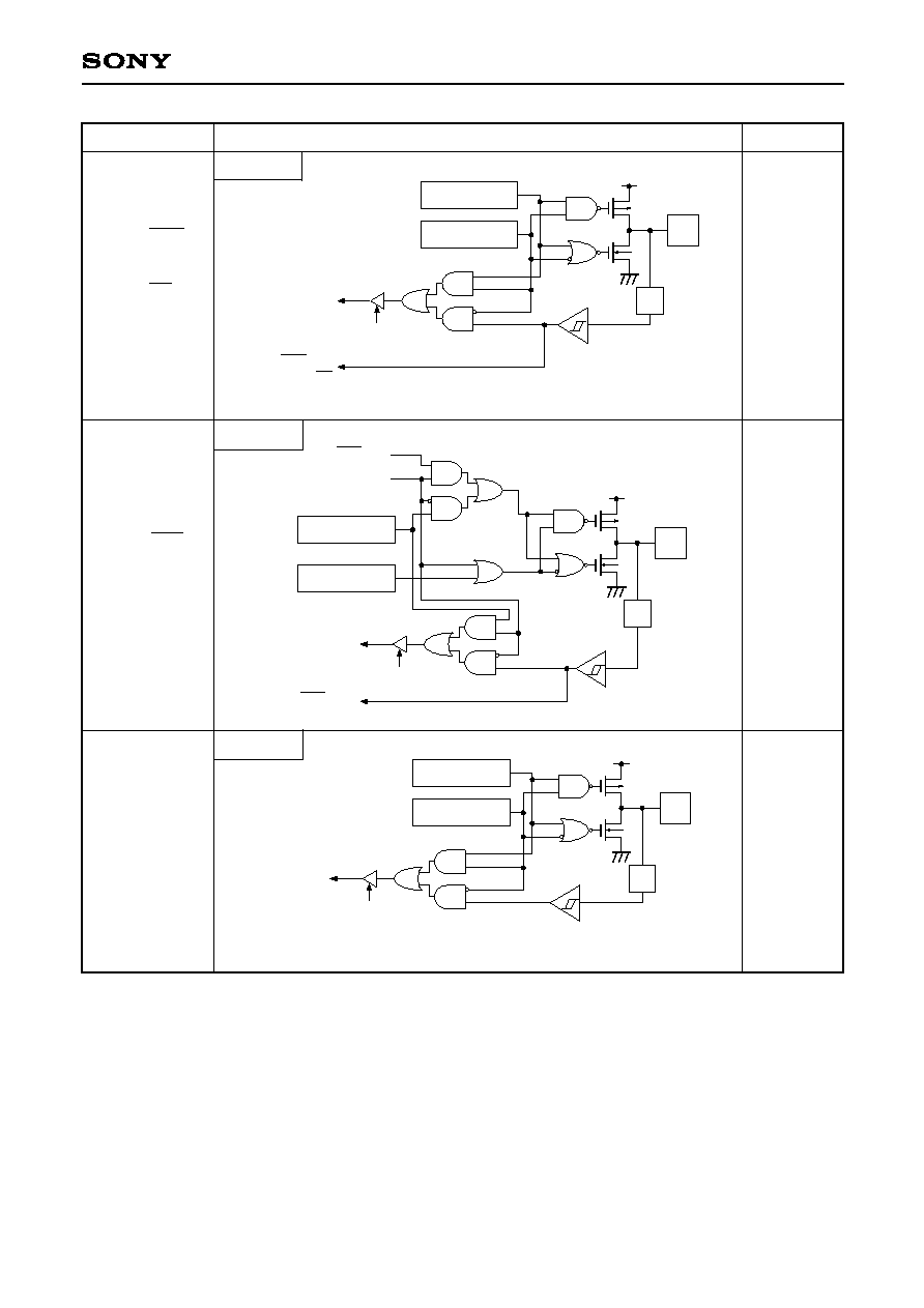
Input/Output Circuit Formats for Pins
Port A
Port A
Port B
Port C
6 pins
2 pins
19 pins
Hi-Z
Hi-Z
Hi-Z
Pin
After reset
Circuit format
PA6
PA7
PC6
PC7
PA0/AN0
to
PA5/AN5
Port G
PB0 to PB7
PC0 to PC5
PG3 to PG6
PG7/INT1
Port C data
Data bus
RD (Port C)
12V drive
Large current 12mA
Port C
2 pins
Hi-Z
9
CXP86608/86612/86616
Port D data
Port D direction
IP
RD (Port D)
Data bus
INT2, SI,
RMC, EC
"0" after reset
Schmitt input
Large current 12mA
Port D data
Port D direction
IP
RD (Port D)
Data bus
"0" after reset
Schmitt input
only for PD1
SCK, SO
SIO output enable
SCK only
Large current 12mA
Port D
Port D
4 pins
2 pins
Hi-Z
Hi-Z
PD1/SCK
PD2/SO
PD0/INT2
PD3/SI
PD6/RMC
PD7/EC
Port D data
Port D direction
IP
RD (Port D)
Data bus
"0" after reset
Schmitt input
Large current 12mA
Port D
2 pins
PD4
PD5
Hi-Z
Pin
After reset
Circuit format
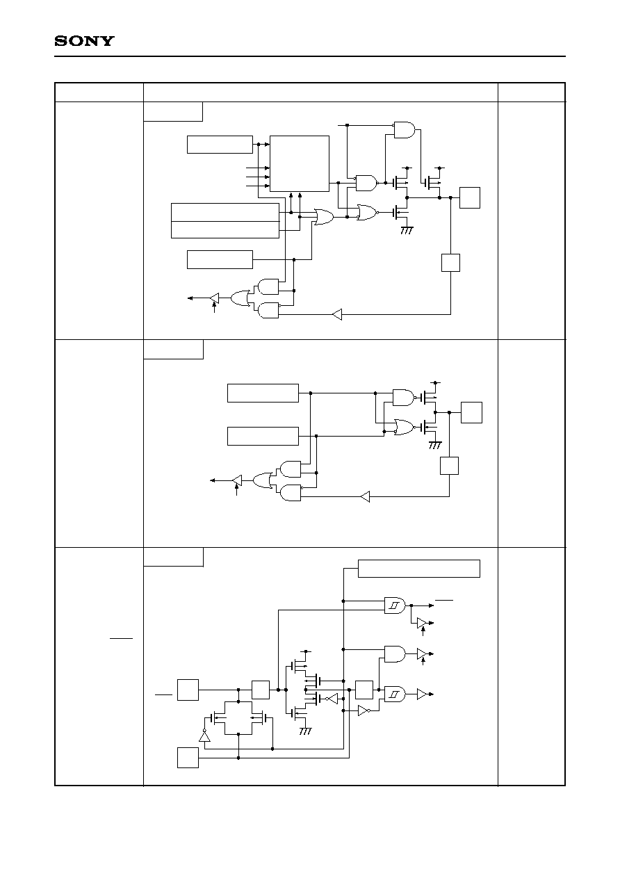
10
CXP86608/86612/86616
IP
IP
32kHz oscillation circuit control
RD (Port E)
Schmitt input
Schmitt input
Clock input
Data bus
Data bus
INT0
"1" after reset
PE2/
TEX/
INT0
PE3/
TX
RD (Port E)
Port E data
Port E direction
IP
RD (Port E)
Data bus
"1" after reset
"1" after reset
Port E
Port E
1 pin
2 pins
PE2/TEX/INT0
PE3/TX
High level
Oscillation
stop
Port input
PE1
Port E data
"1" after reset
TO
ADJ16K
ADJ2K
1
1
01
00
10
11
MPX
Data bus
Port E direction
"1" after reset
Port E function selection (lower)
"00" after reset
IP
Port E function selection (upper)
Internal reset signal
2
1
ADJ signals are frequency
dividing outputs for 32kHz
oscillation frequency
adjustment.
ADJ2K provides usage as
buzzer output.
2
Pull-up transistor approx. 150k
RD (Port E)
Port E
1 pin
High level
(with the
resistor of
pull-up
transistor ON
when reset)
PE0/TO/ADJ
Pin
After reset
Circuit format
11
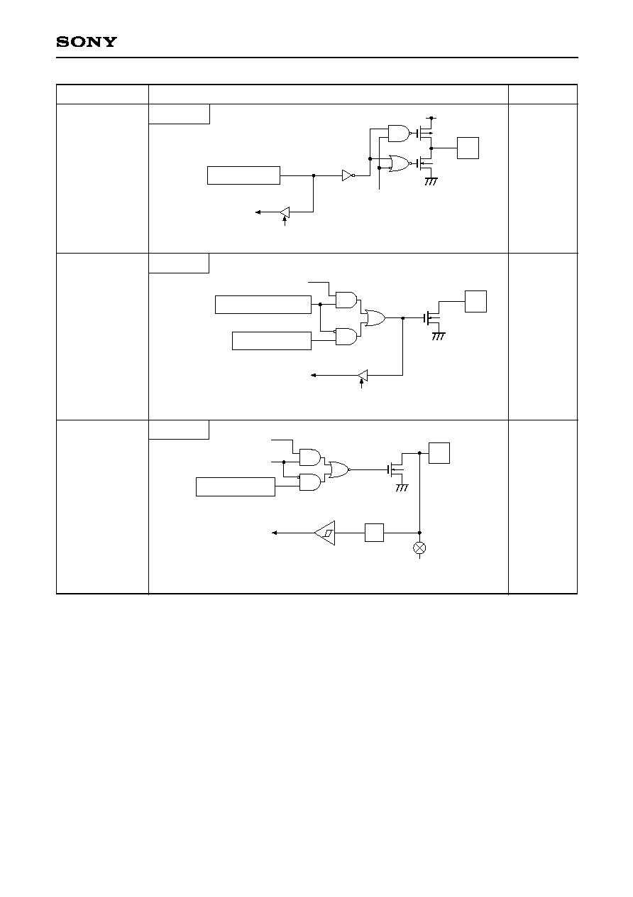
CXP86608/86612/86616
4 pins
Hi-Z
I
2
C output enable
Port F data
"1" after reset
SCL, SDA
SCL, SDA
(I
2
C circuit)
IP
Schmitt input
Large current 12mA
To internal I
2
C pins
(SCL1 for SCL0)
BUS SW
Port F
PF4/SCL0
PF5/SCL1
PF6/SDA0
PF7/SDA1
3 pins
Hi-Z
PE4
PE5
PE6
Port E data
Output becomes active from
high impedance by data writing
to port register.
Data bus
RD (Port E)
Port E
Port F data
Port F function selection
"0" after reset
"1" after reset
PWM0 to PWM3
12V drive
Large current 12mA
RD (Port F)
Data bus
Port F
4 pins
PF0/PWM0
to
PF3/PWM3
Hi-Z
Pin
After reset
Circuit format
12
CXP86608/86612/86616
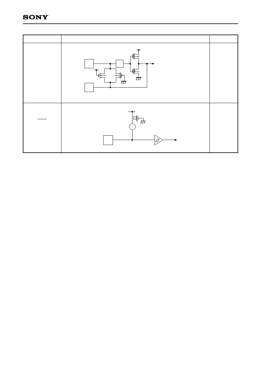
IP
EXTAL
XTAL
· Diagram shows the circuit
composition during oscillation.
· Feedback resistor is removed
during stop.
(This device does not enter the
stop mode.)
Schmitt input
Pull-up resistor
OP
Mask option
2 pins
EXTAL
XTAL
1 pin
RST
Oscillation
Low level
(when reset)
Pin
After reset
Circuit format
13
CXP86608/86612/86616
1
V
IN
and V
OUT
should not exceed V
DD
+ 0.3V.
2
The large current output port is Port C (PC6, PC7), Port D (PD) and Port F (PF).
Note) Usage exceeding absolute maximum ratings may permanently impair the LSI. Normal operation should
be conducted under the recommended operating conditions. Exceeding those conditions may adversely
affect the reliability of the LSI.
V
DD
V
IN
V
OUT
V
OUTP
I
OH
I
OH
I
OL
I
OLC
I
OL
Topr
Tstg
P
D
0.3 to +7.0
0.3 to +7.0
1
0.3 to +7.0
1
0.3 to +15.0
5
50
15
20
130
20 to +75
55 to +150
1000
600
380
V
V
V
V
mA
mA
mA
mA
mA
°C
°C
mW
mW
mW
Total of all output pins
Ports excluding large current output (value per pin)
Large current output ports (value per pin
2
)
Total of all output pins
SDIP-64P-01
QFP-64P-L01
LQFP-64P-L01
Item
Symbol
Ratings
Unit
Remarks
Absolute Maximum Ratings
(Vss = 0V reference)
Supply voltage
High level input
voltage
Low level input
voltage
Operating temperature
5.5
5.5
5.5
--
V
DD
V
DD
V
DD
+ 0.3
0.3V
DD
0.2V
DD
0.4
+75
V
V
V
V
V
V
V
V
V
V
°C
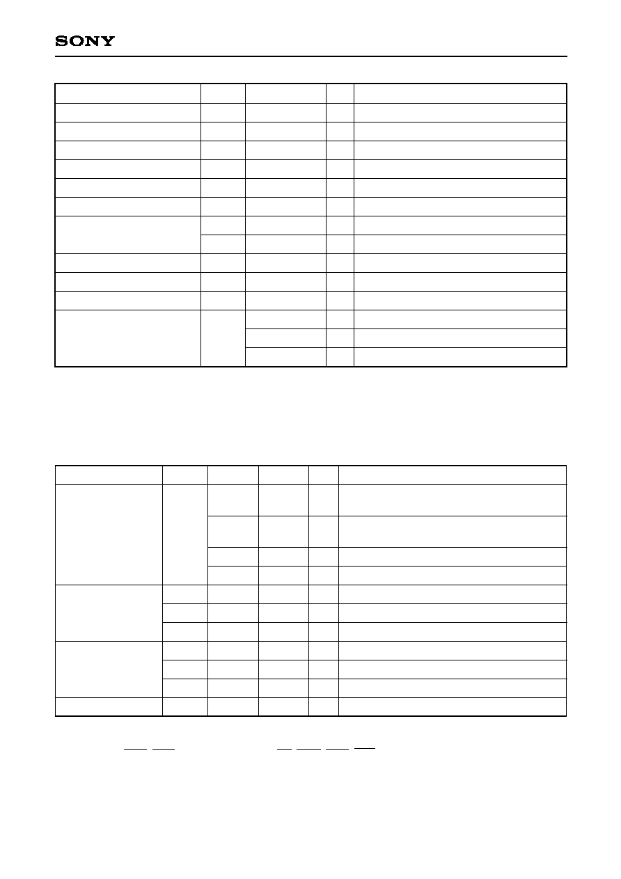
Item
Symbol
Min.
Max.
Unit
Remarks
3.0
3.0
2.7
--
0.7V
DD
0.8V
DD
V
DD
0.4
0
0
0.3
20
V
IH
V
IHS
V
IHEX
V
IL
V
ILS
V
ILEX
Topr
Guaranteed operation range for 1/2 and 1/4
frequency dividing clocks
Guaranteed operation range for 1/16 frequency
dividing clock or sleep mode
Guaranteed operation range for TEX
Guaranteed data hold range for stop
1
2
3
EXTAL pin
4
, TEX pin
5
2
3
EXTAL pin
4
, TEX pin
5
V
DD
1
This device does not enter the stop mode.
2
PA0 to PA5, PB0 to PB7, PC0 to PC5, PD2, PE0, PE1, PE3, PG3 to PG6, SCL0, SCL1, SDA0, SDA1 pins
3
PA6, PA7, INT2, SCK, SI, PD4, PD5, RMC, EC, INT0, INT1, RST pins
4
Specifies only during external clock input.
5
Specifies only during external event count input.
Recommended Operating Conditions
(Vss = 0V reference)
Supply voltage
Input voltage
Output voltage
Medium drive output voltage
High level output current
High level total output current
Low level output current
Low level total output current
Operating temperature
Storage temperature
Allowable power dissipation
14
CXP86608/86612/86616
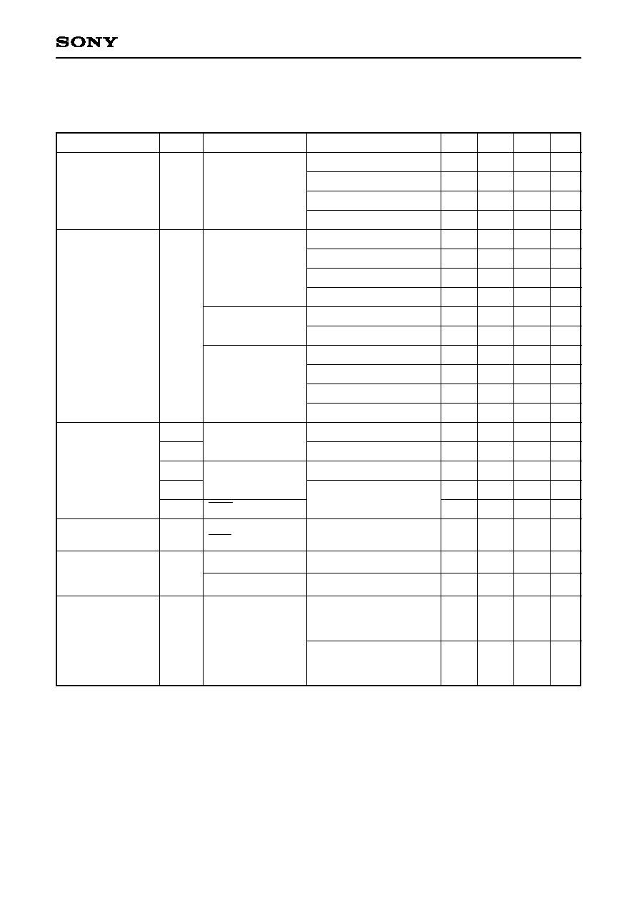
Item
Symbol
Pins
Conditions
Min.
Typ.
Max.
Unit
High level output
voltage
Low level output
voltage
Input current
I/O leakage current
Open drain I/O
leakage current
(in N-ch Tr off state)
I
2
C bus switch
connection
impedance
(in output Tr off state)
V
OH
V
OL
I
IHE
I
ILE
I
IHT
I
ILT
I
ILR
I
IZ
I
LOH
R
BS
PA, PB, PC0 to PC5,
PD, PE0 to PE1,
PE4 to PE6, PG
PA to PD, PE0 to PE1,
PE4 to PE6, PF0 to PF3,
PG
PC6, PC7, PD, PF
PF4 to PF7
(SCL0, SCL1,
SDA0, SDA1)
EXTAL
TEX
RST
1
PA to PE, PG,
RST
1
PC6, PC7, PF0 to PF3
PF4 to PF7
SCL0: SCL1
SDA0: SDA1
V
DD
= 4.5V, I
OH
= 0.5mA
V
DD
= 4.5V, I
OH
= 1.2mA
V
DD
= 3.0V, I
OH
= 0.15mA
V
DD
= 3.0V, I
OH
= 0.5mA
V
DD
= 4.5V, I
OL
= 1.8mA
V
DD
= 4.5V, I
OL
= 3.6mA
V
DD
= 3.0V, I
OL
= 1.2mA
V
DD
= 3.0V, I
OL
= 1.6mA
V
DD
= 4.5V, I
OL
= 12.0mA
V
DD
= 3.0V, I
OL
= 5.0mA
V
DD
= 4.5V, I
OL
= 3.0mA
V
DD
= 4.5V, I
OL
= 4.0mA
V
DD
= 3.0V, I
OL
= 2.0mA
V
DD
= 3.0V, I
OL
= 2.5mA
V
DD
= 5.5V, V
IH
= 5.5V
V
DD
= 5.5V, V
IL
= 0.4V
V
DD
= 5.5V, V
IH
= 5.5V
V
DD
= 5.5V, V
IL
= 0.4V
V
DD
= 5.5V,
V
I
= 0, 5.5V
V
DD
= 5.5V, V
OH
= 12.0V
V
DD
= 5.5V, V
OH
= 5.5V
V
DD
= 4.5V
V
SCL0
= V
SCL1
= 2.25V
V
SDA0
= V
SDA1
= 2.25V
V
DD
= 3.0V
V
SCL0
= V
SCL1
= 1.5V
V
SDA0
= V
SDA1
= 1.5V
4.0
3.5
2.7
2.0
0.5
0.5
0.1
0.1
1.5
0.4
0.6
0.3
0.5
1.5
1.0
0.4
0.6
0.3
0.5
40
40
10
10
400
±10
50
10
120
400
V
V
V
V
V
V
V
V
V
V
V
V
V
V
µA
µA
µA
µA
µA
µA
µA
µA
Electrical Characteristics
DC characteristics
(Ta = 20 to +75°C, Vss = 0V reference)
15
CXP86608/86612/86616
1
For RST pin, specifies the input current when pull-up resistor is selected, and specifies the leakage current
when non-resistor is selected.
2
When all output pins are left open.
3
This device does not enter the stop mode.
Item
Symbol
Pins
Conditions
Min.
Typ.
Max.
Unit
Supply current
2
Input capacitance
I
DD1
I
DD2
I
DDS1
I
DDS2
I
DDS3
C
IN
V
DD
PA to PD, PE0 to PE3,
PF4 to PF7, PG3 to PG7,
EXTAL, TEX, RST
1/2 frequency dividing
clock operation
V
DD
= 5.5V, 16MHz
crystal oscillation
(C
1
= C
2
= 15pF)
V
DD
= 3.6V, 8MHz
crystal oscillation
(C
1
= C
2
= 15pF)
V
DD
= 3.3V, 32kHz
crystal oscillation
(C
1
= C
2
= 47pF)
Sleep mode
V
DD
= 5.5V, 16MHz
crystal oscillation
(C
1
= C
2
= 15pF)
V
DD
= 3.6V, 8MHz
crystal oscillation
(C
1
= C
2
= 15pF)
V
DD
= 3.3V, 32kHz
crystal oscillation
(C
1
= C
2
= 47pF)
Stop mode
3
V
DD
= 5.5V, termination
of 16MHz and 32kHz
oscillation
Clock 1MHz
0V for no measured pins
--
18
4.5
30
1.2
0.22
12
--
10
28
9.0
80
2.1
0.4
35
--
20
mA
mA
µA
mA
mA
µA
µA
pF
16
CXP86608/86612/86616
1
Indicates three values according to the contents of the clock control register (CLC: 00FEh) upper 2 bits (CPU
clock selection).
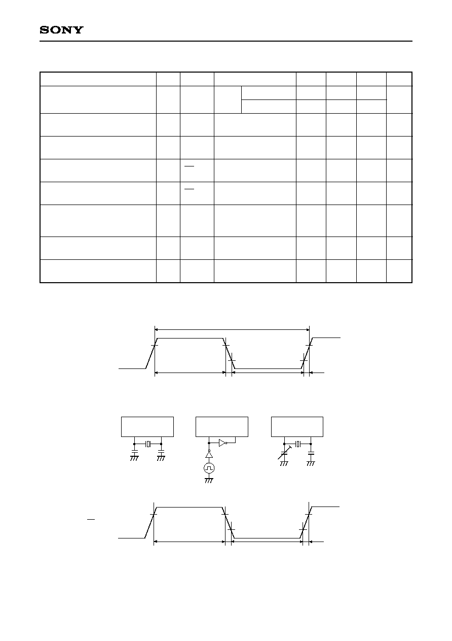
t
sys [ns] = 2000/fc (Upper 2 bits = "00"), 4000/fc (Upper 2 bits = "01"), 16000/fc (Upper 2 bits = "11")
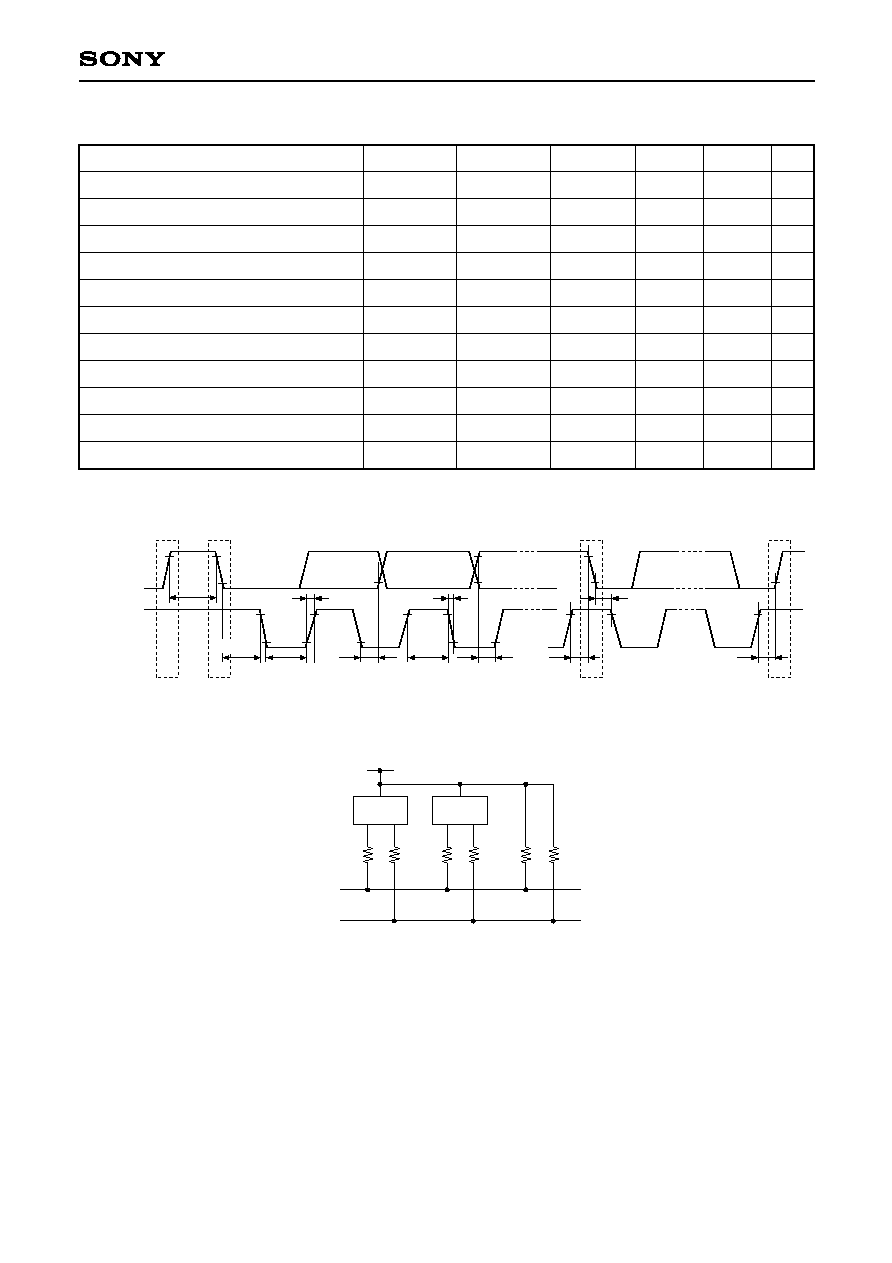
EXTAL
t
XH
t
XL
t
CF
t
CR
0.4V
V
DD
0.4V
1/fc
Crystal oscillation
Ceramic oscillation
EXTAL
XTAL
External clock
EXTAL
XTAL
74HC04
C
1
C
2
32kHz clock applied condition
Crystal oscillation
TEX
TX
C
1
C
2
TEX
EC
t
EH
t
EL
t
EF
t
ER
0.2V
DD
0.8V
DD
t
TH
t
TL
t
TF
t
TR
AC Characteristics
(1) Clock timing
(Ta = 20 to +75°C, V
DD
= 3.0 to 5.5V, Vss = 0V reference)
Fig.2. Clock applied conditions
Fig. 1. Clock timing
Fig. 3. Event count clock timing
System clock frequency
System clock input pulse width
System clock input rise and fall
times
Event count input clock pulse
width
Event count input clock rise and
fall times
System clock frequency
Event count input clock input
pulse width
Event count input clock rise and
fall times
f
C
t
XL
,
t
XH
t
CR
,
t
CF
t
EH
,
t
EL
t
ER
,
t
EF
f
C
t
TL
,
t
TH
t
TR
,
t
TF
XTAL
EXTAL
EXTAL
EXTAL
EC
EC
TEX
TX
TEX
TEX
MHz
ns
ns
ns
ms
kHz
µs
ms
Item
Symbol
Pins
Conditions
Min.
Unit
Fig. 1,
Fig. 2
Fig. 1, Fig. 2
External clock drive
Fig. 1, Fig. 2
External clock drive
Fig. 3
Fig. 3
V
DD
= 2.7 to 5.5V
Fig. 2 (32kHz clock
applied conditions)
Fig. 3
Fig. 3
1
1
28
4
t
sys
1
10
Typ.
32.768
Max.
16
8
200
20
20
V
DD
= 4.5 to 5.5V
V
DD
= 3 to 3.6V
17
CXP86608/86612/86616
(2) Serial transfer
(Ta = 20 to +75°C, V
DD
= 4.5 to 5.5V, Vss = 0V reference)
Item
SCK cycle time
t
KCY
SCK
Input mode
Output mode
SCK input mode
SCK output mode
SCK input mode
SCK output mode
SCK input mode
SCK output mode
SCK input mode
SCK output mode
1000
8000/fc
400
4000/fc 50
100
200
200
100
200
100
ns
ns
ns
ns
ns
ns
ns
ns
ns
ns
SCK
SI
SI
SO
t
KH
t
KL
t
SIK
t
KSI
t
KSO
SCK High and Low level
width
SI input setup time
(for SCK
)
SI hold time (for SCK
)
SCK
SO delay time
Symbol
Pins
Conditions
Min.
Max.
Unit
Note) The load of SCK output mode and SO output delay time is 50pF + 1TTL.
(Ta = 20 to +75°C, V
DD
= 3.0 to 3.6V, Vss = 0V reference)
Item
SCK cycle time
t
KCY
SCK
Input mode
Output mode
SCK input mode
SCK output mode
SCK input mode
SCK output mode
SCK input mode
SCK output mode
SCK input mode
SCK output mode
1000
8000/fc
400
4000/fc 50
100
200
200
100
400
200
ns
ns
ns
ns
ns
ns
ns
ns
ns
ns
SCK
SI
SI
SO
t
KH
t
KL
t
SIK
t
KSI
t
KSO
SCK High and Low level
width
SI input setup time
(for SCK
)
SI hold time (for SCK
)
SCK
SO delay time
Symbol
Pins
Conditions
Min.
Max.
Unit
Note) The load of SCK output mode and SO output delay time is 50pF + 1TTL.
18
CXP86608/86612/86616
Fig. 4. Serial transfer timing
0.2V
DD
0.8V
DD
t
KL
t
KH
SO
t
KCY
t
SIK
t
KSI
0.2V
DD
0.8V
DD
t
KSO
0.2V
DD
0.8V
DD
Output data
Input data
SI
SCK
19
CXP86608/86612/86616
Resolution
Linearity error
Zero transition
voltage
Full-scale transition
voltage
Linearity error
Zero transition
voltage
Full-scale transition
voltage
Conversion time
Sampling time
Analog input voltage
V
ZT
1
V
FT
2
V
ZT
1
V
FT
2
t
CONV
t
SAMP
V
IAN
AN0 to AN5
Ta = 25°C
V
DD
= 5.0V
Vss = 0V
Ta = 25°C
V
DD
= 3.3V
Vss = 0V
10
4910
10
3215
26/f
ADC
3
6/f
ADC
3
0
10
4970
6.5
3280
8
±3
70
5030
±5
70
3345
V
DD
Bits
LSB
mV
mV
LSB
mV
mV
µs
µs
V
Item
Symbol
Pins
Conditions
Min.
Typ.
Max.
Unit
(3) A/D converter characteristics
(Ta = 20 to +75°C, V
DD
= 3.0 to 5.5V, Vss = 0V reference)
Linearity error
V
ZT
V
FT
Analog input
FFh
FEh
01h
00h
Digital conversion value
Fig. 5. Definitions of A/D converter terms
1
V
ZT
: Value at which the digital conversion value changes
from 00h to 01h and vice versa.
2
V
FT
: Value at which the digital conversion value changes
from FEh to FFh and vice versa.
3
f
ADC
indicates the below values due to the contents of bit 6
(CKS) of the A/D control register (ADC: 00F6h):
f
ADC
= fc (CKS = "0"), fc/2 (CKS = "1")
20
CXP86608/86612/86616
External interruption High,
Low level width
Reset input Low level width
INT0
INT1
INT2
RST
1
32/fc
µs
µs
Item
Symbol
Pins
Conditions
Min.
Max.
Unit
t
IH
t
IL
t
RSL
(4) Interruption, reset input
(Ta = 20 to +75°C, V
DD
= 3.0 to 5.5V, Vss = 0V reference)
0.2V
DD
0.8V
DD
t
IH
t
IL
INT0
INT1
INT2
(falling edge)
Fig. 6. Interruption input timing
t
RSL
0.2V
DD
RST
Fig. 7. RST input timing
21
CXP86608/86612/86616
(5) I
2
C bus timing
(Ta = 20 to +75°C, V
DD
= 3.0 to 5.5V, Vss = 0V reference)
Item
SCL clock frequency
Bus-free time before starting transfer
Hold time for starting transfer
Clock Low level width
Clock High level width
Setup time for repeated transfers
Data hold time
Data setup time
SDA, SCL rise time
SDA, SCL fall time
Setup time for transfer completion
f
SLC
t
BUF
t
HD; STA
t
LOW
t
HIGH
t
SU; STA
t
HD; DAT
t
SU; DAT
t
R
t
F
t
SU; STO
SCL
SDA, SCL
SDA, SCL
SCL
SCL
SDA, SCL
SDA, SCL
SDA, SCL
SDA, SCL
SDA, SCL
SDA, SCL
0
4.7
4.0
4.7
4.0
4.7
0
1
250
4.7
100
1
300
kHz
µs
µs
µs
µs
µs
µs
ns
µs
ns
µs
Symbol
Pins
Conditions
Min.
Max.
Unit
1
The data hold time should be 300ns or more because the SCL rise time (300ns Max.) is not included in it.
Fig. 8. I
2
C bus transfer timing
P
St
t
SU; STO
t
SU; STA
t
HD; STA
t
SU; DAT
t
HIGH
t
HD; DAT
t
F
t
R
t
LOW
t
HD; STA
S
P
t
BUF
SDA
SCL
Fig. 9. I
2
C device recommended circuit
I
2
C
device
I
2
C
device
R
S
R
S
R
S
R
S
R
P
R
P
SDA0
(or SDA1)
SCL0
(or SCL1)
· A pull-up resistor (Rp) must be connected to SDA0 (or SDA1) and SCL0 (or SCL1).
· The SDA0 (or SDA1) and SCL0 (or SCL1) series resistance (Rs = 300
or less) can be used to reduce the
spike noise caused by CRT flashover.
22
CXP86608/86612/86616
Appendix
C
2
Rd
EXTAL
XTAL
C
1
(i) Main clock
TEX
TX
C
1
C
2
Rd
(iii) Sub clock
Rd
EXTAL
XTAL
C
1
C
2
(ii) Main clock
Reset pin pull-up resistor
Non-existent
Existent
Item
Content
Mask Option Table
Manufacture
RIVER
ELETEC
CORPORATION
MURATA MFG
CO., LTD.
CSA10.0MTZ
CSA12.0MTZ
CSA16.00MXZ040
CST10.0MTW
CST12.0MTW
CST16.00MXW0C1
KINSEKI LTD.
Model
HC-49/U03
HC-49/U (-S)
P3
fc (MHz)
10.0
12.0
16.0
10.0
12.0
16.0
8.0
12.0
16.0
8.0
12.0
16.0
30
5
30
5
18
12
10
10
5
Open
30
30
5
30
5
18
12
10
10
5
Open
33
0
1
330
1
0
1
120k
32.768kHz
(iii)
C
1
(pF)
C
2
(pF)
Rd (
)
Circuit
example
(i)
Models with an asterisk have the built-in ground capacitance (C
1
, C
2
).
1
The series resistor for XTAL (Rd = 500
or less) can reduce the effect of the noise caused by the electrostatic
discharge.
(i)
(ii)
Fig. 10. Recommended oscillation circuit
23
CXP86608/86612/86616
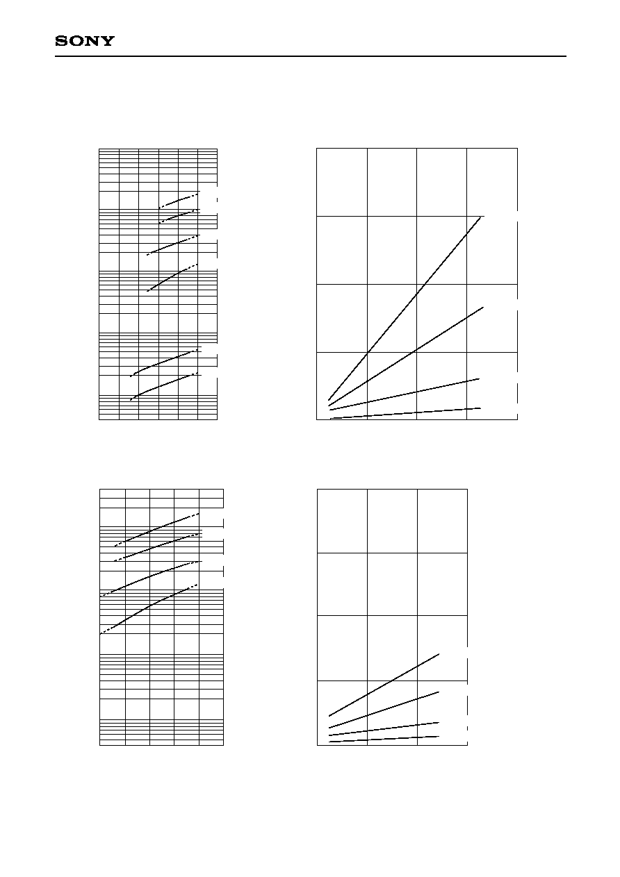
Fig. 11. Characteristic curves
I
DD
vs. V
DD
(fc = 16MHz, Ta = 25°C, Typical)
15
10
5
fc System clock [MHz]
I
DD
Supply current [mA]
I
DD
vs. fc
(V
DD
= 5V, Ta = 25°C, Typical)
3
4
5
6
0.1
1
V
DD
Supply voltage [V]
I
DD
Supply current [mA]
7
2
0.01
10
1/16 dividing mode
1/4 dividing mode
Sleep mode
100
32kHz sleep mode
32kHz operation mode
1/2 dividing mode
1/2 dividing mode
1/4 dividing mode
1/16 dividing mode
Sleep mode
10
0
5
15
0
1
I
DD
vs. V
DD
(fc = 8MHz, Ta = 25°C, Typical)
15
10
5
fc System clock [MHz]
I
DD
Supply current [mA]
I
DD
vs. fc
(V
DD
= 3.3V, Ta = 25°C, Typical)
3
4
5
6
V
DD
Supply voltage [V]
I
DD
Supply current [mA]
5.0
1/2 dividing mode
1/4 dividing mode
1/16 dividing mode
Sleep mode
10
0
5
15
0
20
20.0
10.0
0.5
1.0
1/16 dividing mode
Sleep mode
1/2 dividing mode
1/4 dividing mode
0.1
(100µA)
0.05
(50µA)
0.01
(10µA)
1
24
CXP86608/86612/86616
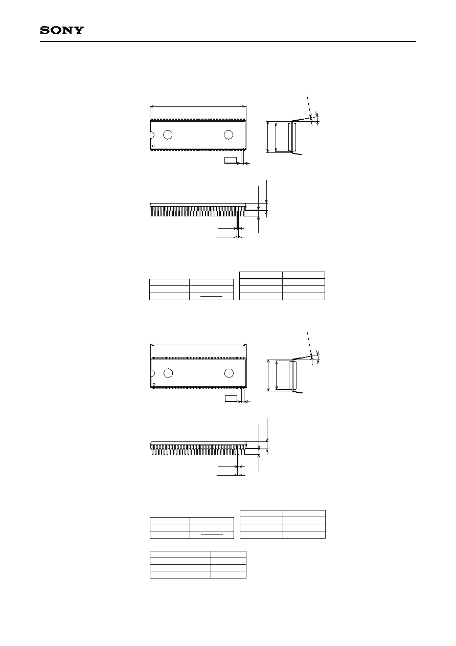
Package Outline
Unit: mm
64PIN
SDIP (PLASTIC)
MI
N
0.
5
MI
N
3.
0
4.
75 0.
1
0.9
±
0.15
0.5
±
0.1
0.
25 0.
05
+ 0.
1
17.
1
0.
1
19.
0
5
1
32
33
64
1.778
57.6 0.1
+ 0.4
PACKAGE MATERIAL
LEAD TREATMENT
LEAD MATERIAL
PACKAGE MASS
EPOXY RESIN
42/COPPER ALLOY
SONY CODE
EIAJ CODE
JEDEC CODE
SDIP-64P-01
P-SDIP64-17.1x57.6-1.778
SOLDER PLATING
8.6g
+ 0.
3
+ 0.
3
0° to 15°
PACKAGE STRUCTURE
64PIN
SDIP (PLASTIC)
MI
N
0.
5
MI
N
3.
0
4.
75
0.
1
0.9
±
0.15
0.5
±
0.1
0.
25
0.
05
+ 0.
1
17.
1
0.
1
19.
0
5
1
32
33
64
1.778
57.6 0.1
+ 0.4
PACKAGE MATERIAL
LEAD TREATMENT
LEAD MATERIAL
PACKAGE MASS
EPOXY RESIN
42/COPPER ALLOY
SONY CODE
EIAJ CODE
JEDEC CODE
SDIP-64P-01
P-SDIP64-17.1x57.6-1.778
SOLDER PLATING
8.6g
+ 0.
3
+ 0.
3
0° to 15°
PACKAGE STRUCTURE
LEAD PLATING SPECIFICATIONS
ITEM
LEAD MATERIAL
42 ALLOY
SOLDER COMPOSITION
Sn-Bi Bi:1-4wt%
PLATING THICKNESS
5-18
µ
m
SPEC.
25
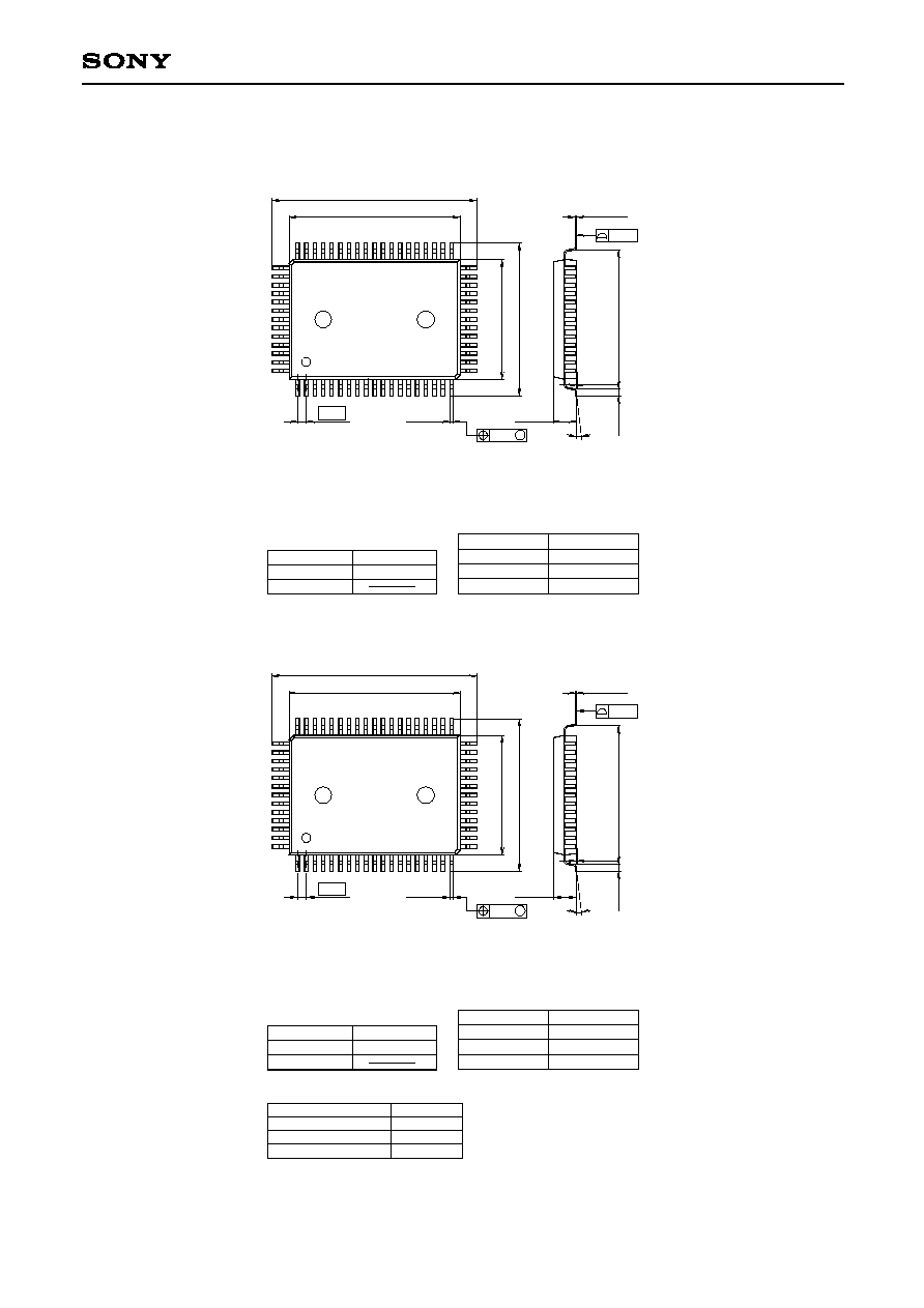
CXP86608/86612/86616
Package Outline
Unit: mm
SONY CODE
EIAJ CODE
JEDEC CODE
23.9
±
0.4
20.0 0.1
0.4 0.1
+ 0.15
14.
0
0.
1
1
19
20
32
33
51
52
64
0.15 0.05
+ 0.1
2.75 0.15
16.
3
0.1 0.05
+ 0.2
0.
8
±
0.
2
M
0.2
0.15
+ 0.4
17.9
±
0.4
+ 0.
4
+ 0.35
64PIN QFP (PLASTIC)
QFP-64P-L01
P-QFP64-14x20-1.0
PACKAGE MATERIAL
LEAD TREATMENT
LEAD MATERIAL
PACKAGE MASS
EPOXY RESIN
SOLDER PLATING
42/COPPER ALLOY
PACKAGE STRUCTURE
1.5g
1.0
0
°
to10
°
LEAD PLATING SPECIFICATIONS
ITEM
LEAD MATERIAL
42 ALLOY
SOLDER COMPOSITION
Sn-Bi Bi:1-4wt%
PLATING THICKNESS
5-18
µ
m
SPEC.
26
CXP86608/86612/86616
Sony Corporation
Package Outline
Unit: mm
SONY CODE
EIAJ CODE
JEDEC CODE
PACKAGE MATERIAL
LEAD TREATMENT
LEAD MATERIAL
PACKAGE MASS
EPOXY RESIN
42/COPPER ALLOY
PACKAGE STRUCTURE
12.0
±
0.2
10.0
±
0.1
(0.22)
b
1
16
17
32
33
48
49
64
0.1
±
0.1
0.5
±
0.2
0
°
to 10
°
64PIN LQFP (PLASTIC)
LQFP-64P-L01
P-LQFP64-10x10-0.5
0.3g
DETAIL A
0.5
±
0.2
(11.0)
A
1.5 0.1
+ 0.2
0.1
SOLDER PLATING
NOTE: Dimension "
" does not include mold protrusion.
0.13 M
0.5
b = 0.18 0.03
( 0.18 )
(0.127)
+ 0.08
0.127
0.02
+ 0.05
DETAIL B: SOLDER
LEAD PLATING SPECIFICATIONS
ITEM
LEAD MATERIAL
42 ALLOY
SOLDER COMPOSITION
Sn-Bi Bi:1-4wt%
PLATING THICKNESS
5-18
µ
m
SPEC.