CMOS 8-bit Single Chip Microcomputer
Description
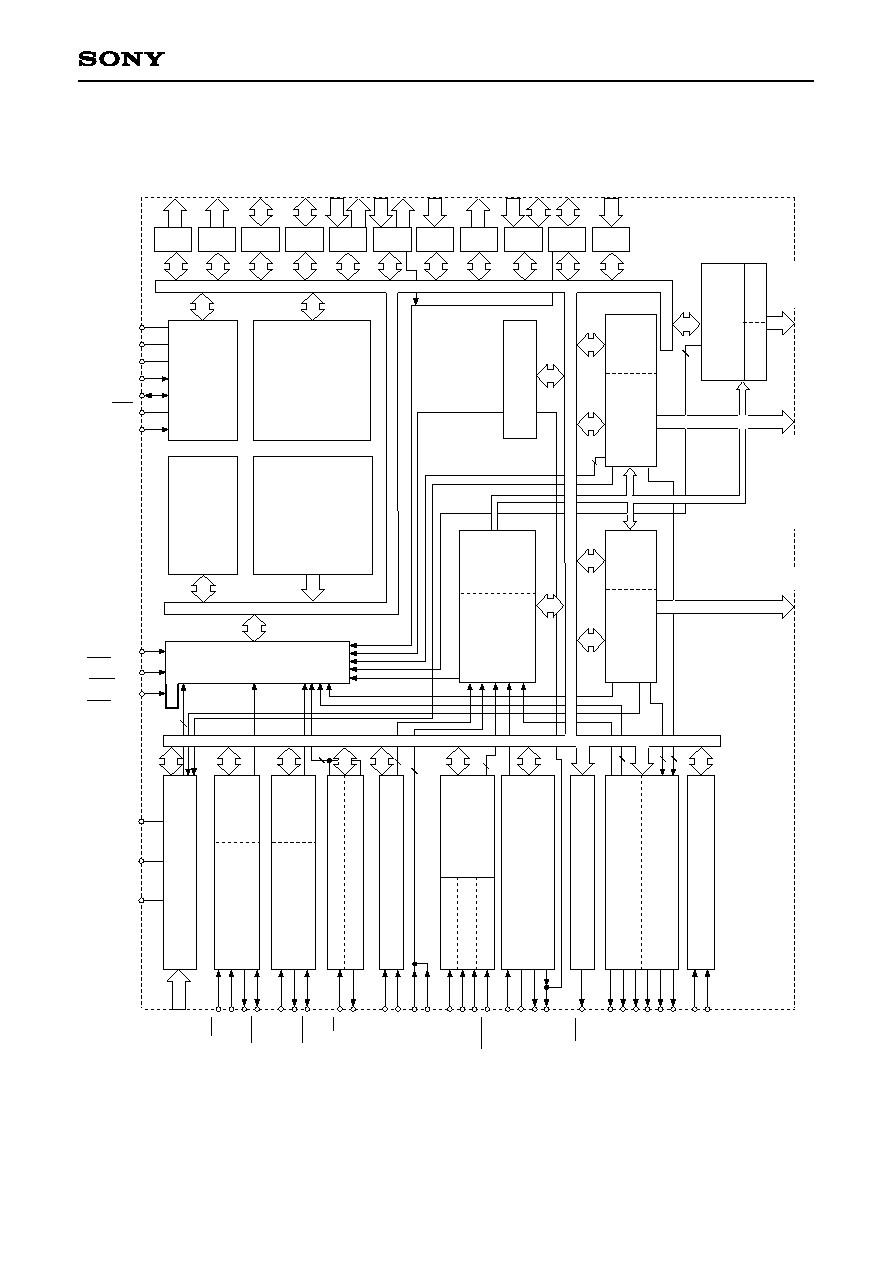
The CXP871P40 is a CMOS 8-bit microcomputer
which consists of A/D converter, serial interface (2ch
independently), timer/counter, time base timer,
vector interruption, high precision timing pattern
generation circuit (PPG 2ch independently, RTG 2ch
independently), PWM generator, general purpose
prescaler, PWM for tuner, VCR vertical sync
separation circuit and the measuring circuit which
measures signals of capstan FG and drum FG/PG
and other servo systems, as well as basic
configurations like 8-bit CPU, PROM, RAM and I/O
port. They are integrated into a single chip.
Also CXP871P40 provides power on reset
function, sleep/stop function which enables to lower
power consumption .
CXP871P40 is the PROM-incorporated version of
the CXP87132/87140 with built-in mask ROM. This
provides the additional feature of being able to write
directly into the program. Thus, it is most suitable for
evaluation use during system development and for
small-quantity production.
Features
∑ A wide instruction set (213 instructions) which covers various types of data
-- 16-bit arithmetic instruction/multiplication and division instructions/boolean bit operation instruction
∑ Minimum instruction cycle
333ns at 12MHz operation (3.0 to 5.5V)
250ns at 16MHz operation (4.5 to 5.5V)
∑ Incorporated PROM capacity
40K bytes
∑ Incorporated RAM capacity
1312 bytes
∑ Peripheral functions
-- A/D converter
8-bit, 12-channel, successive approximation system
(Conversion time: 20µs/16MHz)
-- Serial I/O
Incorporated buffer RAM (1 to 32 bytes auto transfer) 1-channel
Incorporated 8-bit and 8-stage FIFO
(1 to 8 bytes auto transfer) 1-channel
-- Timer
8-bit timer, 8-bit timer/counter, 19-bit time base timer
-- High precision timing pattern generator
PPG 19 pins 32-stage programmable
PPG 10 pins 21-stage programmable
RTG 5 pins 2-channel
-- PWM/DA gate output
PWM 12-bit, 2-channel (Repetitive frequency 62.5kHz/16MHz)
DA gate pulse 12-bit, 4-channel
-- Servo input control
Capstan FG, Drum FG/PG, CTL input
-- VSYNC separator
-- FRC capture unit
Incorporated 26-bit and 8-stage FIFO
-- PWM output
14-bit, 1-channel
-- General purpose prescaler
10-bit (System clock asynchronous)
-- Pulse cycle measurement circuit
∑ Interruption
18 factors, 14 vectors, multi-interruption possible
∑ Standby mode
Sleep/stop
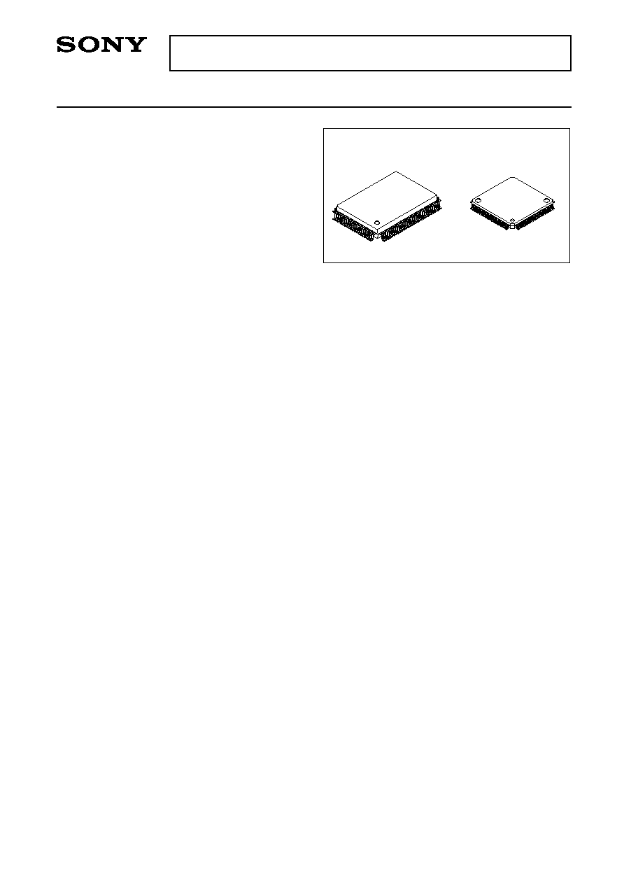
∑ Package
100-pin plastic QFP/LQFP
≠ 1 ≠
E93X30C1X-PS
Sony reserves the right to change products and specifications without prior notice. This information does not convey any license by
any implication or otherwise under any patents or other right. Application circuits shown, if any, are typical examples illustrating the
operation of the devices. Sony cannot assume responsibility for any problems arising out of the use of these circuits.
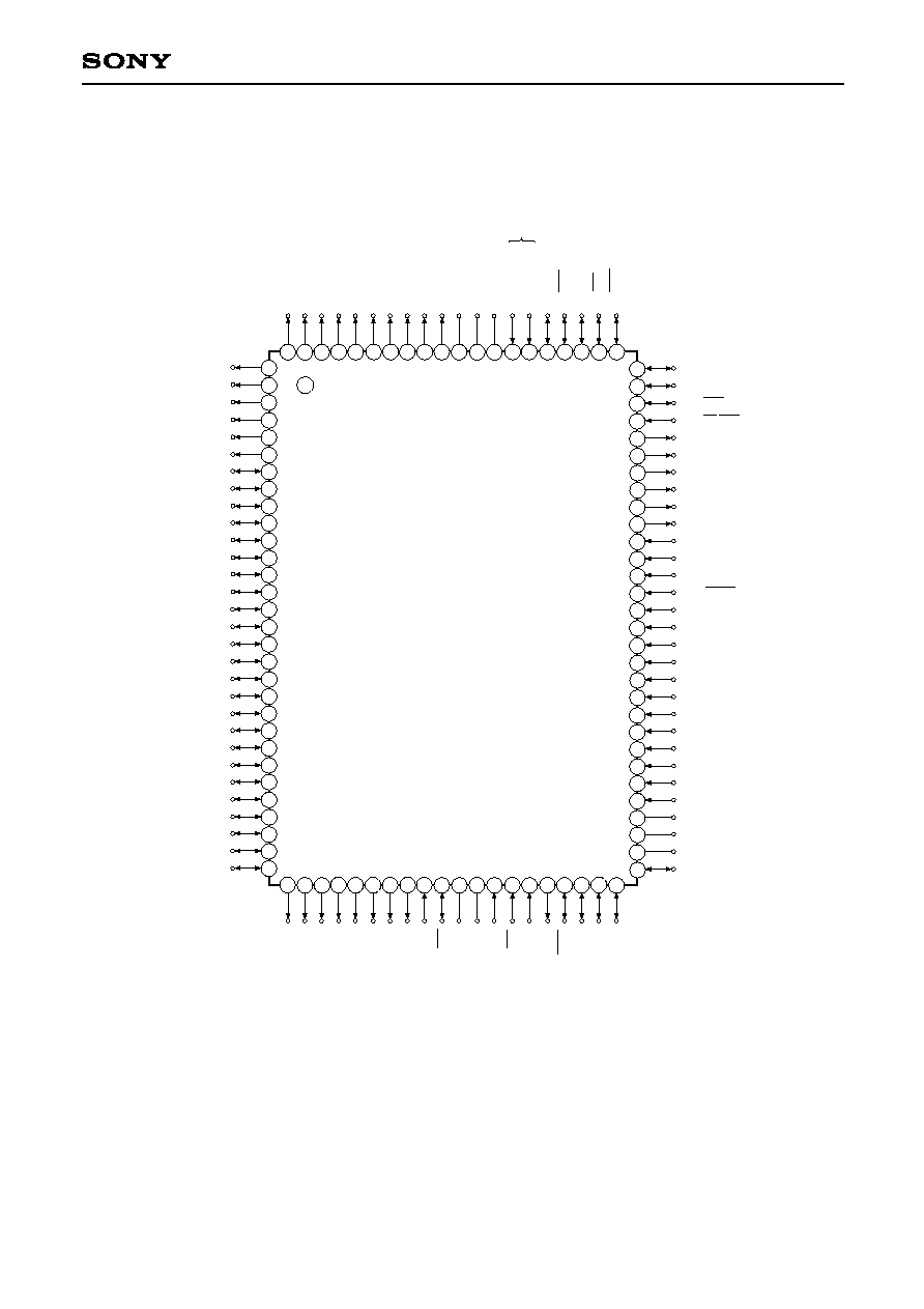
CXP871P40
100 pin QFP (PIastic)
100 pin LQFP (PIastic)
≠ 5 ≠
CXP871P40
Output/
Real time
output
Output/
Real time
output
I/O/
Real time
output
I/O/
Real time
output
I/O
Input/Input/Output
Input/Input/Input
Output/Output
Output/Output
Output/Output
Output/Output
Output/Output
Output/Output
Input
Input/Input
Output/Input
I/O
Ouput
Input
Input
(Port A)
8-bit output port. Data is gated
with PPO0 and PPO1 contents
by OR-gate and they are output.
(8 pins)
(Port B)
8-bit output port. Data is gated
with PPO0 and PPO1 contents
by OR-gate and they are output.
(8 pins)
(Port C)
8-bit I/O port. Enables to
specify I/O by bit unit.
Data is gated with PPO or
RTO contents by OR-gate
and they are output.
(8 pins)
(Port D)
8-bit I/O port. Enables to specify I/O by 4-bit unit.
Enables to drive 12mA sink current. (During 5V±0.5V operation)
(8 pins)
(Port E)
8-bit port. Lower 2 bits are
input port and upper 6 bits
are output port.
(8 pins)
Analog input pins to A/D converter. (12 pins)
(Port F)
Lower 4 bits are input port and upper 4 bits are output port.
Lower 4 bits also serve as standby release input pin.
(8 pins)
Serial clock (CH0) I/O pin.
Serial data (CH0) output pin.
Serial data (CH0) input pin.
Serial chip select (CH0) input pin.
External event
input pin for
timer/counter.
Input pin to request
external interruption.
Active when falling edge.
Input pin to request
external interruption.
Active when falling edge.
1/2 dividing
clock output of
XTAL or OSCO.
PWM output pins.
(2 pins)
DA gate pulse output pins.
(4 pins)
Programmable pattern generator
(PPG0, PPG1) output.
Functions as high precision real time
pulse output port.
(
PPG0 19 pins
)
PPG1 10 pins
Real time pulse generator (RTG)
output. Functions as high precision real
time pulse output port. (5 pins)
Symbol
I/O
Description
PA0/PPO000
/PPO100
to
PA7/PPO007
/PPO107
PB0/PPO008
to
PB7/PPO015
PC0/PPO016
to
PC2/PPO018
PC3/RTO3
to
PC7/RTO7
PD0 to PD7
PE0/INT0
/XOUT
PE1/EC/INT2
PE2/PWM0
PE3/PWM1
PE4/DAA0
PE5/DAA1
PE6/DAB0
PE7/DAB1
AN0 to AN3
PF0/AN4
to
PF3/AN7
PF4/AN8
to
PF7/AN11
SCK0
SO0
SI0
CS0
Pin Description