Description
The CXP87300 is a CMOS 8-bit single chip micro-
computer of piggyback/evaluator combined type,
which is developed for evaluating the function of the
CXP87352/87360.
Features
∑ A wide instruction set (213 instructions) which
cover various types of data.
-- 16-bit operation/multiplication and division/
boolean bit operation instructions
∑ Minimum instruction cycle
333ns at 12MHz operation (3.0 to 5.5V)
250ns at 16MHz operation (4.5 to 5.5V)
122µs at 32kHz operation
∑ Applicable EPROM
LCC type 27C256, LCC type 27C512
(Maximum 60Kbytes are available.)
∑ Incorporated RAM capacity
2048 bytes
∑ Peripheral functions
≠ A/D converter
8-bit, 12-channel, successive approximation method
(Conversion time of 20µs/16MHz)
≠ Serial interface
Incorporated buffer RAM
(Auto transfer for 1 to 32 bytes), 1 channel
Incorporated 8-bit and 8-stage FIFO
(Auto transfer for 1 to 8 bytes), 1 channel
≠ Timer
8-bit timer, 8-bit timer/counter
19-bit time base timer, 32kHz timer/counter
≠ High precision timing pattern generator
PPG 19-pin, 32-stage programmable
RTG 5 pins, 2 channels
≠ PWM/DA gate output
PWM output 12 bits, 2 channels
(Repetitive frequency 62.5kHz/16MHz)
DA gate pulse output 13 bits, 4channels
≠ Servo input control
Capstan FG, drum FG/PG, CTL input
≠ VSYNC separator
≠ FRC capture unit
Incorporated 26-bit and 8-stage FIFO
≠ PWM output
14 bits, 1 channel
≠ VISS/VASS circuit
Pulse duty auto detection circuit
≠ Remote control receiving circuit
8-bit pulse measurement counter with on-chip 6-stage FIFO
≠ General purpose prescaler
7 bits (SYNC1 input frequency division, FRC capture possible.)
≠ HSYNC counter
12-bit event counter (SYNC1 input count)
∑ Interruption
22 factors, 15 vectors, multi-interruption possible
∑ Standby mode
SLEEP/STOP
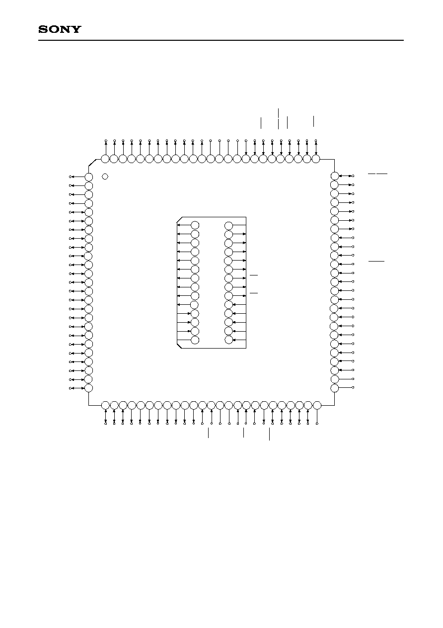
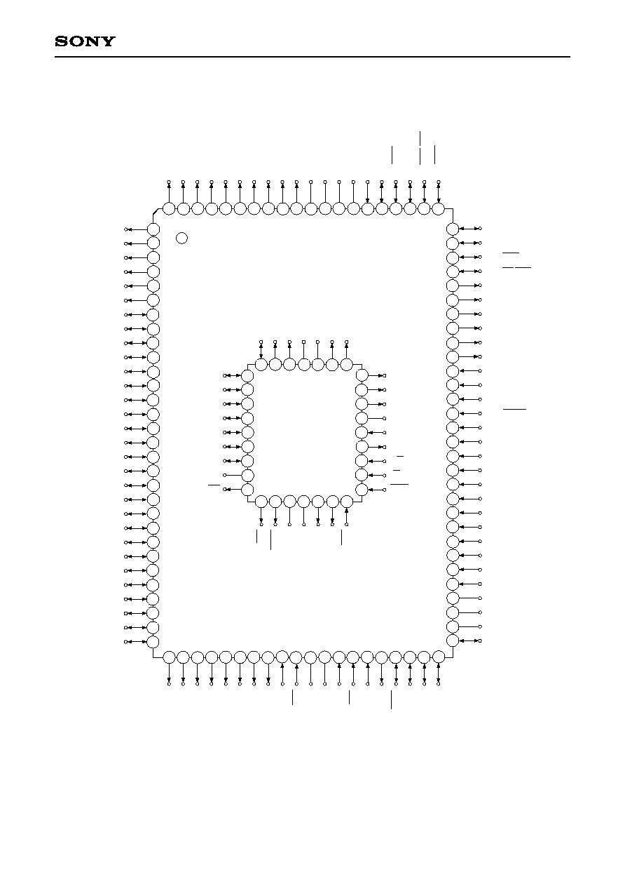
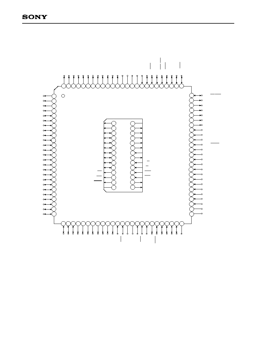
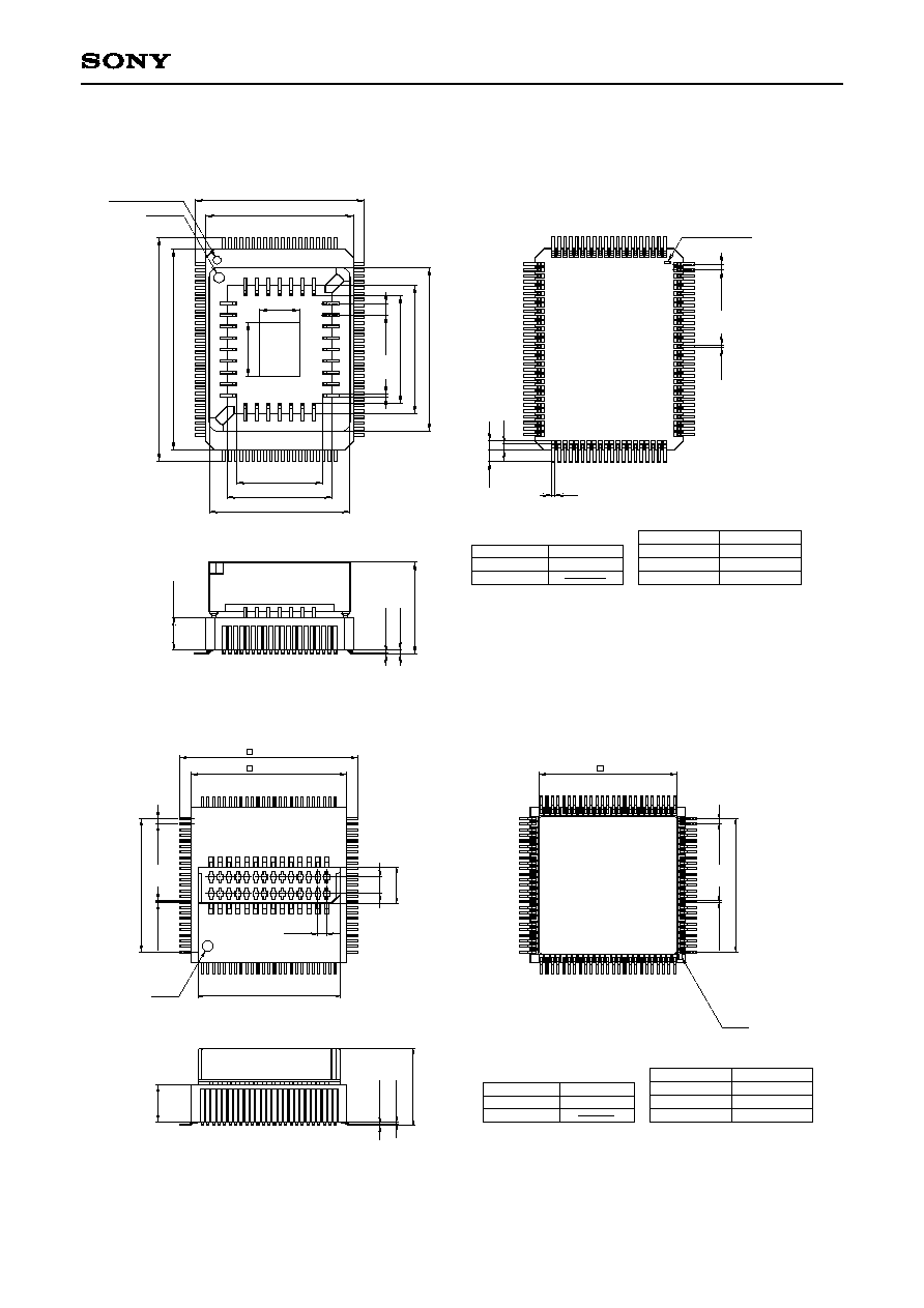
∑ Package
100-pin ceramic PQFP
Note) Mask option depends on the type of the CXP87300. Refer to the Products List for details.
Structure
Silicon gate CMOS IC
≠ 1 ≠
CXP87300
E94X15A68-PS
CMOS 8-bit Single Chip Microcomputer
Sony reserves the right to change products and specifications without prior notice. This information does not convey any license by
any implication or otherwise under any patents or other right. Application circuits shown, if any, are typical examples illustrating the
operation of the devices. Sony cannot assume responsibility for any problems arising out of the use of these circuits.
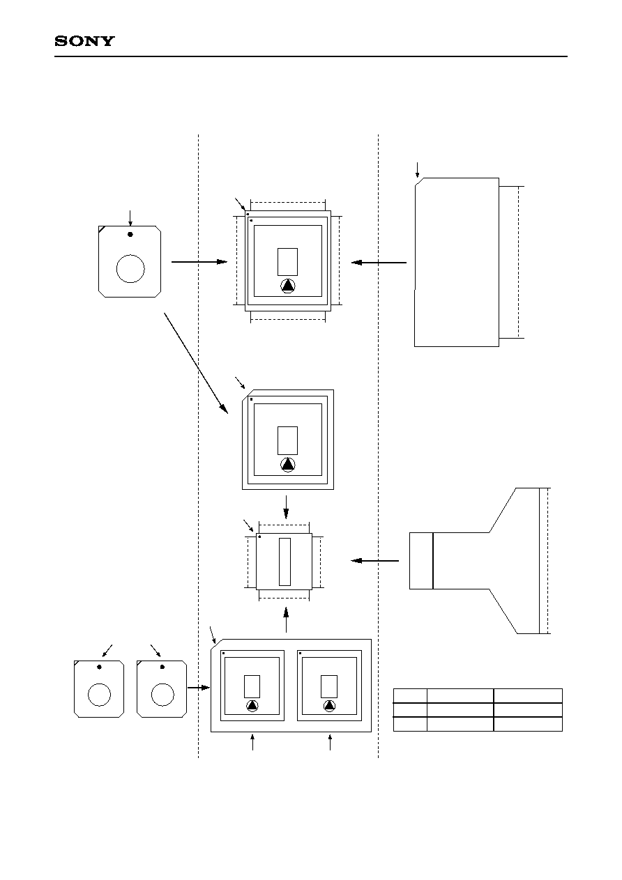
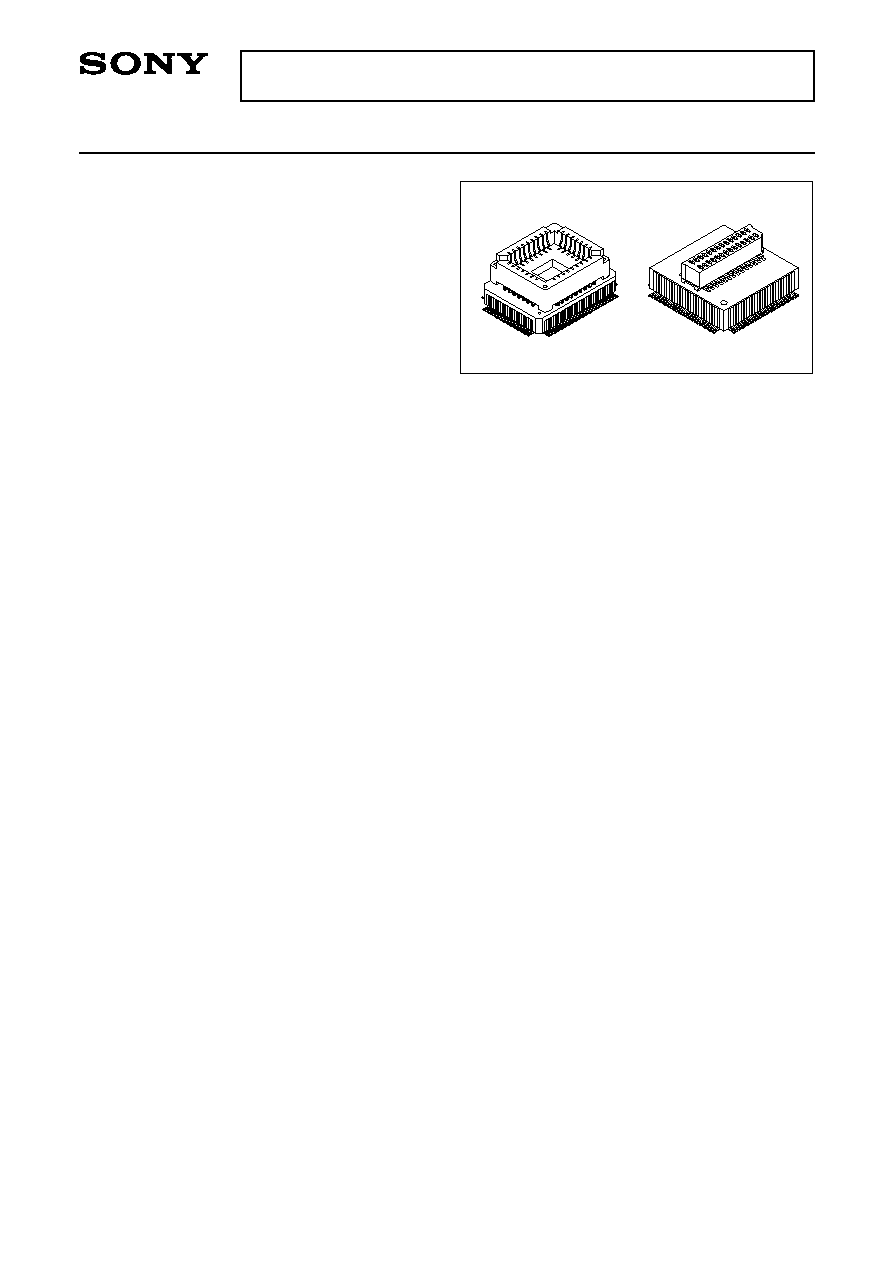
Piggyback/
evaluator type
100 pin PQFP (Ceramic)
QFP supported
LQFP supported

≠ 6 ≠
CXP87300
EPROM Read Timing (Ta = ≠20 to +75∞C, V
DD
= 3.0 to 5.5V, Vss = 0V)
Address
data
hold time
Address
data
input delay time
Item
Symbol
Pin
Min.
Max.
Unit
t
IH
t
ACC
A0 to A15
D0 to D7
A0 to A15
D0 to D7
0
100
1
75
2
ns
ns
t
ACC
t
IH
0.8V
DD
0.8V
DD
0.2V
DD
0.2V
DD
Input data
Address data
A0 to A15
D0 to D7
Products
Option item
TTL schmitt
Existent
CMOS schmitt
27C512
◊
1
27C512
◊
1
1
On PG4/SYNC0 pin and PG5/SYNC1 pin, the input circuit format can be selected to every pin.
Products List
1
At 12MHz operation (V
DD
= 4.5 to 5.5V)
2
At 12MHz operation (V
DD
= 3.0 to 5.5V), At 16MHz operation (V
DD
= 4.5 to 5.5V)
Piggyback/evaluator product
CXP87300-U01Q
CXP87300-U01R
100-pin ceramic
PQFP
EPROM 60Kbytes
27C256
◊
2
Mask product
100-pin plastic
QFP/LQFP
Existent/Non-existent
CMOS schmitt/TTL schmitt
52Kbytes
60Kbytes
CXP87360
CXP87352
CMOS schmitt
CXP87300-U02Q
CXP87300-U02R
CXP87300-U05R
Package
ROM capacity
Pull-up resistor
for reset pin
Input circuit format
1