Description
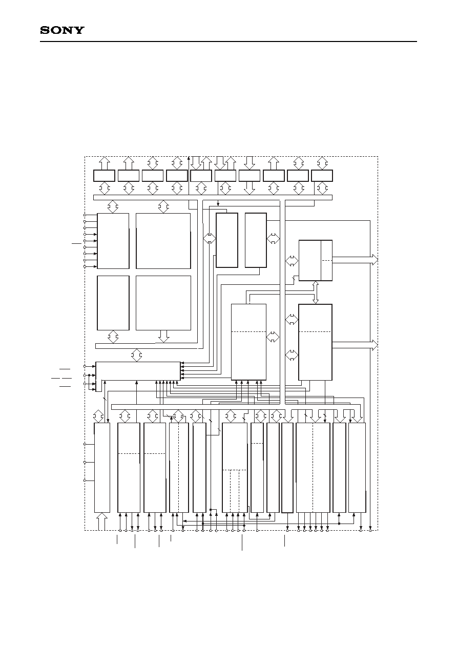
The CXP873P60 is a CMOS 8-bit micro-computer
which consists of A/D converter, serial interface,
timer/counter, time base timer, vector interruption,
high precision timing pattern generation circuit, PWM
generator, PWM for tuner, VISS/VASS circuit, 32kHz
timer/event counter, remote control receiving circuit,
general purpose prescaler, HSYNC counter, VCR
vertical sync separation circuit and the measurement
circuit which measure signals of capstan FG and
drum FG/PG and other servo systems, as well as
basic configurations like 8-bit CPU, PROM, RAM and
I/O port. They are integrated into a single chip.
Also the CXP873P60 provides sleep/stop function
which enables to lower power consumption and ultra-
low speed instruction mode in 32kHz operation.
Incorporating a one-time PROM, the CXP873P60
has an equivalent function to the CXP87360, and is
suitable for evaluation in system development and for
the production of small amounts.
Features
· A wide instruction set (213 instructions) which cover various types of data
-- 16-bit arithmetic/multiplication and division/boolean bit operation instructions
· Minimum instruction cycle
250ns at 16MHz operation (4.5V to 5.5V)
333ns at 12MHz operation (3.0V to 5.5V)
122µs at 32kHz operation
· Incorporated PROM capacity
60K bytes
· Incorporated RAM capacity
2048 bytes
· Peripheral functions
-- A/D converter
8-bit, 12-channel, successive approximation system
(Conversion time 20.0µs/16MHz)
-- Serial interface
Incorporated buffer RAM (1 to 32 bytes auto transfer) 1-channel
Incorporated 8-bit and 8-stage FIFO for data
(1 to 8 bytes auto transfer) 1-channel
-- Timer
8-bit timer, 8-bit timer/counter, 19-bit time base timer,
32kHz timer/counter
-- High precision timing pattern generator
PPG 19-pin 32-stage programmable
RTG 5-pin 2-channel
-- PWM/DA gate output
PWM 12-bit, 2-channel (Repetitive frequency 62kHz/16MHz)
DA gate pulse output 13-bit, 4-channel
-- Servo input control
Capstan FG, Drum FG/PG, CTL input
-- VSYNC separator
-- FRC capture unit
Incorporated 26-bit and 8-stage FIFO
-- PWM output
14-bit, 1-channel
-- VISS/VASS circuit
Pulse duty auto detection circuit
-- Remote control receiving circuit
8-bit pulse measurement counter with on-chip, 6-stage FIFO
-- General purpose prescaler
7-bit (SYNC1 input frequency divided, FRC capture possible)
-- HSYNC counter
12-bit event counter (Counts SYNC1 input.)
· Interruption
21 factors, 15 vectors, multi-interruption possible
· Standby mode
SLEEP/STOP
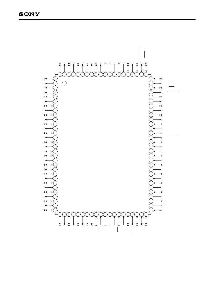
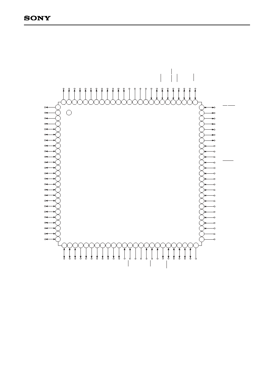
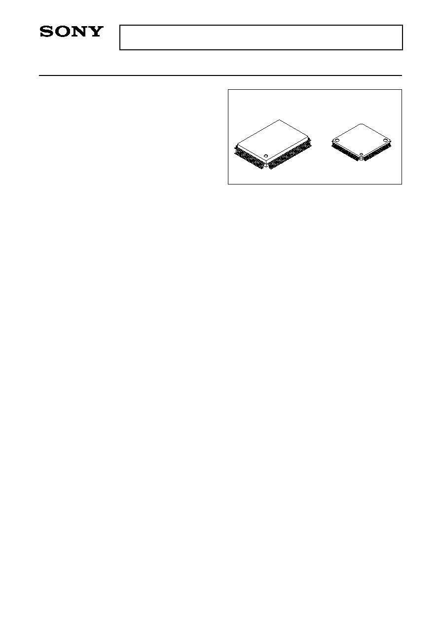
· Package
100-pin plastic QFP/LQFP
1
CXP873P60
E95106A31
CMOS 8-bit Single Chip Microcomputer
Sony reserves the right to change products and specifications without prior notice. This information does not convey any license by
any implication or otherwise under any patents or other right. Application circuits shown, if any, are typical examples illustrating the
operation of the devices. Sony cannot assume responsibility for any problems arising out of the use of these circuits.
100 pin QFP (PIastic)
100 pin LQFP (PIastic)
Structure
Silicon gate CMOS IC
5
CXP873P60
Output/
Real time
output
Output/
Real time
output
I/O/
Real time
output
I/O/
Real time
output
I/O
Input/Input/Output
Input/Input/Input/
Output
Output/Output
Output/Output
Output/Output
Output/Output
Output/Output
Output/Output
Input
Input/Input
Output/Input
I/O
Ouput
Input
Input
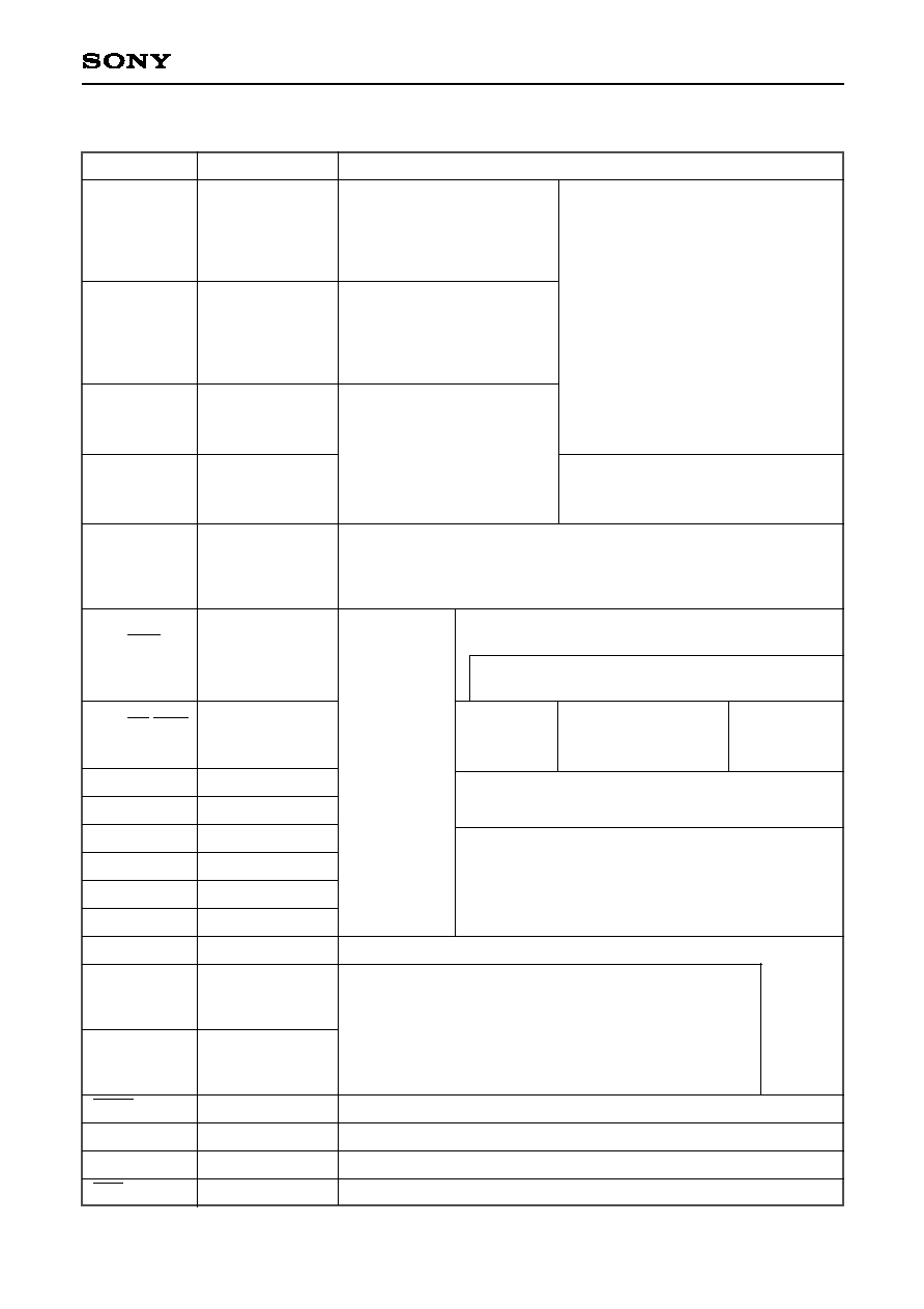
(Port A)
8-bit output port. Data is
gated with PPO contents by
OR-gate and they are output.
(8 pins)
(Port B)
8-bit output port. Data is
gated with PPO contents by
OR-gate and they are output.
(8 pins)
(Port C)
8-bit I/O port, enables to
specify I/O by bit unit.
Data is gated with PPO or
RTO contents by OR-gate
and they are output.
(8 pins)
(Port D)
8-bit I/O port. Enable to specify I/O by 4-bit unit.
Enables to drive 12mA sink current.
(8 pins)
(Port E)
8-bit port.
Lower 2 bits
are input pins
and upper 6
bits are output
pins.
(8 pins)
Analog input pins to A/D converter. (12 pins)
(Port F)
Lower 4 bits are input port and upper 4 bits are output port.
Lower 4 bits also serve as standby release input pin.
(8 pins)
Serial clock (CH0) I/O pin.
Serial data (CH0) output pin.
Serial data (CH0) input pin.
Serial chip select (CH0) input pin.
External event
input pin for
timer/counter.
Input pin to request
external interruption.
Active when falling edge.
Input pin to request external interruption.
Active when falling edge.
PC3 can be 3-state controlled with RTG.
System clock frequency division output.
PWM output pins.
(2 pins)
DA gate pulse output pins.
(4 pins)
Programmable pattern generator (PPG)
output.
Functions as high precision real time
pulse output port.
(19 pins)
PB0 and PB2 can be 3-state controlled
with PPG.
Real time pulse generator (RTG) output.
Functions as high precision real time
pulse output port. (5 pins)
Symbol
I/O
Description
PA0/PPO0
to
PA7/PPO7
PB0/PPO8
to
PB7/PPO15
PC0/PPO16
to
PC2/PPO18
PC3/RTO3
to
PC7/RTO7
PD0 to PD7
PE0/INT0/
CKOUT
PE1/EC/INT2/
HCOUT
PE2/PWM0
PE3/PWM1
PE4/DAA0
PE5/DAA1
PE6/DAB0
PE7/DAB1
AN0 to AN3
PF0/AN4
to
PF3/AN7
PF4/AN8
to
PF7/AN11
SCK0
SO0
SI0
CS0
Pin Description
Coinsidence
signal output of
HSYNC counter.