 | –≠–ª–µ–∫—Ç—Ä–æ–Ω–Ω—ã–π –∫–æ–º–ø–æ–Ω–µ–Ω—Ç: CXP875P40 | –°–∫–∞—á–∞—Ç—å:  PDF PDF  ZIP ZIP |
Description
The CXP875P40 is a CMOS 8-bit micro-computer
which consists of arithmetic coprocessor, A/D
converter, serial interface, timer/counter, time base
timer, vector interruption, high precision timing
pattern generation circuit, PWM generator and the
measuring circuit which measure signals of capstan
FG, drum FG/PG, reel FG and other servo systems,
as well as basic configurations like 8-bit CPU,
PROM, RAM and I/O port. They are integrated into a
single chip.
Also this IC provides power on reset function,
sleep/stop function which enables to lower power
consumption.
The CXP875P40 is the one-chip PROM version of
the CXP87532/87540 with mask ROM, providing the
function of being able to write directly into the
program. It is suitable for evaluation use during
system development and for small quantity
production.
Features
∑ A wide instruction set (213 instructions) which cover various types of data
-- 16-bit operation code/multiplying instruction/boolean bit operation instruction
∑ Minimum instruction cycle
During operation 326ns/12.288MHz
∑ Incorporated PROM capacity
40K bytes
∑ Incorporated RAM capacity
1344 bytes
∑ Peripheral functions
-- Arithmetic coprocessor
Multiplying with code, sum of products with code, high speed
execution of many bits shift rotation operation
-- A/D converter
8-bit, 8-channel, successive approximation system
(Conversion time 13µs/12.288MHz)
Incorporated 3-stage FIFO for A/D conversion data
-- Serial interface
Incorporated buffer RAM for data
(1 to 128 bytes auto transfer) 2-channel
-- Timer
8-bit timer, 8-bit timer/counter, 19-bit time base timer
-- High precision timing pattern generator
PPG (11 pins) 32-stage programmable
-- PWM output
12-bit, 2-channel (Repeated frequency 48kHz)
8-bit, 3-channel (Repeated frequency 48kHz)
-- Servo input control
Capstan FG, Drum FG/PG, Reel FG input
-- FRC capture unit
Incorporated 28-bit and 8-stage FIFO
∑ Interruption
12 factors, 12 vectors, multi-interruption possible
∑ Standby mode
SLEEP/STOP
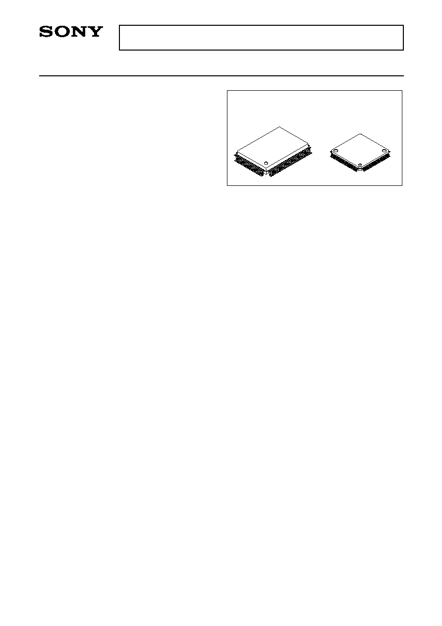
∑ Package
100-pin plastic QFP/LQFP
Structure
Silicon gate CMOS IC
≠ 1 ≠
CXP875P40
E94317-PS
CMOS 8-bit Single Chip Microcomputer
Sony reserves the right to change products and specifications without prior notice. This information does not convey any license by
any implication or otherwise under any patents or other right. Application circuits shown, if any, are typical examples illustrating the
operation of the devices. Sony cannot assume responsibility for any problems arising out of the use of these circuits.
100 pin QFP (Plastic)
100 pin LQFP (Plastic)
≠ 2 ≠
CXP875P40
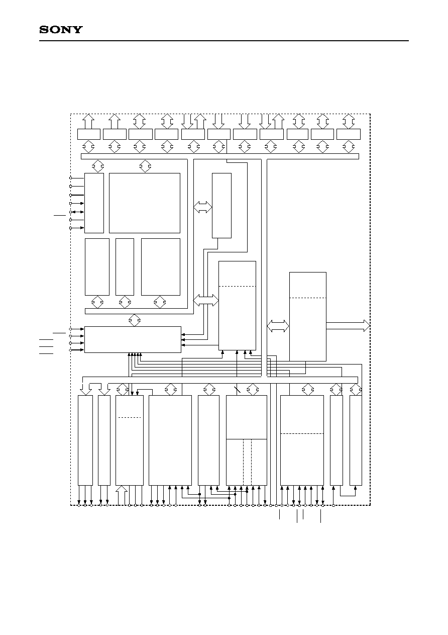
6
SPC700
CPU CORE
CO-PROCESSOR
PROM
40K BYTES
CLOCK GENERATOR/
SYSTEM CONTROL
RAM
1120 BYTES
PRESCALER/
TIME BASE TIMER
FRC
CAPTURE
UNIT
FIFO
INTERRUPT CONTROLLER
8BIT PWM GENERATOR 3CH
12BIT PWM GENERATOR 2CH
ATF SYNC UNIT
SWITCHING PULSE
GENRATOR
8BIT TIMER/COUNTER 0
8BIT TIMER 1
A/D CONVERTER
FIFO
SERVO
INPUT
CONTROL
DRUM
CAPSTAN
REEL
SERIAL
INTERFACE
UNIT
RAM
NM1
PE1/INT2
PE3/INT1
PE0/INT0
PE2/PWM0
PE3/PWM1
PE4/PWM2
PE5/PWM3
PE6/PWM4
PF0/AN0 to PF7/AN7
AV
DD
AV
REF
AV
SS
PA4/ATFS1
PA5/ATFS3
PA7/ATFS2
PK0/RFDT
PK1/MCLK
PE7/SWP
PA6/AREA
PG2/DREF
PG3/DPG
PG4/DFG
PG5/CFG
PG6/RFG0
PG7/RFG1
PA3/PROUT
PG0/EXI0
PG1/EXI1
SI0
SO0
PH2/SI1
PH1/SO1
PE1/EC
PB0/PPO0
to
PA2/PPO10
8
CS0
SCK0
PH3/CS1
PH0/SCK1
PA0 to PA7
PORT A
PB0 to PB7
PORT B
PC0 to PC7
PORT C
PD0 to PD7
PORT D
PE0 to PE1
PE2 to PE7
PORT E
PF0 to PF7
PORT F
PG0 to PG7
PORT G
PH0 to PH3
PH4 to PH7
PORT H
PI0 to PI7
PORT I
PK0 to PK3
PORT K
PJ0 to PJ7
PORT J
PROGRAMMABLE
PATTERN
GENERATOR
RAM
V
SS
V
DD
MP
XTAL
EXTAL
RST
V
PP
Block Diagram
≠ 3 ≠
CXP875P40
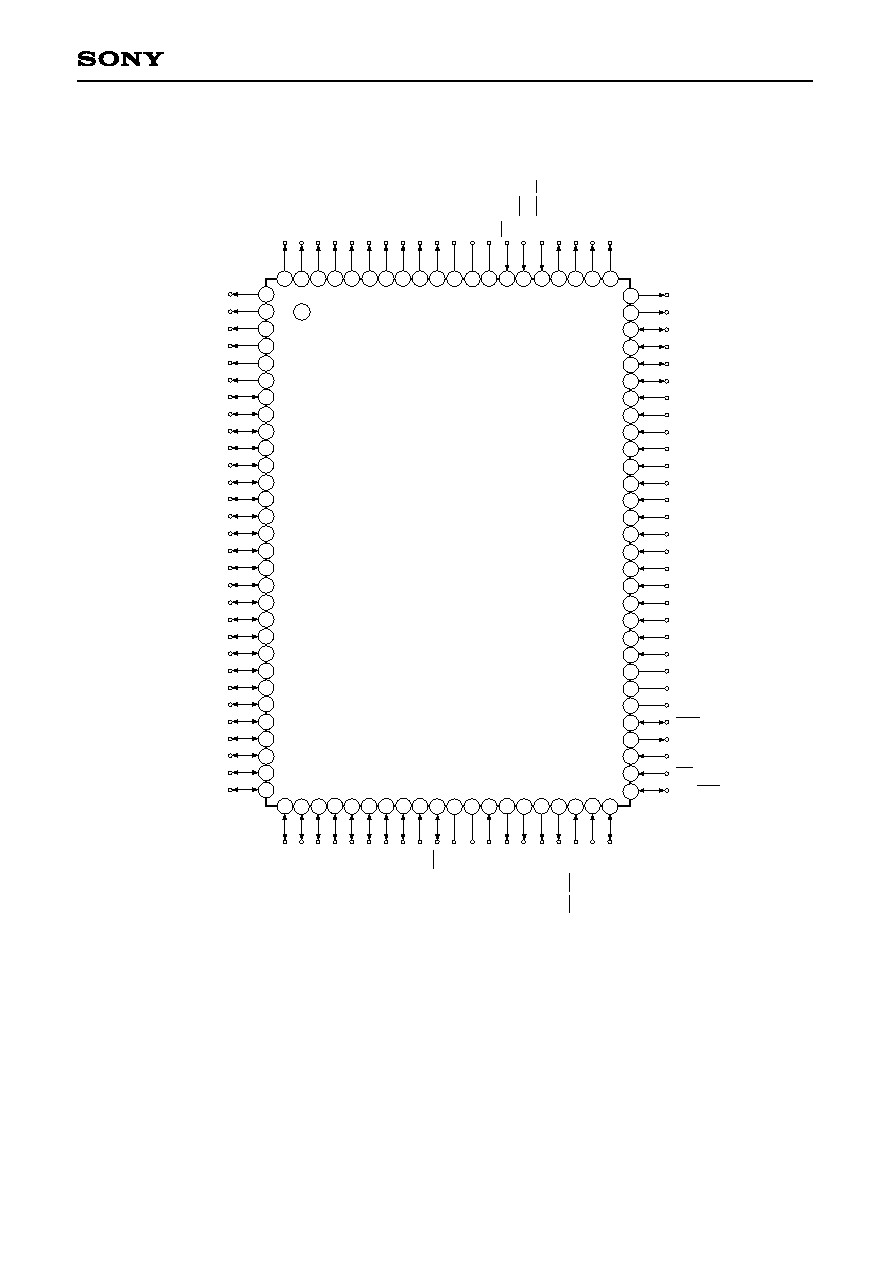
Pin Configuration 1 (Top View) 100pin QFP
2
3
4
5
6
7
8
9
10
11
12
13
14
15
16
17
18
19
20
21
22
23
24
25
26
27
28
29
30
40
39
38
37
36
35
34
31 32 33
41 42 43 44 45 46 47 48 49 50
51
52
53
54
55
56
57
58
59
60
70
69
68
67
63
64
65
66
61
62
71
72
73
74
81
82
83
84
75
76
77
78
88 87 86 85
79
89
90
100 99 98 97 96 95 94
91
92
93
1
80
PE6/PWM4
PE7/SWP
PK0/RFDT
PK1/MCLK
PK2
PK3
PG0/EXI0
PG1/EXI1
PG2/DREF
PG3/DPG
PG4/DFG
PG5/CFG
PG6/RFG0
PG7/RFG1
PF0/AN0
PF1/AN1
PF2/AN2
PF3/AN3
PF4/AN4
PF5/AN5
PF6/AN6
PF7/AN7
AV
DD
AV
REF
AV
SS
SCK0
SO0
SI0
CS0
PH0/SCK1
PPO5/PB5
PPO4/PB4
PPO3/PB3
PPO2/PB2
PPO1/PB1
PPO0/PB0
PC7
PC6
PC5
PC4
PC3
PC2
PC1
PC0
PD7
PD6
PD5
PD4
PD3
PD2
PD1
PD0
PI7
PI6
PI5
PI4
PI3
PI2
PI1
PI0
PB6/PPO6
PB7/PPO7
PA0/PPO8
PA1/PPO9
PA2/PPO10
PA3/PROUT
PA4/ATFS1
PA5/ATFS3
PA6/AREA
PA7/ATFS2
V
PP
V
DD
V
SS
NMI
PE0/INT0
PE1/INT2/EC
PE2/PWM0
PE3/PWM1
PE4/PWM2
PE5/PWM3
PJ7
PJ6
PJ5
PJ4
PJ3
PJ2
PJ1
PJ0
MP
RST
V
SS
XTAL
EXTAL
PH7
PH6
PH5
PH4
CS1/INT1/PH3
SI1/PH2
SO1/PH1
Note) 1. V
PP
(Pin 90) is always connected to V
DD
.
2. V
SS
(Pins 41 and 88) are both connected to GND.
3. MP (Pin 39) is always connected to V
SS
.

≠ 4 ≠
CXP875P40
Pin Configuration 2 (Top View) 100pin LQFP
2
3
4
5
6
7
8
9
10
11
12
13
14
15
16
17
18
19
20
21
22
23
24
25
40
39
38
37
36
35
34
31 32 33
41 42 43 44 45 46 47 48 49 50
51
52
53
54
55
56
57
58
59
60
70
69
68
67
63
64
65
66
61
62
71
72
73
74
81
82
83
84
75
76
77
78
88 87 86 85
79
89
90
100 99 98 97 96 95 94
91
92
93
1
80
PE6/PWM4
PE7/SWP
PK0/RFDT
PK1/MCLK
PK2
PK3
PG0/EXI0
PG1/EXI1
PG2/DREF
PG3/DPG
PG4/DFG
PG5/CFG
PG6/RFG0
PG7/RFG1
PF0/AN0
PF1/AN1
PF2/AN2
PF3/AN3
PF4/AN4
PF5/AN5
PF6/AN6
PF7/AN7
AV
DD
AV
REF
AV
SS
PBO3/PB3
PPO2/PB2
PPO1/PB1
PPO0/PB0
PC7
PC6
PC5
PC4
PC3
PC2
PC1
PC0
PD7
PD6
PD5
PD4
PD3
PD2
PD1
PD0
PI7
PI6
PI5
PB6/PPO6
PB7/PPO7
PA0/PPO8
PA1/PPO9
PA2/PPO10
PA3/PROUT
PA4/ATFS1
PA5/ATFS3
PA6/AREA
PA7/ATFS2
V
PP
V
DD
V
SS
NMI
PE0/INT0
PE1/EC/INT2
PE2/PWM0
PE3/PWM1
PE4/PWM2
PE5/PWM3
PJ2
PJ1
PJ0
MP
RST
V
SS
XTAL
EXTAL
PH7
PH6
PH5
PH4
CS1/INT1/PH3
SI1/PH2
SO1/PH1
PJ7
PJ6
PJ5
PJ4
PJ3
26 27 28 29 30
PI4
PI3
PI2
PI1
PI0
SCK1/PH0
CS0
SCK0
SO0
SI0
PB4/PPO4
PB5/PPO5
Note) 1. V
PP
(Pin 88) is always connected to V
DD
.
2. V
SS
(Pins 39 and 86) are both connected to GND.
3. MP (Pin 37) is always connected to V
SS
.
≠ 5 ≠
CXP875P40
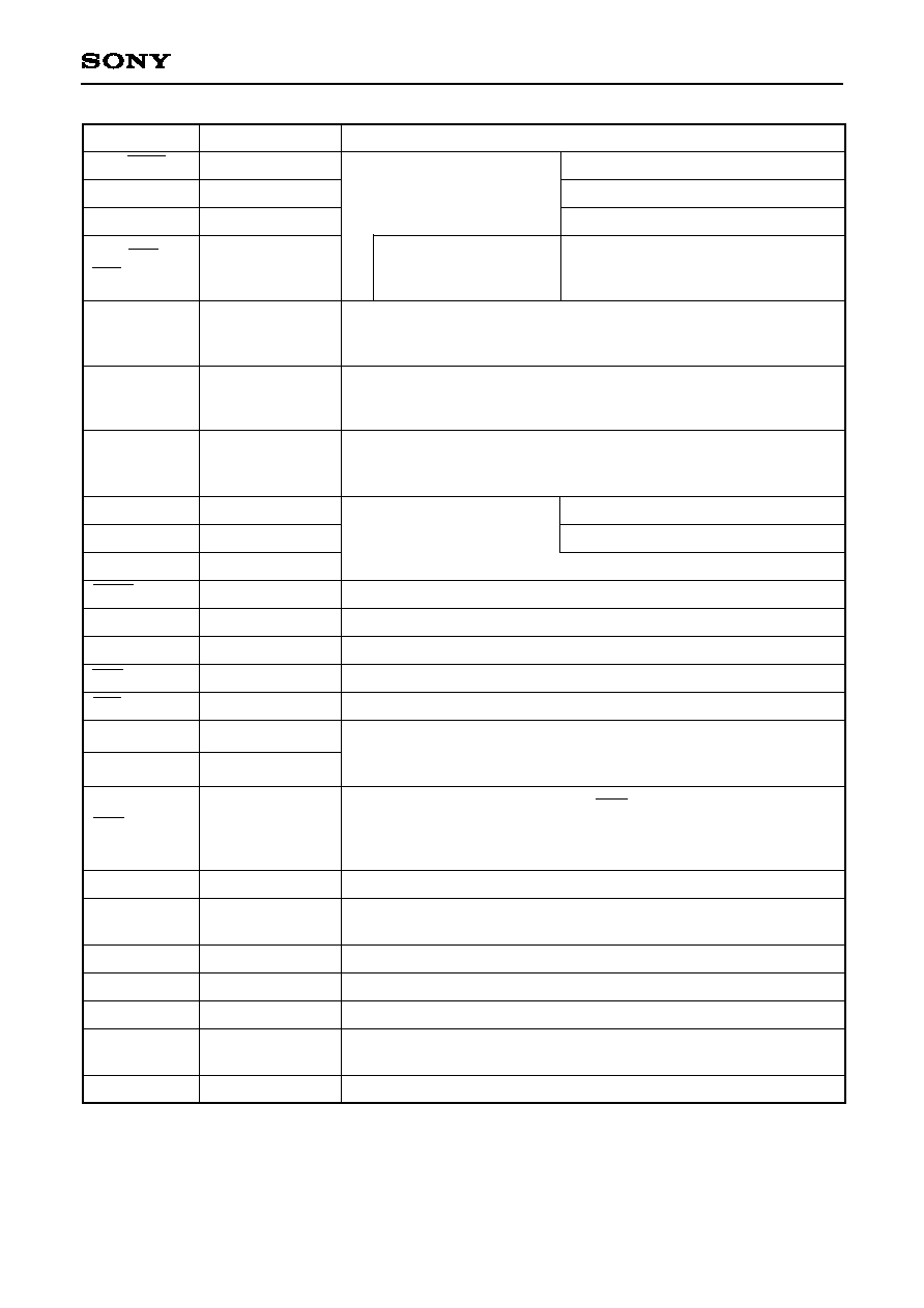
(Port C)
8-bit input/output port, enables to specify input/output by 4-bit unit.
(8 pins)
Output/
Real time output
Output/
Monitor output
Output/
Real time output
I/O
I/O
Input/Input
Input/Input/
Input
Output/Output
Output/Output
Input/Input
Input/Input
Input/Input
Input/Input
Input/Input
Input/Input
Input/Input
Input/Input
Input/Input
(Port B)
8-bit output port. Data is gated
with PPO by OR-gate and
they are output. (8 pins)
(Port D)
8-bit input/output port. Lower 4 bits can be specified as input/output by
bit unit and upper 4 bits can be specified as input/output by 4-bit unit.
(8 pins)
(Port E)
8-bit port. Lower 2 bits
are input pins and upper
6 bits are output pins.
(8 pins)
External input pin 0.
External input pin 1.
Drum reference signal input pin.
Drum PG input pin.
Drum FG input pin.
Capstan FG input pin.
Reel FG input pin.
Input pin to request external interruption.
Active when falling edge.
PWM output pins (5 pins)
SWP output pin.
Programmable pattern generator (PPG)
Output (3 pins) and capstan servo control
signal (1 pin).
Symbol
I/O
Description
PA0/PPO8
PA1/PPO9
PA2/PPO10
PA3/PROUT
PA4/ATFS1
PA5/ATFS3
PA6/AREA
PA7/ATFS2
PB0/PPO0
to
PB7/PPO7
PC0 to PC7
PD0 to PD7
PE0/INT0
PE1/EC/INT2
PE2/PWM0
to
PE6/PWM4
PE7/SWP
PF0/AN0
to
PF7/AN7
PG0/EXI0
PG1/EXI1
PG2/DREF
PG3/DPG
PG4/DFG
PG5/CFG
PG6/RFG0
PG7/RFG1
(Port A)
8-bit output port.
Data is gated with PPO
(3 pins), monitor signal
(4 pins) in relation to ATF,
control signal (1 pin) for
capstan servo by OR-gate
and they are output. (8 pins)
Monitor output in relation to ATF.
(4 pins)
Programmable pattern generator (PPG)
output. (8 pins)
External event
input pin for
timer/counter.
(Port F)
8-bit input port. (8 pins)
Upper 4 bits serve as
standby release input pin.
(Port G)
8-bit input port.
(8 pins)
Analog input pins to A/D converter.
(8 pins)
Pin Description
Input pin to request external
interruption. Active when
falling edge.
≠ 6 ≠
CXP875P40
Symbol
I/O
Description
PH0/SCK1
PH1/SO1
PH2/SI1
PH3/INT1/
CS1
PH7 to PH4
PI0 to PI7
PJ0 to PJ7
PK0/RFDT
PK1/MCLK
PK2 to PK3
SCK0
SO0
SI0
CS0
NMI
EXTAL
XTAL
RST
MP
AV
DD
AV
REF
AV
SS
V
DD
V
PP
V
SS
Input/I/O
Input/Output
Input/Input
Input/Input/Input
Output
I/O
I/O
I/O/Input
I/O/Input
I/O
I/O
Output
Input
Input
Input
Input
Output
I/O
Input
Input
Serial clock input/output pin.
Serial data output pin.
Serial data input pin.
Chip select input pin to serial interface.
Serial clock input/output pin.
Serial data output pin.
Serial data input pin.
Chip select input pin to serial interface.
Non-maskable interrupt request pin. Active during falling edge.
Connecting pin of crystal oscillator for system clock. When supplying
the external clock, input the external clock to EXTAL pin and set XTAL
pin to open.
System reset pin of active "L" level. RST pin is input/output pin, which
output "L" level by incorporated power on reset function when power
ON. (Mask option)
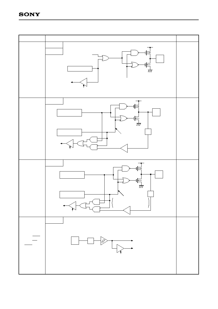
(Port H)
4-bit input port.
(4 pins)
Input pin to request
external interruption.
Active when falling edge.
(Port H)
4-bit output port. N-ch open drain output of middle tension proof (12V)
and high current (12mA). (4 pins)
(Port I)
8-bit input/output port, enables to specify input/output by 4-bit unit.
(8 pins)
(Port J)
8-bit input/output port, enables to specify input/output by 4-bit unit.
(8 pins)
(Port K)
4-bit input/output port,
enables to specify input/
output by bit unit. (4 pins)
Playback data input pin.
Channel clock input pin.
Test mode pin. This pin is always connected to GND.
Positive power supply pin of A/D converter.
Set the same voltage as V
DD
.
Reference voltage input pin of A/D converter.
GND pin of A/D converter.
Positive power supply pin.
Positive power supply pin for incorporated PROM writing.
In normal operation, connect to V
DD
.
GND pin. Connect both V
SS
pins to GND.
≠ 7 ≠
CXP875P40
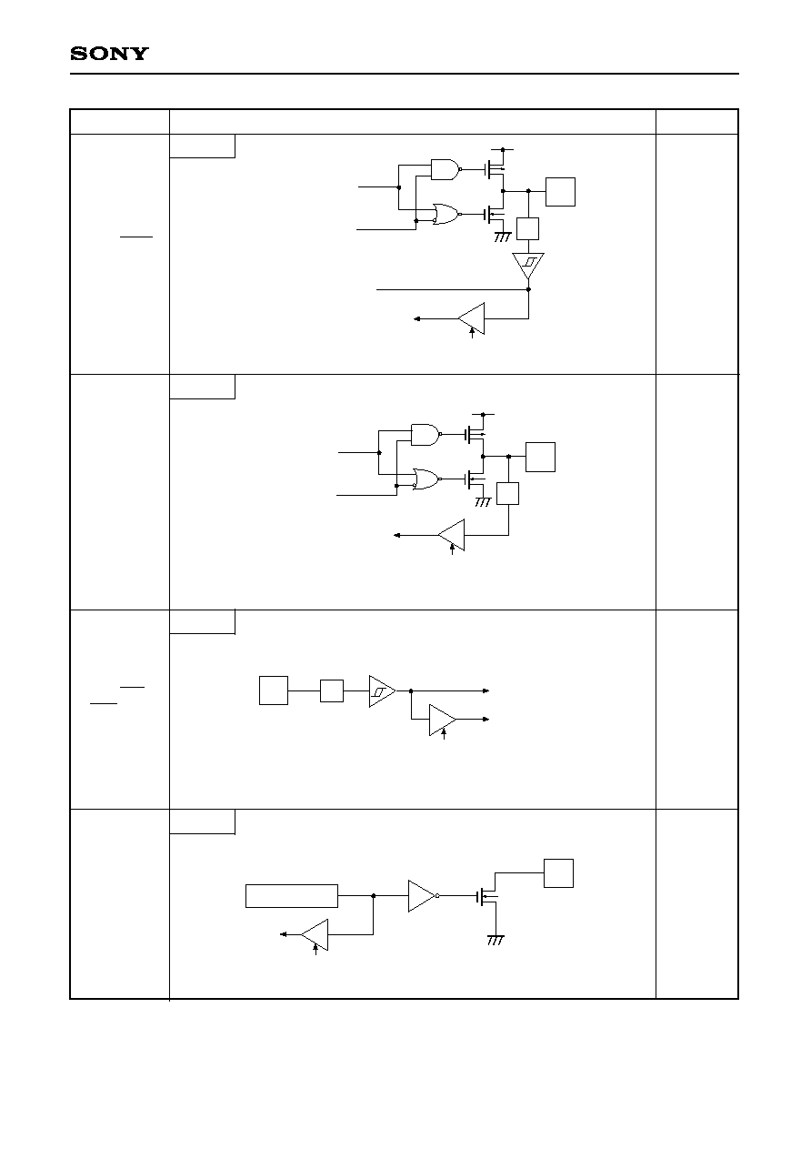
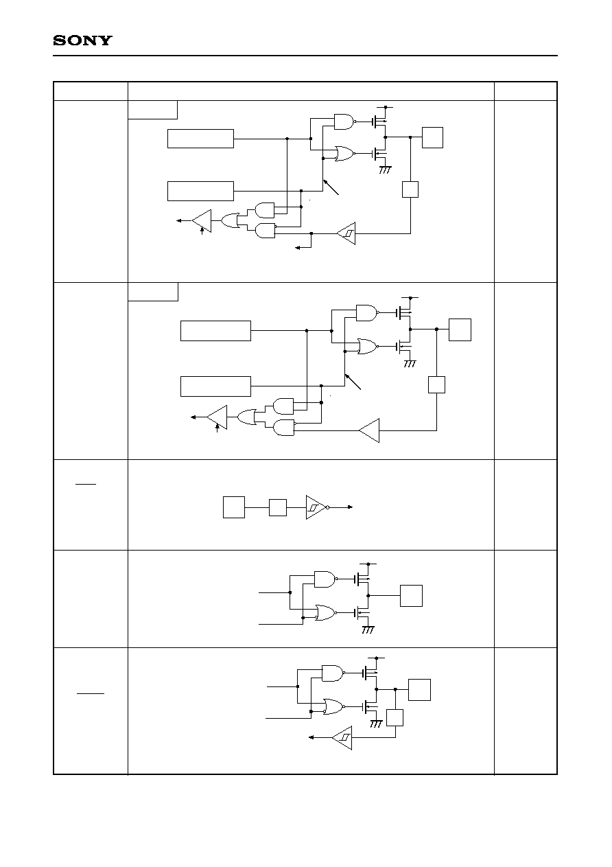
I/O Circuit Formats for Pins
Pin
Circuit format
When reset
Port A
Port B
Port C
Port D
Port E
Hi-Z
Hi-Z
Hi-Z
Hi-Z
PA0/PPO8
to
PA2/PPO10
PA3/PROUT
PA4/ATFS1
PA5/ATFS3
PA6/AREA
PA7/ATFS2
PB0/PPO0
to
PB7/PPO7
16 pins
PC0
to
PC7
8 pins
PD0
to
PD7
8 pins
PE0/INT0
PE1/EC/
INT2
2 pins
PPO, PROUT,
ATFS1 to ATFS3,
AREA, data
Data bus
Output becomes active from high impedance
by data writing to port register.
Port A or Port B
RD
Data bus
RD (Port D)
Port D direction
Port D data
IP
Large current
12mA
Lower 4 bits are by bit unit
and upper 4 bits are by 4-
bit unit
Data bus
RD (Port C)
Port C direction
Port C data
IP
Input protection
circuit
(Every 4 bits)
Buffer
IP
RD (Port E)
Data bus
Schmitt input
≠ 8 ≠
CXP875P40
Port E
Port E
Port F
Port G
Hi-Z
H level
Hi-Z
Hi-Z
PE2/PWM0
PE3/PWM1
PE4/PWM2
PE5/PWM3
4 pins
PE6/PWM4
PE7/SWP
2 pins
PF0/AN0
to
PF7/AN7
8 pins
PG0/EXI0
PG1/EXI1
PG2/DREF
PG3/DPG
PG4/DFG
PG5/CFG
PG6/RFG0
PG7/RFG1
8 pins
Data bus
RD (Port E)
PWM output
MPX
Port/PWM output
select
Port E data
Hi-Z control
Data bus
RD (Port E)
Port/PWM, SWP
output select
PWM, SWP output
MPX
Port E data
IP
Input multiplexer
A/D converter
Analog/Digial
tinput select
RD (Port F)
Data bus
IP
RD (Port G)
Data bus
Schmitt input
Servo input
For PG0/EXI0 to PG7/RFG1, TTL schmitt input can be
selected with the mask option.
Pin
Circuit format
When reset
≠ 9 ≠
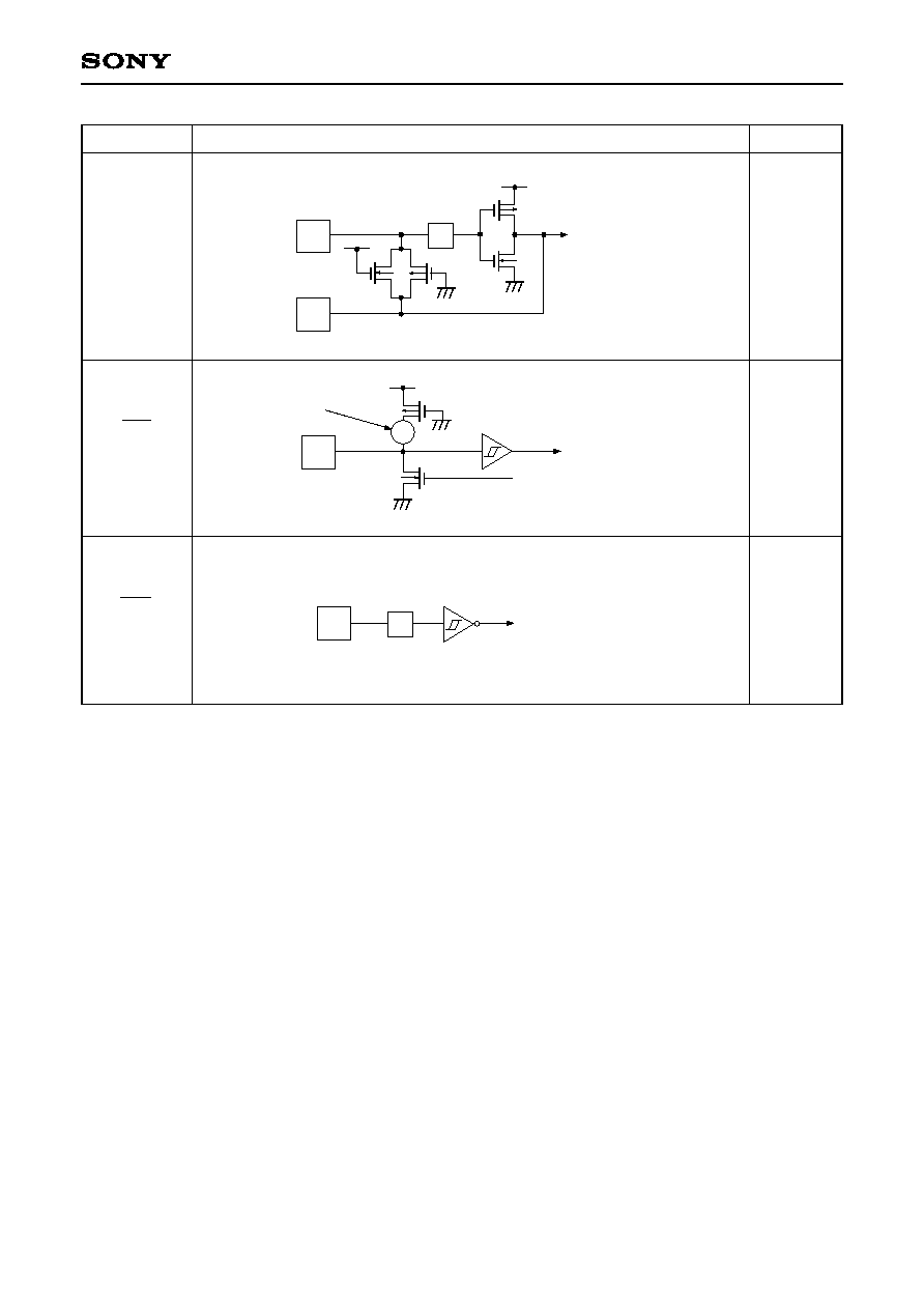
CXP875P40
Pin
Circuit format
When reset
Port H
Port H
Port H
Port H
Hi-Z
Hi-Z
Hi-Z
Open
PH0/SCK1
1 pin
PH1/SO1
1 pin
PH2/SI1
PH3/CS1/
INT1
2 pins
PH4
to
PH7
4 pins
SCK1 output enable
Internal serial clock from SI0
IP
Schmitt input
Data bus
RD (Port H)
External serial clock to SI0
SO1 output enable
SO1 from SI0
IP
Data bus
RD (Port H)
IP
Data bus
Schmitt input
RD (Port H)
Data bus
RD (Port H)
Port H data
Large current
12mA
Middle tension
proof 12V

≠ 10 ≠
CXP875P40
Port I
Port J
Port K
Hi-Z
Hi-Z
Hi-Z
When buffer
amplifier input is
selected, pulled
up interually
during standby.
PI0
to
PI7
8 pins
PJ0
to
PJ7
8 pins
PK0/RFDT
1 pin
Data bus
RD (Port I)
Port I direction
Port I data
IP
Input protection
circuit
(Every 4 bits)
Buffer
Data bus
RD (Port J)
Port J direction
Port J data
IP
(Every 4 bits)
Data bus
RD (Port K)
Port K direction
Port K data
IP
Input protection
circuit
(Every bit)
Servo input
Buffer amplifier input can be selected with the mask option.
Pin
Circuit format
When reset
≠ 11 ≠
CXP875P40
Pin
Circuit format
When reset
Port K
Port K
Hi-Z
Hi-Z
Hi-Z
Hi-Z
PK1/MCLK
1 pin
PK2
to
PK3
2 pins
CS0
SI0
2 pins
SO0
1 pin
Hi-Z
SCK0
1 pin
Data bus
RD (Port K)
Port K direction
Port K data
IP
Input protection
circuit
(Every bit)
Servo input
TTL schmitt input can be selected
with the mask option.
Data bus
RD (Port K)
Port K direction
Port K data
IP
(Every bit)
IP
Schmitt input
To SI0
SO0 output enable
SO0 from SI0
SCK0 output enable
Internal serial clock
from SI0
IP
Schmitt input
External serial clock to SI0
≠ 12 ≠
CXP875P40
EXTAL
XTAL
Oscillation
1 pin
2 pins
RST
1 pin
L level
NMI
Hi-Z
IP
EXTAL
XTAL
∑ Shows the circuit
composition during
oscillation.
∑ Feedback resistor is
removed during stop.
Schmitt input
Pull-up resistor
From power on reset circuit
(Mask option)
Mask option
OP
IP
Schmitt input
Interruption circuit
Pin
Circuit format
When reset

≠ 13 ≠
CXP875P40
Absolute Maximum Ratings
(V
SS
= 0V)
1
AV
DD
and V
DD
should be set to the same voltage.
2
V
IN
and V
OUT
should not exceed V
DD
+ 0.3V
3
The large current operation transistors are the N-ch transistors of the PD and PH4 to PH7.
Note) Usage exceeding absolute maximum ratings may permanently impair the LSI. Normal operation should
better take place under the recommended operating conditions. Exceeding those conditions may
adversely affect the reliability of the LSI.
Power supply voltage
Input voltage
Output voltage
Middle tension proof output voltage
High level output current
High level total output current
Low level total output current
Operating temperature
Storage temperature
Low level output current
Allowable power dissipation
V
DD
V
PP
AV
DD
AV
SS
V
IN
V
OUT
V
OUTP
I
OH
I
OH
I
OL
I
OLC
I
OL
Topr
Tstg
P
D
mW
≠0.3 to +7.0
≠0.3 to +13.0
AV
SS
to +7.0
1
≠0.3 to +0.3
≠0.3 to +7.0
2
≠0.3 to +7.0
2
≠0.3 to +15.0
≠5
≠50
15
20
130
≠10 to +75
≠55 to +150
600
380
V
V
V
V
V
V
mA
mA
mA
mA
mA
∞C
∞C
PROM version only
PH pin
Total of entire output pins
Other than large current output pins : per pin
Large current port pin
3
: per pin
Total of entire output pins
QFP package
LQFP package
Item
Symbol
Ratings
Unit
Remarks
≠ 14 ≠
CXP875P40
Recommended Operating Conditions
(V
SS
= 0V)
1
AV
DD
and V
DD
should be set to the same voltage.
2
Normal input port (Each pin of PC, PD, PF and PH1).
3
Each pin of NMI, CS0, SI0, SCK0, RST, PE0/INT0, PE1/EC/INT2, PH0/SCK1, PH2/SI1, PH3/INT1/CS1,
PG and PK1/MCLK (when CMOS schmitt input is selected with mask option for PG, PK1/MCLK).
4
Each pin of PG and PK1/MCLK (when TTL schmitt input is selected with mask option).
5
Specified only during external clock input.
6
V
PP
and V
DD
should be set to same voltage.
Analog power supply
High level input
voltage
Low level input
voltage
Operating temperature
5.5
5.5
5.5
V
DD
V
DD
V
DD
V
DD
+ 0.3
0.3V
DD
0.2V
DD
0.8
0.4
+75
V
V
V
V
V
V
V
V
V
V
∞C
V
Item
Symbol
Min.
Max.
Unit
Remarks
4.5
2.5
4.5
0.7V
DD
0.8V
DD
2.2
V
DD
≠ 0.4
0
0
0
≠0.3
≠10
V
PP
AV
DD
V
IH
V
IHS
V
IHTS
V
IHEX
V
IL
V
ILS
V
ILTS
V
ILEX
Topr
Guaranteed range during operation
Guaranteed data hold operation range during STOP
6
1
2
CMOS schmitt input
3
TTL schmitt input
4
EXTAL pin
5
2
CMOS schmitt input
3
TTL schmitt input
4
EXTAL pin
5
V
DD
Power supply voltage
V
PP
= V
DD

≠ 15 ≠
CXP875P40
DC Characteristics
(Ta = ≠10 to +75∞C, V
SS
= 0V)
1
RST pin specifies only when the power on reset circuit is selected with mask option.
2
RST pin specifies the input current when the pull-up resistance is selected, and specifies leakage current
when non-resistance is selected.
3
PK0 pin specifies only when the normal input circuit is selected with mask option.
V
DD
= 4.5V, I
OH
= ≠0.5mA
V
DD
= 4.5V, I
OH
= ≠1.2mA
V
DD
= 4.5V, I
OL
= 1.8mA
V
DD
= 4.5V, I
OL
= 3.6mA
V
DD
= 4.5V, I
OL
= 12.0mA
V
DD
= 5.5V, V
IH
= 5.5V
V
DD
= 5.5V, V
IL
= 0.4V
V
DD
= 5.5V, V
IL
= 0.4V
V
DD
= 5.5V
V
I
= 0, 5.5V
V
DD
= 5.5V
V
OH
= 12V
Operating mode
(1/2 dividing clock)
12.288MHz crystal
oscillation
(C
1
= C
2
= 12pF)
Entire output pins open
SLEEP mode
STOP mode
Clock 1MHz
0V other than the
measured pins
High level
output voltage
4.0
3.5
0.5
≠0.5
≠1.5
0.4
0.6
1.5
40
≠40
≠400
±10
50
V
V
V
V
V
µA
µA
µA
µA
µA
PD, PH4 to PH7
PA to PD, PE2 to PE7,
PH0, PH1, SO0, SCK0
PH4 to PH7
(V
OL
only)
RST
1
(V
OL
only)
PI to PK
EXTAL
RST
2
PA to PG
PH0 to PH3,
CS0, SI0, SO0,
SCK0, NMI,
RST
2
PI to PK
3
PH4 to PH7
Item
Symbol
Pin
Condition
Min.
Typ.
Max. Unit
Other than V
DD
,
V
SS
, AV
DD
, and
AV
SS
pins
V
DD
mA
mA
µA
pF
45
17
30
20
20
5
10
I
LOH
I
DD
I
DDSL
I
DDST
C
IN
V
OH
V
OL
I
IHE
I
ILE
I
ILR
I
IZ
Low level
output voltage
Input current
I/O leakage
current
Open drain output
leakage current
(N-ch Tr OFF in
state)
Current power
supply
Input capacity
≠ 16 ≠
CXP875P40
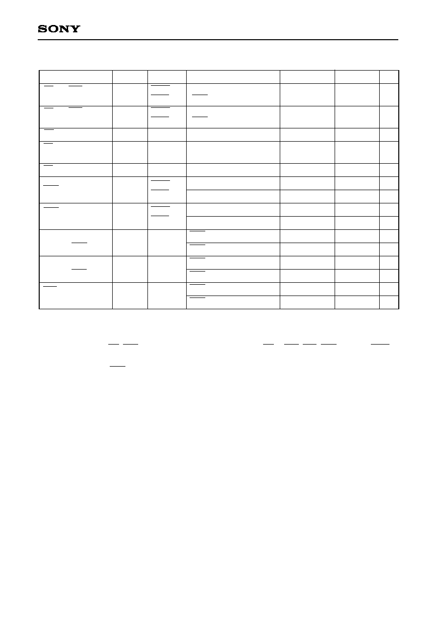
AC Characteristics
(1) Clock timing
(Ta = ≠10 to +75∞C, V
DD
= 4.5 to 5.5V, V
SS
= 0V)
t
sys indicates three values according to the contents of the clock control register (address : 00FE
H
) upper 2
bits (CPU clock selection).
t
sys (ns) = 2000/fc (Upper 2 bits = "00"), 4000/fc (Upper 2 bits = "01"), 16000/fc (Upper 2 bits = "11")
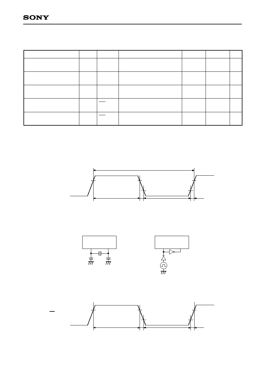
System clock frequency
System clock input pulse
width
System clock input rising
and falling times
Event count input clock
pulse width
Event count input clock
rising and falling times
f
C
t
XL
,
t
XH
t
CR
,
t
CF
t
EH
,
t
EL
t
ER
,
t
EF
XTAL
EXTAL
EXTAL
EXTAL
EC
EC
12.288
200
20
MHz
ns
ns
ns
ms
Item
Symbol
Pin
Condition
Min.
Max.
Unit
Fig. 1, Fig. 2
Fig. 1, Fig. 2
External clock drive
Fig. 1, Fig. 2
External clock drive
Fig. 3
Fig. 3
1
36
t
sys + 50
Crystal oscillation
Ceramic oscillation
EXTAL
XTAL
External clock
EXTAL
XTAL
C1
C2
Fig. 2. Clock applying condition
Fig. 1. Clock timing
EXTAL
t
XH
t
XL
t
CF
t
CR
0.4V
V
DD
≠ 0.4V
1/fc
Fig. 3. Event count clock timing
EC
t
EH
t
EL
t
EF
t
ER
0.2V
DD
0.8V
DD
74HCO4
≠ 17 ≠
CXP875P40
(2) Serial transfer
(Ta = ≠10 to +75∞C, V
DD
= 4.5 to 5.5V, V
SS
= 0V)
Note 1)
t
sys indicates three values according to the contents of the clock control register (address : 00FE
H
)
upper 2 bits (CPU clock selection).
t
sys (ns) = 2000/fc (Upper 2 bits = "00"), 4000/fc (Upper 2 bits = "01"), 16000/fc (Upper 2 bits = "11")
Note 2)
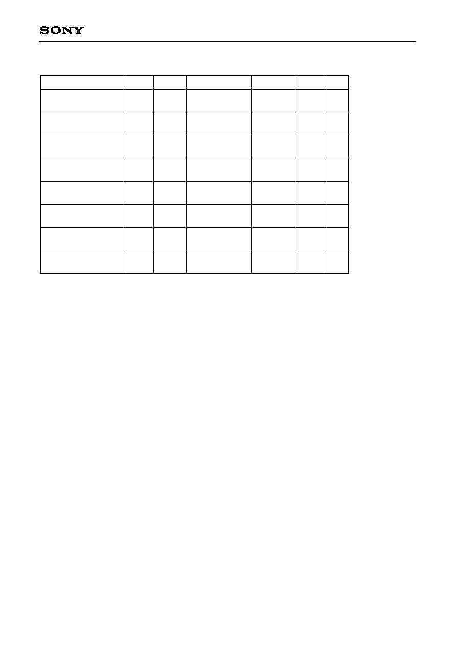
The marks CS, SCK, SI and SO respectivery mean pins of CS
CS0, CS1, SCK
SCK0, SCK1,
SI
SI0, SI1 and SO
SO0, SO1.
Note 3)
The load of SCK output mode and SO output delay time is 50pF + 1TTL.
CS
SCK delay
time
CS
SCK floating
delay time
CS
SO delay time
CS
SO floating
delay time
CS high level width
t
sys + 200
2
t
sys + 200
8000/fc
t
sys + 100
4000/fc ≠ 50
≠
t
sys + 100
200
2
t
sys + 100
100
t
sys + 200
t
sys + 200
t
sys + 200
t
sys + 200
2
t
sys + 200
100
ns
ns
ns
ns
ns
ns
ns
ns
ns
ns
ns
ns
ns
ns
ns
Item
Symbol
Pin
Condition
Min.
Max.
Unit
Chip select transfer mode
(SCK = Output mode)
Chip select transfer mode
(SCK = Output mode)
Chip select transfer mode
Chip select transfer mode
Chip select transfer mode
Input mode
Output mode
Input mode
Output mode
SCK input mode
SCK output mode
SCK input mode
SCK output mode
SCK input mode
SCK output mode
SCK cycle time
SCK high and low
level widths
SI input setup time
(against SCK
)
SI input hold time
(against SCK
)
SCK
SO delay
time
t
DCSK
t
DCSKF
t
DCSO
t
DCSOF
t
WHCS
t
KCY
t
KH
t
KL
t
SIK
t
KSI
t
KSO
SCK0,
SCK1
SCK0,
SCK1
SO0, SO1
SO0, SO1
CS0, CS1
SCK0,
SCK1
SCK0,
SCK1
SI0, SI1
SI0, SI1
SO0, SO1
≠ 18 ≠
CXP875P40
Fig. 4. Serial transfer timing
CS0
CS1
SCK0
SCK1
0.2V
DD
0.8V
DD
t
WHCS
t
DCSK
t
DCSKF
0.8V
DD
0.2V
DD
0.8V
DD
t
KCY
t
KL
t
KH
0.8V
DD
0.2V
DD
SI0
SI1
t
SIK
t
KSI
Input
data
t
DCSO
t
KSO
t
DCSOF
Output
data
0.8V
DD
0.2V
DD
SO0
SO1
≠ 19 ≠
CXP875P40
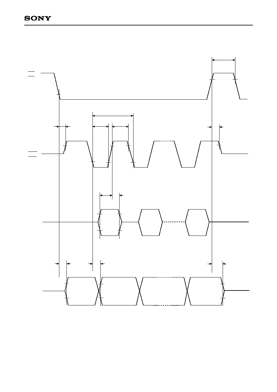
(3) A/D converter characteristics
(Ta = ≠10 to +75∞C, V
DD
= AV
DD
= 4.5 to 5.5V, AV
REF
= 4.0 to AV
DD
, V
SS
= AV
SS
= 0V)
Conversion time
Sampling time
Reference input
voltage
Analog input
voltage
V
ZT
1
V
FT
2
30
4970
t
CONV
t
SAMP
V
REF
V
IAN
I
REF
AV
REF
AN0 to
AN7
Ta = 25∞C
V
DD
= AV
DD
= 5.0V
V
SS
= AV
SS
= 0V
Operating mode
SLEEP mode
STOP mode
Linearity error
Zero transition
voltage
Resolution
AV
REF
current
AV
REF
I
REFS
µs
µs
V
V
AV
DD
AV
REF
1.0
mA
10
µA
0.6
160/f
C
12/f
C
AV
DD
≠ 0.5
0
Item
Symbol
Pin
Condition
Min.
Typ.
Max.
Unit
Full scale
transition voltage
≠10
4930
8
±1
70
5010
bits
LSB
mV
mV
Fig. 5. Definitions of A/D converter terms
Analog input
Linearity
error
V
FT
V
ZT
00
H
01
H
FE
H
FF
H
Digital conversion value
1
V
ZT
:Indicates the value that digital conversion value
changes from 00
H
to 01
H
and vice versa.
2
V
FT
:Indicates the value that digital conversion value
changes from FE
H
to FF
H
and vice versa.
≠ 20 ≠
CXP875P40
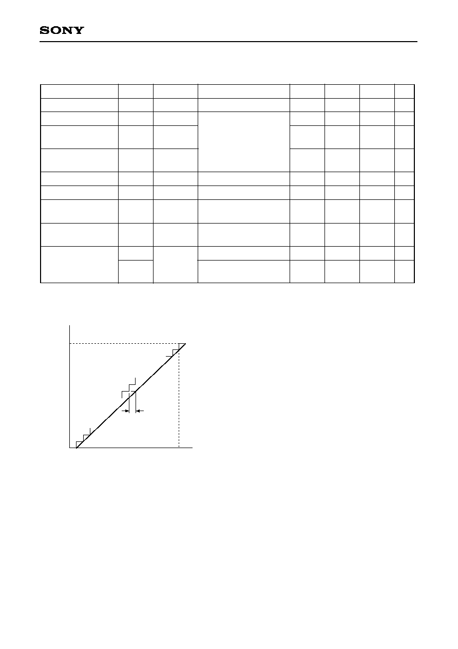
(4) Interruption, reset input
(Ta = ≠10 to +75∞C, V
DD
= 4.5 to 5.5V, V
SS
= 0V)
(5) Power on reset
Power on reset
(Ta = ≠10 to +75∞C, V
DD
= 4.5 to 5.5V, V
SS
= 0V)
External interruption high
and low level widths
Reset input low level width
INT0
INT1
INT2
NMI
RST
1
8/fc
µs
µs
Item
Symbol
Pin
Condition
Min.
Max.
Unit
t
IH
t
IL
t
RSL
Power supply rising
time
Power supply cut-off
time
t
R
t
OFF
V
DD
Power on reset
Repetitive power on reset
0.05
1
50
ms
ms
Item
Symbol
Pin
Condition
Min.
Max.
Unit
Fig. 6. Interruption input timing
Fig. 7. RST input timing
0.2V
DD
0.8V
DD
t
IH
t
IL
t
RSL
0.2V
DD
RST
INT0
INT1
INT2
NMI
(Falling edge)
Fig. 8. Power on reset
0.2V
0.2V
4.5V
V
DD
t
R
t
OFF
The power supply should rise smoothly.
Specifies only when power on reset function is selected.
≠ 21 ≠
CXP875P40
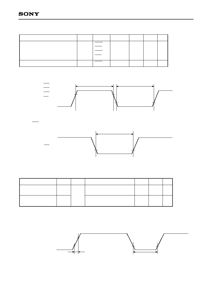
(6) Others
(Ta = ≠10 to +75∞C, V
DD
= 4.5 to 5.5V, V
SS
= 0V)
t
MCK
indicates three values according to the contents of the ATF control register (address : 01EE
H
) bits 5 and
4 (MCLK input control).
t
MCK
(ns) =
t
MCH
or
t
MCL
(bits 5 and 4 = "00"), 2
t
MCH
or 2
t
MCL
(bits 5 and 4 = "01"), 4
t
MCH
or 4
t
MCL
(bits 5 and 4
= "10").
RFDT input high and
low level widths
MCLK input high and
low level widths
DREF input high and
low level widths
DPG input high and
low level widths
DFG input high and
low level widths
CFG input high and
low level widths
RFG input high and
low level widths
EXI input high and
low level widths
t
RDH
t
RDL
t
MCH
t
MCL
t
DRH
t
DRL
t
DPH
t
DPL
t
DFH
t
DFL
t
CFH
t
CFL
t
RFH
t
RFL
t
EIH
t
EIL
RFDT
MCLK
DREF
DPG
DFG
CFG
RFG0
RFG1
EXI0
EXI1
2.5
t
MCK
326/fc
t
sys + 200
t
sys + 200
t
sys + 200
t
sys + 200
t
sys + 200
t
sys + 200
ns
ns
ns
ns
ns
ns
ns
ns
Item
Symbol
Pin
Condition
Min.
Max.
Unit
t
sys = 2000/fc
≠ 22 ≠
CXP875P40
Fig. 9. Other timing
RFDT
t
RDH
t
RDL
MCLK
t
MCH
t
MCL
DREF
t
DRH
t
DRL
DPG
t
DPH
t
DPL
DFG
t
DFH
t
DFL
CFG
t
CFH
t
CFL
RFG0
RFG1
t
RFH
t
RFL
EXI0
EXI1
t
EIH
t
EIL
≠ 23 ≠
CXP875P40
When buffer amplifier input circuit format of RFDT pin is selected with option.
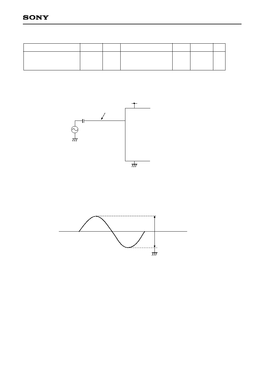
Note) V
APP
waveform indicates the range like Fig. 11. When composed by circuits other than Fig. 10. (when
DC bias does not become V
DD
/2), it should not exceed V
DD
+ 0.3 (V) and ≠0.3 (V) (V
SS
= 0V).
(7) Buffer amplifier function
(Ta = ≠10 to +75∞C, V
DD
= 4.5 to 5.5V, V
SS
= 0V)
Buffer amplifier input
voltage
(Peak to peak value)
V
APP
RFDT
When inputting 400kHz
sine wave on Fig. 10
circuit.
2.0
V
DD
+ 0.3
V
Item
Symbol
Pin
Condition
Min.
Max.
Unit
Fig. 10.
C
V
APP
(Refer to Fig. 11.)
C: 4700pF (±5%)
RFDT
V
DD
V
SS
Fig. 11.
V
APP
V
DD
/2
≠ 24 ≠
CXP875P40
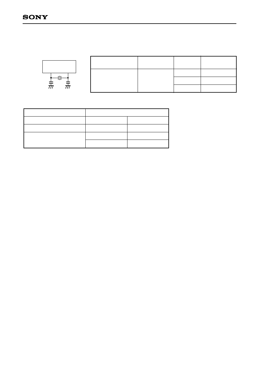
SUPPLEMENT
Mask option table
On PG0/EXI0 pin to PG7/RFG1 pin and PK1/MCLK pin, the input circuit format of CMOS schmitt or TTL
schmitt can be selected to every pin.
On PK0/RFDT pin, buffer amplifier or normal input circuit format can be selected.
EXTAL
XTAL
C1
C2
Fig. 12. SPC700 series recommended oscillation circuit
Model
Frequency
f (MHz)
C
1
, C
2
(pF)
RIVER ELETEC
CO., LTD.
HC-49/U-03
6.00
8.00
12.000
12
12
10
Manufacturer
Reset pin pull-up resistor
Power on reset circuit
Input circuit format
Non-existent
Non-existent
CMOS Schmitt
Buffer amplifier
Item
Contents
Existent
Existent
TTL Schmitt
Normal input
≠ 25 ≠
CXP875P40
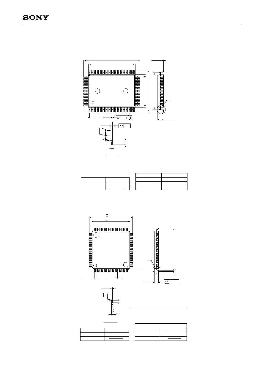
Package Outline
Unit: mm
SONY CODE
EIAJ CODE
JEDEC CODE
PACKAGE MATERIAL
LEAD TREATMENT
LEAD MATERIAL
PACKAGE WEIGHT
EPOXY RESIN
SOLDER PLATING
COPPER / 42 ALLOY
PACKAGE STRUCTURE
23.9 ± 0.4
QFP-100P-L01
DETAIL A
M
100PIN QFP (PLASTIC)
20.0 ≠ 0.1
+ 0.4
0∞ to 15∞
0.15 ≠ 0.05
+ 0.1
15.8 ±
0.4
17.9 ±
0.4
14.0 ≠ 0.01
+ 0.4
2.75 ≠ 0.15
+ 0.35
A
0.65
±0.12
0.15
0.8 ±
0.2
(16.3)
QFP100-P-1420-A
1.4g
SONY CODE
EIAJ CODE
JEDEC CODE
PACKAGE MATERIAL
LEAD TREATMENT
LEAD MATERIAL
PACKAGE WEIGHT
EPOXY/PHENOL RESIN
SOLDER PLATING
42 ALLOY
PACKAGE STRUCTURE
DETAIL A
LQFP-100P-L01
QFP100-P-1414-A
100PIN LQFP (PLASTIC)
16.0 ± 0.2
14.0 ± 0.1
75
51
50
26
25
1
76
0.5 ± 0.08
0.18 ≠ 0.03
+ 0.08
(0.22)
A
1.5 ≠ 0.1
+ 0.2
0.127 ≠ 0.02
+ 0.05
0.5 ±
0.2
(15.0)
0∞ to 10∞
0.1 ± 0.1
0.5 ±
0.2
100
0.1
NOTE: Dimension "
" does not include mold protrusion.