1
CXP912032
E95Y30B86-PS
CMOS 16-bit Single Chip Microcomputer
Description
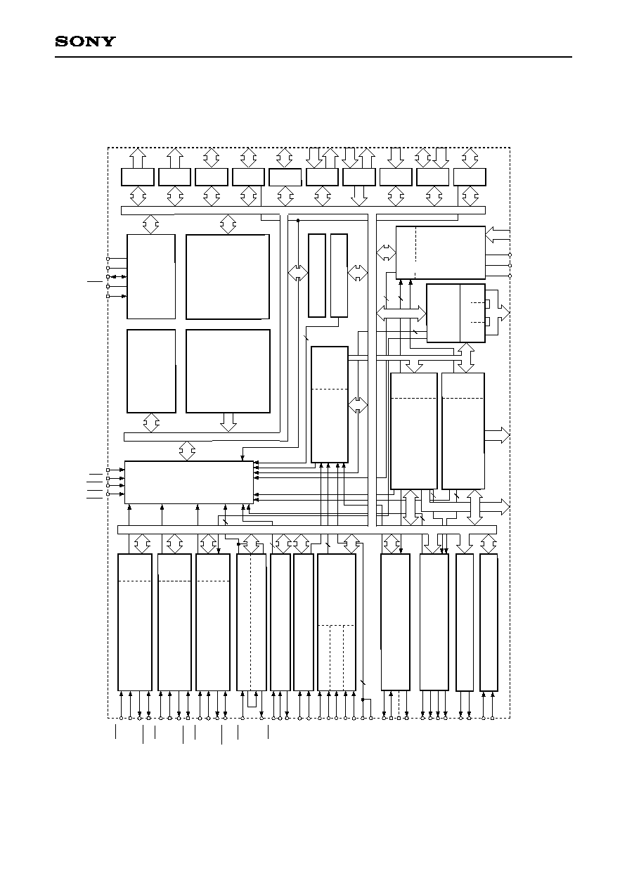
The CXP912032 is a CMOS 16-bit micro-computer
integrating on a single chip an A/D converter, serial
interface with an incorporated buffer RAM, high-
precision timing pattern generation function, pulse
cycle measurement circuit, PWM generator, general-
purpose prescaler, vertical sync separation circuit,
and a measurement circuit which measures the
signals of capstan FG, drum FG/PG, reel FG and
other servo systems with high precision, as well as
basic configurations like a 16-bit CPU, ROM, RAM,
and I/O port.
This LSI also provides sleep/stop modes that enable
lower power consumption.
Features
· An efficient instruction set as a controller
-- Direct addressing, numerous abbreviated forms,
multiplication and division instructions
· Instruction sets for C language and RTOS
-- Highly quadratic instruction system, general-purpose
register of 16-bit
×
8-pin
×
16-bank configuration
· Minimum instruction cycle time
100ns at 20MHz
operation
· Incorporated ROM capacity
128K bytes
· Incorporated RAM capacity
6144 bytes
· Peripheral functions
-- A/D converter
8-bit 12-channel successive approximation system, automatic
scanning function, 8-stage (soft) + 4-stage (hard) FIFO for
conversion results (Conversion time: 20µs at 20MHz)
-- Serial interface
Buffer RAM (128 bytes, supports high-speed transfer mode),
3 channels
-- Timers
8-bit timer/counter + 8-bit timer (with timing output), 1 channel
16-bit capture timer/counter (with timing output), 1 channel
16-bit timer, 4 channels
-- High-precision timing pattern generator PPG for 27 pins, 42 stages (max.)
PPG for 16 pins, 16 stages (max.)
RTG for 5 pins, 3 channels
-- PWM/DA gate output
PWM for 14 bits, 2 channels
(Repetitive frequency of 39.1kHz, 20MHz)
DA gate pulse for 14 bits, 2 channels
-- Servo input control
Capstan FG, drum FG/PG, reel FG
-- VSYNC separator
-- FRC capture unit
24-bit and 8-stage FIFO
-- PWM output
14 bits, 2 channels
-- General-purpose prescaler
10 bits, 1 channel
-- Pulse cycle measurement circuit
1 channel with mask input
· General-purpose I/O
80 pins
(max.; when all multi-purpose pins are used as general-purpose I/O.)
· Interruption
28 factors, 28 vectors, multi-interruption and priority selection
possible
· Standby mode
Sleep/stop
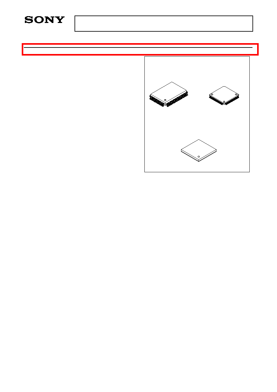
· Package
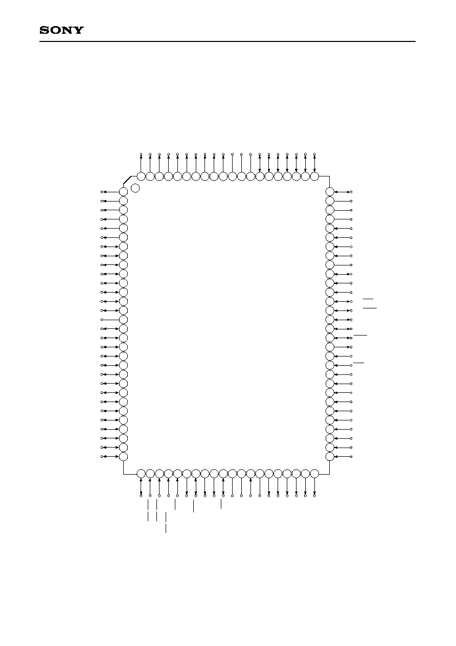
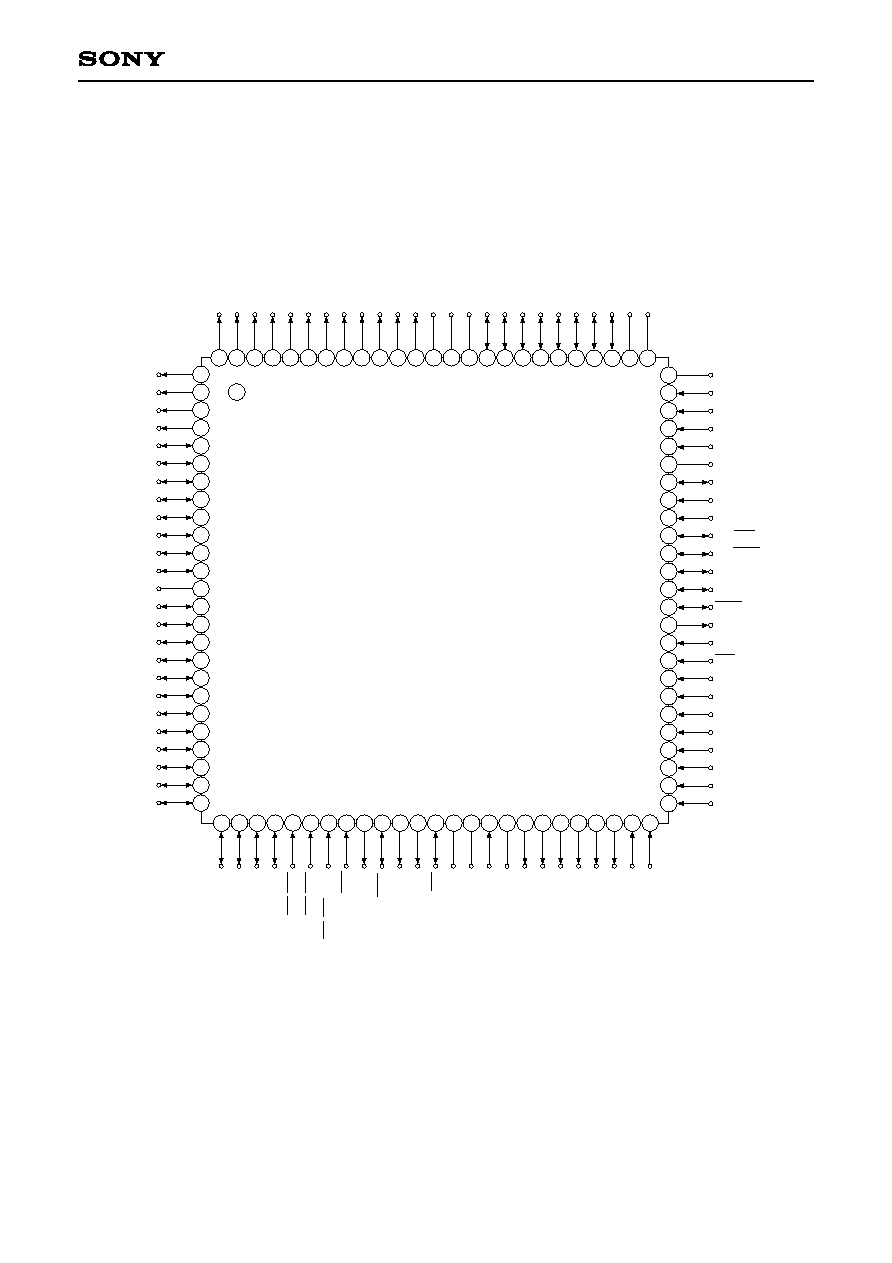
100-pin plastic QFP/LQFP, 104-pin plastic LFBGA
· Piggyback/evaluation chip
CXP912000 100-pin ceramic QFP/LQFP
Sony reserves the right to change products and specifications without prior notice. This information does not convey any license by
any implication or otherwise under any patents or other right. Application circuits shown, if any, are typical examples illustrating the
operation of the devices. Sony cannot assume responsibility for any problems arising out of the use of these circuits.
100 pin QFP (Plastic)
100 pin LQFP (Plastic)
104 pin LFBGA (Plastic)
Structure
Silicon gate CMOS IC
For the availability of this product, please contact the sales office.
5
CXP912032
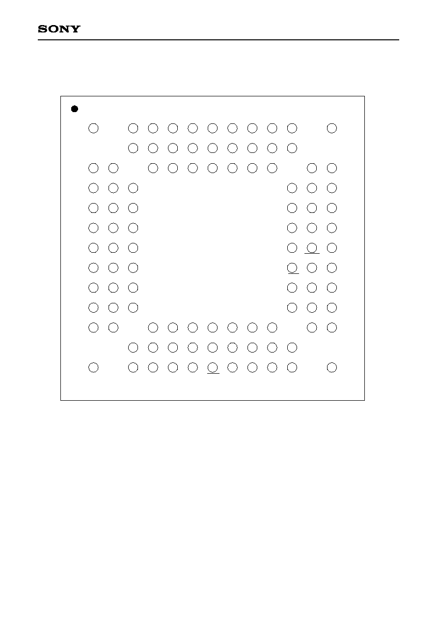
Pin Configuration 3 (Top View) 104-pin LFBGA Package
A11
A3
A13
A4
A5
A6
A7
A8
A9
A10
A1
B11
B3
B4
B5
B6
B7
B8
B9
B10
C2
C12
C13
C4
C5
C6
C7
C8
C9
C10
C1
D11
D2
D12
D3
D13
D1
E11
E2
E12
E3
E13
E1
F11
F2
F12
F3
F13
F1
G11
G2
G12
G3
G13
G1
H11
H2
H12
H3
H13
H1
J11
J2
J12
J3
J13
J1
K11
K2
K12
K3
K13
K1
L2
L12
L13
L4
L5
L6
L7
L8
L9
L10
L1
M11
M3
M4
M5
M6
M7
M8
M9
M10
N11
N3
N13
N4
N5
N6
N7
N8
N9
N10
N1
NC
1
2
3
4
5
6
7
8
9
10
11
12
13
A
B
C
D
E
F
G
H
J
K
L
M
N
PB1
PA7
PA4
PA1
V
SS
NC
PJ5
PJ2
PJ0
NC
PB2
PB0
PA5
PA2
V
DD
PJ7
PJ4
PJ1
AV
DD
PB6
PB5
PB3
PA6
PA3
PA0
PJ6
PJ3
AV
REF
AN2
PC0
PB4
AV
SS
PI7
PC3
PC1
V
SS
PI5
PC6
PC4
PI4
PI2
V
SS
PD0
PI1
PI0
PD1
PD3
CS0
SO0
PD4
PD6
PH5
PH7
PD7
PE3
PH0
PH4
PE1
PE4
PF1
PF4
V
SS
V
DD
PG2
PG7
PH2
PE5
PE7
PF2
PF5
PF7 EXTAL PG1
PG4
PG6
NC
PE6
PF0
PF3
PF6
RST
XTAL
PG0
PG3
PG5
NC
PE2
PE0
PD5
PD2
PC7
PC5
PC2
PB7
AN3
PH1
PH3
PH6
SI0
SCK0
PI3
PI6
AN1
Note) 1. Vss (Pins A7, E11, G1 and L7) must be connected to GND.
2. V
DD
(Pins B7 and L8) must be connected to V
DD
.
3. NC (Pins A1, A13, N1, N13 and A8) are left open.
4. A1, A13, N1 and N13 pins are reinforced balls.