CMOS 16-bit Single Chip Microcomputer
Description
The CXP921000A is a CMOS 16-bit single chip
microcomputer of piggyback/evaluator combined
type, which is developed for evaluating the function
of the CXP921064A.
Features
∑ An efficient instruction set as a controller
≠ Direct addressing, numerous abbreviated forms,
multiplication and division instructions
∑ Instruction sets for C Ianguage and RTOS
≠ Highly quadratic instruction system,
general-purpose register of eight 16-bit
◊
16-bank configuration
∑ Minimum instruction cycle time
100ns at 20MHz operation (2.7 to 3.3V)
61µs at 32kHz operation (2.2 to 3.3V)
∑ Incorporated EPROM
CXP27V1000K
∑ Incorporated RAM capacity
10K bytes
∑ Peripheral functions
-- A/D converter
8-bit 12 analog input, 2 channels successive approximation system,
automatic scanning function, (Conversion time: 3.4µs at 20MHz)
-- Serial interface
128 -byte buffer RAM, 3 channels
8-stage FIFO, 1 channel (supports special mode master/slave)
-- I
2
C bus interface
64-byte buffer RAM , 2 channels
(supports master/slave and automatic transfer mode)
-- Timers
8-bit timer/counter, 2 channels (with timing output)
16-bit timer, 3 channels
-- Real-time pulse generator
5-bit output, 1 channel (2-stage FIFO)
-- Clock prescaler
-- Remote control receive circuit
8-bit pulse measurement counter, 8-stage FIFO
∑ Interruption
30 factors, 30 vectors, multi-interruption and priority selection possible
∑ Standby mode
Sleep/stop
∑ Package
100-pin Ceramic PQFP
∑ Mask ROM
CXP921064A
∑ FLASH EEPROM incorporated type
CXP921F064A
Structure
Silicon gate CMOS IC
≠ 1 ≠
E99X11-PS
Sony reserves the right to change products and specifications without prior notice. This information does not convey any license by
any implication or otherwise under any patents or other right. Application circuits shown, if any, are typical examples illustrating the
operation of the devices. Sony cannot assume responsibility for any problems arising out of the use of these circuits.
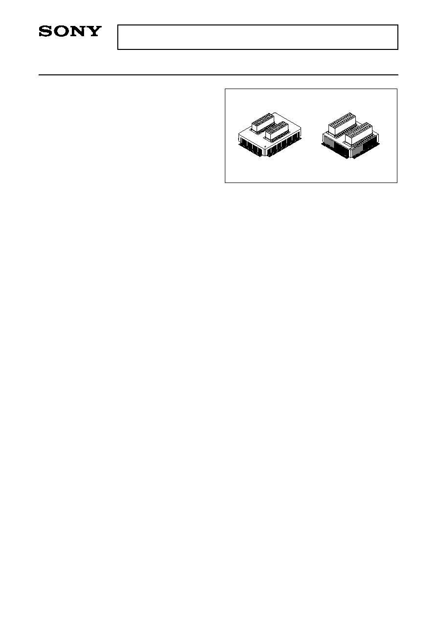
CXP921000A
100 pin PQFP (Ceramic)
Piggy/
evaluation type
(
QFP supported)
(LQFP supported)
≠ 2 ≠
CXP921000A
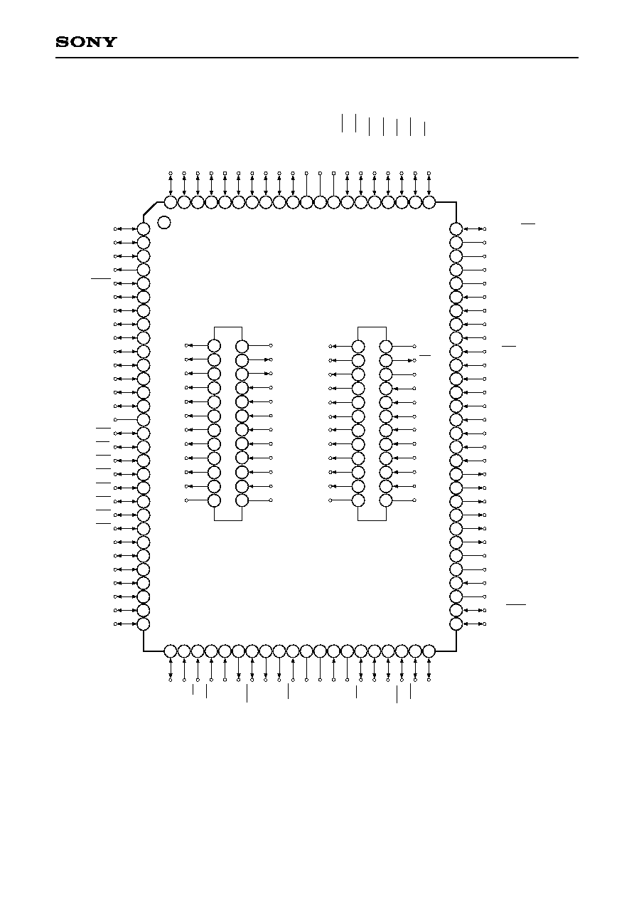
Pin Assignment in Piggyback Mode (Top View) 100-pin QFP package
31 32 33 34 35 36 37 38 39 40 41 42 43 44 45 46 47 48 49 50
57
58
59
60
61
62
63
64
65
66
67
68
69
70
71
72
73
74
75
76
77
78
79
80
81
82
83
84
85
86
87
88
89
90
91
92
93
94
95
96
97
98
99
1
2
3
4
5
6
7
8
9
10
11
12
13
14
15
16
17
18
19
20
21
22
23
24
P
E
7
P
F
0
P
F
1
/
E
C
P
F
2
/
C
S
0
P
F
3
/
S
I
0
P
F
4
/
S
O
0
P
F
5
/
S
C
K
0
P
F
6
/
T
O
P
F
7
/
T
M
O
R
S
T
V
S
S
X
T
A
L
E
X
T
A
L
V
D
D
P
G
0
/
C
S
1
P
G
1
/
S
I
1
P
G
2
/
S
O
1
P
G
3
/
S
C
K
1
P
G
4
/
C
S
2
P
G
5
/
S
I
2
PJ0/AN4/KS8
AV
DD
AV
REF1
AV
REF0
AVss
AN3
AN2
AN1
PI7/AN0
PI6/NMI
PI5/INT7
PI4/INT6
PI3/INT5
PI2/INT4
PI1/INT3
PI0/INT2
PH7/INT1
PH6/INT0
PH5/XOUT
PH4/RTO4
PH3/RTO3
PH2/RTO2
PH1/RTO1
PH0/RTO0
Vss
51
52
53
54
55
56
TX
TEX
V
DD
PG7/SCK2
PG6/SO2
PB2/AN22
PB3/AN23
PB4/SI3
PB5/SO3
PB6/SCK3
PB7/RMC
PC0/SDA0
PC1/SCL0
PC2/SDA1
PC3/SCL1
PC4
PC5
PC6
PC7
V
SS
PD0/KS0
PD1/KS1
PD2/KS2
PD3/KS3
PD4/KS4
PD5/KS5
PD6/KS6
PD7/KS7
PE0
25
26
27
28
29
PE1
PE2
PE3
PE4
PE5
30
PE6
P
B
1
/
A
N
2
1
P
B
0
/
A
N
2
0
P
A
7
/
A
N
1
9
P
A
6
/
A
N
1
8
P
A
5
/
A
N
1
7
P
A
4
/
A
N
1
6
P
A
3
/
A
N
1
5
P
A
2
/
A
N
1
4
P
A
1
/
A
N
1
3
P
A
0
/
A
N
1
2
V
S
S
V
D
D
N
C
P
J
7
/
A
N
1
1
/
K
S
1
5
P
J
6
/
A
N
1
0
/
K
S
1
4
P
J
5
/
A
N
9
/
K
S
1
3
P
J
4
/
A
N
8
/
K
S
1
2
P
J
3
/
A
N
7
/
K
S
1
1
P
J
2
/
A
N
6
/
K
S
1
0
P
J
1
/
A
N
5
/
K
S
9
100
1
2
3
4
5
6
7
8
9
10
11
12
13
14
15
16
17
18
19
20
21
22
23
24
A10
A9
A8
A7
A6
A5
A4
A3
A2
A1
A0
Vss
V
DD
A11
A12
D7
D6
D5
D4
D3
D2
D1
D0
Vss
25
26
27
28
29
30
31
32
33
34
35
36
37
38
39
40
41
42
43
44
45
46
47
48
A23
A22
A21
A20
A19
A18
A17
A16
A15
A14
A13
Vss
V
DD
CE
NC
D15
D14
D13
D12
D11
D10
D9
D8
Vss
Note) 1. NC (Pin 88) must be left open. However, use this pin for FLASH EEPROM
incorporated version.
2. Vss (Pins 15, 41, 56 and 90) must be connected to GND.
3. V
DD
(Pins 44, 53 and 89) must be connected to V
DD
.
4. A20 to A23 are always high level output.
≠ 3 ≠
CXP921000A
31 32 33 34 35 36 37 38 39 40 41 42 43 44 45 46 47 48 49 50
57
58
59
60
61
62
63
64
65
66
67
68
69
70
71
72
73
74
75
76
77
78
79
80
81
82
83
84
85
86
87
88
89
90
91
92
93
94
95
96
97
98
99
1
2
3
4
5
6
7
8
9
10
11
12
13
14
15
16
17
18
19
20
21
22
23
24
P
E
7
P
F
0
P
F
1
/
E
C
P
F
2
/
C
S
0
P
F
3
/
S
I
0
P
F
4
/
S
O
0
P
F
5
/
S
C
K
0
P
F
6
/
T
O
P
F
7
/
T
M
O
R
S
T
V
S
S
X
T
A
L
E
X
T
A
L
V
D
D
P
G
0
/
C
S
1
P
G
1
/
S
I
1
P
G
2
/
S
O
1
P
G
3
/
S
C
K
1
P
G
4
/
C
S
2
P
G
5
/
S
I
2
PJ0/AN4/KS8
AV
DD
AV
REF1
AV
REF0
AVss
AN3
AN2
AN1
PI7/AN0
PI6/NMI
PI5/INT7
PI4/INT6
PI3/INT5
PI2/INT4
PI1/INT3
PI0/INT2
PH7/INT1
PH6/INT0
PH5/XOUT
PH4/RTO4
PH3/RTO3
PH2/RTO2
PH1/RTO1
PH0/RTO0
Vss
51
52
53
54
55
56
TX
TEX
V
DD
PG7/SCK2
PG6/SO2
PB2/AN22
PB3/AN23
PB4/SI3
PB5/SO3
PB6/SCK3
PB7/RMC
PC0/SDA0
PC1/SCL0
PC2/SDA1
PC3/SCL1
PC4
PC5
PC6
PC7
V
SS
PD0/KS0
PD1/KS1
PD2/KS2
PD3/KS3
PD4/KS4
PD5/KS5
PD6/KS6
PD7/KS7
PE0
25
26
27
28
29
PE1
PE2
PE3
PE4
PE5
30
PE6
P
B
1
/
A
N
2
1
P
B
0
/
A
N
2
0
P
A
7
/
A
N
1
9
P
A
6
/
A
N
1
8
P
A
5
/
A
N
1
7
P
A
4
/
A
N
1
6
P
A
3
/
A
N
1
5
P
A
2
/
A
N
1
4
P
A
1
/
A
N
1
3
P
A
0
/
A
N
1
2
V
S
S
V
D
D
N
C
P
J
7
/
A
N
1
1
/
K
S
1
5
P
J
6
/
A
N
1
0
/
K
S
1
4
P
J
5
/
A
N
9
/
K
S
1
3
P
J
4
/
A
N
8
/
K
S
1
2
P
J
3
/
A
N
7
/
K
S
1
1
P
J
2
/
A
N
6
/
K
S
1
0
P
J
1
/
A
N
5
/
K
S
9
100
1
2
3
4
5
6
7
8
9
10
11
12
13
14
15
16
17
18
19
20
21
22
23
24
AD10
AD9
AD8
AD7
AD6
AD5
AD4
AD3
AD2
AD1
AD0
Vss
V
DD
AD11
AD12
I/T
MON
ERST
C1
C2
QS0
QS1
QS2
Vss
25
26
27
28
29
30
31
32
33
34
35
36
37
38
39
40
41
42
43
44
45
46
47
48
A23
A22
A21
A20
A19
A18
A17
A16
AD15
AD14
AD13
Vss
V
DD
E/P
ST0
ST1
ST2
ST3
WTACK
JRQH
JRQL
ENMI
MS
Vss
Pin Assignment in Evaluator Mode (Top View) 100-pin QFP package
Note) 1. NC (Pin 88) must be left open. However, use this pin for FLASH EEPROM
incorporated version.
2. Vss (Pins 15, 41, 56 and 90) must be connected to GND.
3. V
DD
(Pins 44, 53 and 89) must be connected to V
DD
.
≠ 4 ≠
CXP921000A
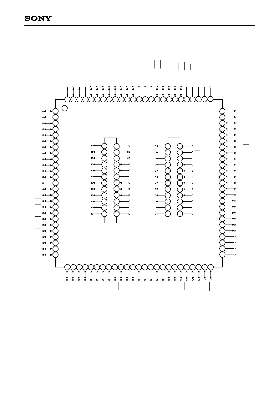
Pin Assignment in Piggyback Mode (Top View) 100-pin LQFP package
Note) 1. NC (Pin 86) must be left open. However, use this pin for FLASH EEPROM
incorporated version.
2. Vss (Pins 13, 39, 54 and 88) must be connected to GND.
3. V
DD
(Pins 42, 51 and 87) must be connected to V
DD
.
4. A20 to A23 are always high level output.
31 32 33 34 35 36 37 38 39 40 41 42 43 44 45 46 47 48 49 50
57
58
59
60
61
62
63
64
65
66
67
68
69
70
71
72
73
74
75
76
77
78
79
80
81
82
83
84
85
86
87
88
89
90
91
92
93
94
95
96
97
98
99
1
2
3
4
5
6
7
8
9
10
11
12
13
14
15
16
17
18
19
20
21
22
23
24
P
E
7
P
F
0
P
F
1
/
E
C
P
F
2
/
C
S
0
P
F
3
/
S
I
0
P
F
4
/
S
O
0
P
F
5
/
S
C
K
0
P
F
6
/
T
O
P
F
7
/
T
M
O
R
S
T
V
S
S
X
T
A
L
E
X
T
A
L
V
D
D
P
G
0
/
C
S
1
P
G
1
/
S
I
1
P
G
2
/
S
O
1
P
G
3
/
S
C
K
1
P
G
4
/
C
S
2
P
G
5
/
S
I
2
P
J
0
/
A
N
4
/
K
S
8
A
V
D
D
A
V
R
E
F
1
AV
REF0
AVss
AN3
AN2
AN1
PI7/AN0
PI6/NMI
PI5/INT7
PI4/INT6
PI3/INT5
PI2/INT4
PI1/INT3
PI0/INT2
PH7/INT1
PH6/INT0
PH5/XOUT
PH4/RTO4
PH3/RTO3
PH2/RTO2
PH1/RTO1
PH0/RTO0
Vss
51
52
53
54
55
56
TX
TEX
V
DD
PB4/SI3
PB5/SO3
PB6/SCK3
PB7/RMC
PC0/SDA0
PC1/SCL0
PC2/SDA1
PC3/SCL1
PC4
PC5
PC6
PC7
V
SS
PD0/KS0
PD1/KS1
PD2/KS2
PD3/KS3
PD4/KS4
PD5/KS5
PD6/KS6
PD7/KS7
PE0
25
26 27 28 29
PE1
PE2
PE3
30
P
E
4
P
E
5
P
E
6
P
B
1
/
A
N
2
1
P
B
2
/
A
N
2
2
P
B
3
/
A
N
2
3
P
B
0
/
A
N
2
0
P
A
7
/
A
N
1
9
P
A
6
/
A
N
1
8
P
A
5
/
A
N
1
7
P
A
4
/
A
N
1
6
P
A
3
/
A
N
1
5
P
A
2
/
A
N
1
4
P
A
1
/
A
N
1
3
P
A
0
/
A
N
1
2
V
S
S
V
D
D
N
C
P
J
7
/
A
N
1
1
/
K
S
1
5
P
J
6
/
A
N
1
0
/
K
S
1
4
P
J
5
/
A
N
9
/
K
S
1
3
P
J
4
/
A
N
8
/
K
S
1
2
P
J
3
/
A
N
7
/
K
S
1
1
P
J
2
/
A
N
6
/
K
S
1
0
P
J
1
/
A
N
5
/
K
S
9
100
P
G
7
/
S
C
K
2
P
G
6
/
S
O
2
1
2
3
4
5
6
7
8
9
10
11
12
13
14
15
16
17
18
19
20
21
22
23
24
A10
A9
A8
A7
A6
A5
A4
A3
A2
A1
A0
Vss
V
DD
A11
A12
D7
D6
D5
D4
D3
D2
D1
D0
Vss
25
26
27
28
29
30
31
32
33
34
35
36
37
38
39
40
41
42
43
44
45
46
47
48
A23
A22
A21
A20
A19
A18
A17
A16
A15
A14
A13
Vss
V
DD
CE
NC
D15
D14
D13
D12
D11
D10
D9
D8
Vss
≠ 5 ≠
CXP921000A
Pin Assignment in Evaluator Mode (Top View) 100-pin LQFP package
Note) 1. NC (Pin 86) must be left open. However, use this pin for FLASH EEPROM
incorporated version.
2. Vss (Pins 13, 39, 54 and 88) must be connected to GND.
3. V
DD
(Pins 42, 51 and 87) must be connected to V
DD
.
31 32 33 34 35 36 37 38 39 40 41 42 43 44 45 46 47 48 49 50
57
58
59
60
61
62
63
64
65
66
67
68
69
70
71
72
73
74
75
76
77
78
79
80
81
82
83
84
85
86
87
88
89
90
91
92
93
94
95
96
97
98
99
1
2
3
4
5
6
7
8
9
10
11
12
13
14
15
16
17
18
19
20
21
22
23
24
P
E
7
P
F
0
P
F
1
/
E
C
P
F
2
/
C
S
0
P
F
3
/
S
I
0
P
F
4
/
S
O
0
P
F
5
/
S
C
K
0
P
F
6
/
T
O
P
F
7
/
T
M
O
R
S
T
V
S
S
X
T
A
L
E
X
T
A
L
V
D
D
P
G
0
/
C
S
1
P
G
1
/
S
I
1
P
G
2
/
S
O
1
P
G
3
/
S
C
K
1
P
G
4
/
C
S
2
P
G
5
/
S
I
2
P
J
0
/
A
N
4
/
K
S
8
A
V
D
D
A
V
R
E
F
1
AV
REF0
AVss
AN3
AN2
AN1
PI7/AN0
PI6/NMI
PI5/INT7
PI4/INT6
PI3/INT5
PI2/INT4
PI1/INT3
PI0/INT2
PH7/INT1
PH6/INT0
PH5/XOUT
PH4/RTO4
PH3/RTO3
PH2/RTO2
PH1/RTO1
PH0/RTO0
Vss
51
52
53
54
55
56
TX
TEX
V
DD
PB4/SI3
PB5/SO3
PB6/SCK3
PB7/RMC
PC0/SDA0
PC1/SCL0
PC2/SDA1
PC3/SCL1
PC4
PC5
PC6
PC7
V
SS
PD0/KS0
PD1/KS1
PD2/KS2
PD3/KS3
PD4/KS4
PD5/KS5
PD6/KS6
PD7/KS7
PE0
25
26 27 28 29
PE1
PE2
PE3
30
P
E
4
P
E
5
P
E
6
P
B
1
/
A
N
2
1
P
B
2
/
A
N
2
2
P
B
3
/
A
N
2
3
P
B
0
/
A
N
2
0
P
A
7
/
A
N
1
9
P
A
6
/
A
N
1
8
P
A
5
/
A
N
1
7
P
A
4
/
A
N
1
6
P
A
3
/
A
N
1
5
P
A
2
/
A
N
1
4
P
A
1
/
A
N
1
3
P
A
0
/
A
N
1
2
V
S
S
V
D
D
N
C
(
P
W
E
)
P
J
7
/
A
N
1
1
/
K
S
1
5
P
J
6
/
A
N
1
0
/
K
S
1
4
P
J
5
/
A
N
9
/
K
S
1
3
P
J
4
/
A
N
8
/
K
S
1
2
P
J
3
/
A
N
7
/
K
S
1
1
P
J
2
/
A
N
6
/
K
S
1
0
P
J
1
/
A
N
5
/
K
S
9
100
P
G
7
/
S
C
K
2
P
G
6
/
S
O
2
1
2
3
4
5
6
7
8
9
10
11
12
13
14
15
16
17
18
19
20
21
22
23
24
AD10
AD9
AD8
AD7
AD6
AD5
AD4
AD3
AD2
AD1
AD0
Vss
V
DD
AD11
AD12
I/T
MON
ERST
C1
C2
QS0
QS1
QS2
Vss
25
26
27
28
29
30
31
32
33
34
35
36
37
38
39
40
41
42
43
44
45
46
47
48
A23
A22
A21
A20
A19
A18
A17
A16
AD15
AD14
AD13
Vss
V
DD
E/P
ST0
ST1
ST2
ST3
WTACK
JRQH
JRQL
ENMI
MS
Vss
≠ 6 ≠
CXP921000A
A0 to A23
D0 to D15
Address data
Input data
t
ACC
t
IH
0.8V
DD
0.2V
DD
0.8V
DD
0.2V
DD
EPROM Read Timing
(Ta = ≠20 to +75∞C, V
DD
= 2.7 to 3.3V, Vss = 0V)
Item
Address
data
Input delay time
Address
data
hold time
Symbol
t
ACC
t
IH
Pins
A0 to A23
D0 to D15
A0 to A23
D0 to D15
Min.
0
Max.
50
Unit
ns
ns
Product List
Optional item
Products
Piggy/evaluation chip
EPROM 256K bytes
Existent
Package
ROM capacity
Reset pin pull-up resistor
Mask ROM
CXP921064A
100-pin plastic QFP/LQFP
104-pin plastic LFLGA
256K bytes
Existent/Non-existent
CXP921000A-U01Q
100-pin ceramic PQFP
(QFP supported)
CXP921000A-U01R
100-pin ceramic PQFP
(LQFPsupported)
≠ 7 ≠
CXP921000A
Switching of Piggyback Mode and Evaluator Mode
Piggyback mode can be used by setting two LCC-type EPROM (for upper bytes, for lower byte) and connecting
to the connector of top of the chip.
Evaluator mode can be used by connecting in-circuit emulator CPU probe to the connector of top of the chip.
Piggyback mode
Evaluator mode
Pin 1 marking
0
1
LCC-type PROM
EPROM adaptor
Chip
For lower bytes
For upper bytes
Chip
CPU probe
Notes on PF7 Usage
FLASH EEPROM incorporated PF7 is also used as flash mode setting function. Note the followings:
1. "H" is output to PF7 during a reset. That is driven at comparatively high impedance (approximately 150k
),
and take care that V
OH
should not fall under 0.7V
DD
by the partial pressure with external circuit load
impedance.
2. When using software reset functions, PF7 may not rise enough during a reset. Switching PF7 to "H" output
prior to software reset execution or connecting pull-up resistor is recommended.
Mask ROM and piggy/evaluation chip do not have flash mode setting function. Considering that EEPROM
incorporated type is used, above countermeasure should be performed.
Keep PF7 above 0.7 V
DD
during
this period.
RST
PF7
Flash mode
Normal operation
≠ 8 ≠
CXP921000A
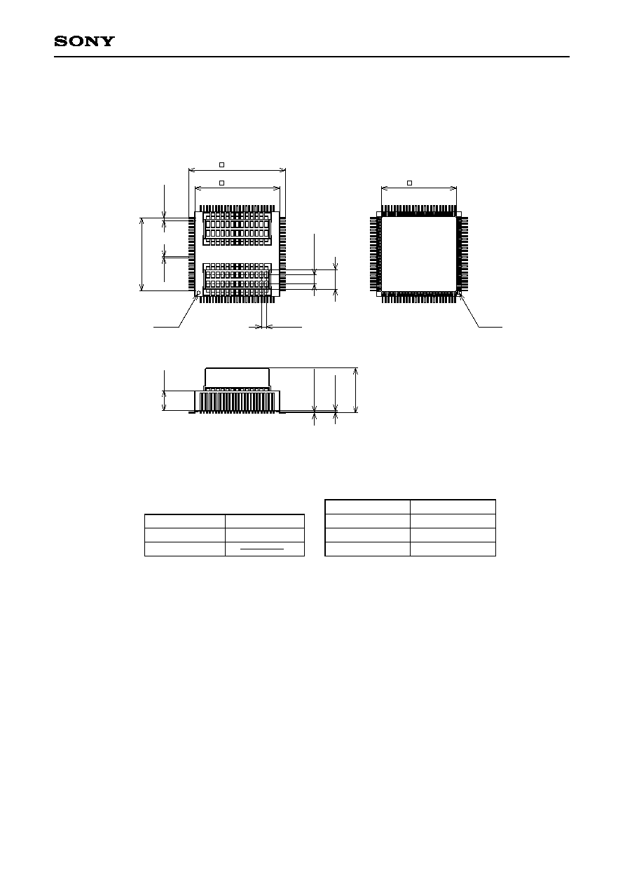
Package Outline
Unit: mm
SONY CODE
EIAJ CODE
JEDEC CODE
PACKAGE MATERIAL
LEAD TREATMENT
LEAD MATERIAL
PACKAGE MASS
CERAMIC
GOLD PLATING
42 ALLOY
PACKAGE STRUCTURE
1
30
31
50
51
80
81
100
1
6
.
3
±
0
.
2
1
8
.
7
±
0
.
5
22.3 ± 0.25
24.7 ± 0.5
0.8 ± 0.1
1
.
5
±
0
.
0
5
3
.
2
±
0
.
2
0
.
3
±
0
.
0
8
0
.
6
5
±
0
.
0
5
18.0
1
3
.
9
3
.
5
7
±
0
.
3
6
8
.
6
M
A
X
0
.
1
5
≠
0
.
0
2
+
0
.
0
5
0
.
5
±
0
.
2
5
100PIN PQFP(CERAMIC)
PQFP-100C-L04
4.9g
INDEX
INDEX
AQFP100-C-0000
≠ 9 ≠
CXP921000A
SONY CODE
EIAJ CODE
JEDEC CODE
PACKAGE MATERIAL
LEAD TREATMENT
LEAD MATERIAL
PACKAGE MASS
CERAMIC
GOLD PLATING
42 ALLOY
PACKAGE STRUCTURE
16.0 ± 0.5
14.0 ± 0.2
1
25
26
50
51
75
76
100
1
2
.
0
±
0
.
1
5
0
.
1
8
≠
0
.
0
3
+
0
.
0
8
0
.
5
±
0
.
0
5
1
.
5
±
0
.
0
5
3
.
2
±
0
.
2
0.8 ± 0.1
INDEX
12.4
INDEX
3
.
3
2
±
0
.
3
3
0
.
1
2
7
≠
0
.
0
2
0
.
2
≠
0
.
1
3
8
.
0
M
A
X
+
0
.
0
5
+
0
.
1
5
100PIN PQFP(CERAMIC)
PQFP-100C-L03
2.7g
AQFP100-C-0000