CMOS 16-bit Single Chip Microcomputer
Description
The CXP922000 is a CMOS 16-bit single chip
microcomputer of piggyback/evaluator combined
type, which is developed for evaluating the function
of the CXP922032.
Features
· An efficient instruction set as a controller
Direct addressing, numerous abbreviated forms,
multiplication and division instructions
· Instruction sets for C Ianguage and RTOS
Highly quadratic instruction system,
general-purpose register of eight 16-bit
×
16-bank configuration
· Minimum instruction cycle time
100ns at 20MHz operation (3.0 to 5.5V)
167ns at 12MHz operation (2.7 to 5.5V)
· Incorporated EPROM
CXP27V1000K
· Incorporated RAM capacity
7680 bytes
· Peripheral functions
A/D converter
8-bit 8 analog input, successive approximation system
(Conversion time: 12.4µs at 20MHz)
Serial interface
Asynchronous serial interface (Simple UART)
128-byte buffer RAM, 3 channels
Timers
8-bit timer/counter, 2 channels (with timing output)
16-bit capture timer/counter (with timing output)
16-bit timer, 4 channels
Remote control receive circuit
8-bit pulse measurement counter, 8-stage FIFO
PWM output circuit
14-bit, 1 channel
· Interruption
24 factors, 24 vectors, multi-interruption and priority selection possible
· Standby mode
Sleep/stop
· Package
100-pin ceramic PQFP
· Mask ROM
CXP922032
· One time PROM incorporated type
CXP922P032
Structure
Silicon gate CMOS IC
1
E98Z32B9X-PS
Sony reserves the right to change products and specifications without prior notice. This information does not convey any license by
any implication or otherwise under any patents or other right. Application circuits shown, if any, are typical examples illustrating the
operation of the devices. Sony cannot assume responsibility for any problems arising out of the use of these circuits.
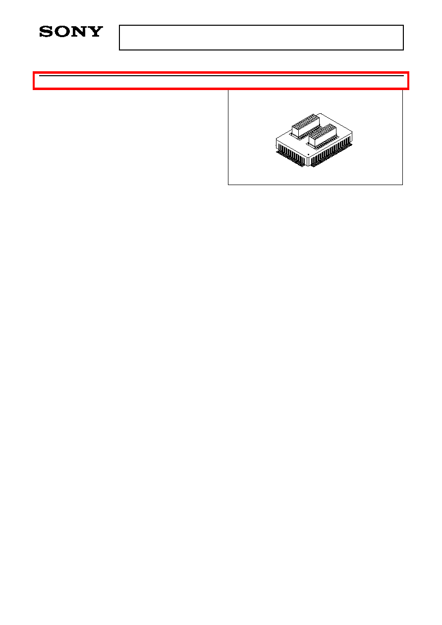
CXP922000
100 pin PQFP (Ceramic)
Piggy/
evaluation type
( QFP supported )
For the availability of this product, please contact the sales office.
2
CXP922000
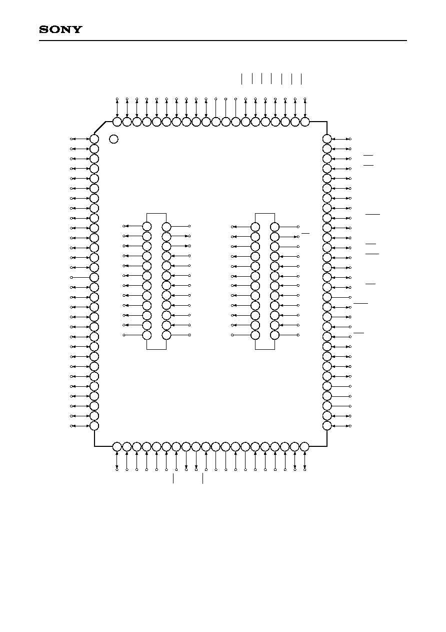
Pin Assignment in Piggyback Mode
1
2
3
4
5
6
7
8
9
10
11
12
13
14
15
16
17
18
19
20
21
22
23
24
25
26
27
28
29
30
31 32 33 34 35 36 37 38 39 40 41 42 43 44 45 46 47 48 49 50
51
52
53
54
55
56
57
58
59
60
61
62
63
64
65
66
67
68
69
70
71
72
73
74
75
76
77
78
79
80
81
82
83
84
85
86
87
88
89
90
91
92
93
94
95
96
97
98
99
100
1
2
3
4
5
6
7
8
9
10
11
12
13
14
15
16
17
18
19
20
21
22
23
24
25
26
27
28
29
30
31
32
33
34
35
36
37
38
39
40
41
42
43
44
45
46
47
48
P
B
1
P
B
0
P
A
7
P
A
6
P
A
5
P
A
4
P
A
3
P
A
2
P
A
1
P
A
0
V
s
s
V
D
D
N
C
P
J
6
/
K
S
6
P
J
5
/
K
S
5
P
J
4
/
K
S
4
P
J
3
/
K
S
3
P
J
2
/
K
S
2
P
J
1
/
K
S
1
P
J
0
/
K
S
0
P
E
7
P
F
0
/
I
N
T
0
P
F
1
/
I
N
T
1
P
F
2
/
I
N
T
2
P
F
3
/
I
N
T
3
P
F
4
/
I
N
T
4
P
F
5
/
N
M
I
P
F
6
/
T
O
0
P
F
7
/
T
O
1
/
P
W
M
R
S
T
V
s
s
X
T
A
L
E
X
T
A
L
V
D
D
A
N
0
A
N
1
A
N
2
A
N
3
P
G
0
/
A
N
4
P
G
1
/
A
N
5
PB2
PB3
PB4
PB5
PB6
PB7
PC0
PC1
PC2
PC3
PC4
PC5
PC6
PC7
Vss
PD0
PD1
PD2
PD3
PD4
PD5
PD6
PD7
PE0
PE1
PE2
PE3
PE4
PE5
PE6
PI7/RMC
PI6/CINT
PI5/EC1
PI4/EC0
PI3
PI2
PI1/RxD
PI0/TxD
PH7/SCK2
PH6/SO2
PH5/SI2
PH4/CS2
PH3/SCK1
PH2/SO1
PH1/SI1
PH0/CS1
Vss
SCK0
SO0
SI0
CS0
PG7
PG6
PG5
PG4
AV
DD
AV
REF
AV
SS
PG3/AN7
PG2/AN6
A10
A9
A8
A7
A6
A5
A4
A3
A2
A1
A0
Vss
A23
A22
A21
A20
A19
A18
A17
A16
A15
A14
A13
Vss
V
DD
A11
A12
D7
D6
D5
D4
D3
D2
D1
D0
Vss
V
DD
CE
NC
D15
D14
D13
D12
D11
D10
D9
D8
Vss
Note) 1. Do not make any connections to NC (Pin 88 ).
2. Vss (Pins 15, 41, 64 and 90) are connected to GND.
3. V
DD
(Pins 44 and 89) are both connected to V
DD
.
4. A19 to A23 are always high level output.

3
CXP922000
1
2
3
4
5
6
7
8
9
10
11
12
13
14
15
16
17
18
19
20
21
22
23
24
25
26
27
28
29
30
31 32 33 34 35 36 37 38 39 40 41 42 43 44 45 46 47 48 49 50
51
52
53
54
55
56
57
58
59
60
61
62
63
64
65
66
67
68
69
70
71
72
73
74
75
76
77
78
79
80
81
82
83
84
85
86
87
88
89
90
91
92
93
94
95
96
97
98
99
100
1
2
3
4
5
6
7
8
9
10
11
12
13
14
15
16
17
18
19
20
21
22
23
24
25
26
27
28
29
30
31
32
33
34
35
36
37
38
39
40
41
42
43
44
45
46
47
48
P
B
1
P
B
0
P
A
7
P
A
6
P
A
5
P
A
4
P
A
3
P
A
2
P
A
1
P
A
0
V
s
s
V
D
D
N
C
P
J
6
/
K
S
6
P
J
5
/
K
S
5
P
J
4
/
K
S
4
P
J
3
/
K
S
3
P
J
2
/
K
S
2
P
J
1
/
K
S
1
P
J
0
/
K
S
0
P
E
7
P
F
0
/
I
N
T
0
P
F
1
/
I
N
T
1
P
F
2
/
I
N
T
2
P
F
3
/
I
N
T
3
P
F
4
/
I
N
T
4
P
F
5
/
N
M
I
P
F
6
/
T
O
0
P
F
7
/
T
O
1
/
P
W
M
R
S
T
V
s
s
X
T
A
L
E
X
T
A
L
V
D
D
A
N
0
A
N
1
A
N
2
A
N
3
P
G
0
/
A
N
4
P
G
1
/
A
N
5
PB2
PB3
PB4
PB5
PB6
PB7
PC0
PC1
PC2
PC3
PC4
PC5
PC6
PC7
Vss
PD0
PD1
PD2
PD3
PD4
PD5
PD6
PD7
PE0
PE1
PE2
PE3
PE4
PE5
PE6
PI7/RMC
PI6/CINT
PI5/EC1
PI4/EC0
PI3
PI2
PI1/RxD
PI0/TxD
PH7/SCK2
PH6/SO2
PH5/SI2
PH4/CS2
PH3/SCK1
PH2/SO1
PH1/SI1
PH0/CS1
Vss
SCK0
SO0
SI0
CS0
PG7
PG6
PG5
PG4
AV
DD
AV
REF
AV
SS
PG3/AN7
PG2/AN6
AD10
AD9
AD8
AD7
AD6
AD5
AD4
AD3
AD2
AD1
AD0
Vss
A23
A22
A21
A20
A19
A18
A17
A16
AD15
AD14
AD13
Vss
V
DD
AD11
AD12
I/T
MON
ERST
C1
C2
QS0
QS1
QS2
Vss
V
DD
E/P
ST0
ST1
ST2
ST3
WTACK
JRQH
JRQL
ENMI
MS
Vss
Note) 1. Do not make any connections to NC (Pin 88 ).
2. Vss (Pins 15, 41, 64 and 90) are connected to GND.
3. V
DD
(Pins 44 and 89) are both connected to V
DD
.
Pin Assignment in Evaluator Mode

5
CXP922000
Switching of Piggyback Mode and Evaluator Mode
Piggyback mode can be used by setting two LCC-type EPROM (for upper bytes, for lower byte) and connecting
to the connector of top of the chip.
Evaluator mode can be used by connecting in-circuit emulator CPU probe to the connector of top of the chip.
Piggyback mode
Evaluator mode
Pin 1 marking
0
1
LCC-type PROM
EPROM adaptor
Chip
For lower bytes
For upper bytes
Chip
CPU probe